NJW4702
- 1 -
Ver.1
3ch Laser Diode Driver
s
s
s
s
GENERAL DESCRIPTION
s
s
s
s
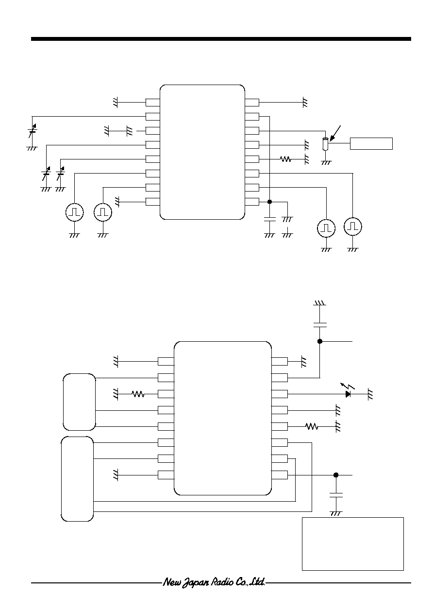
PACKAGE OUTLINE
NJW4702 is a laser diode driver for the operation of a grounded
laser diode for CD-R and CD-RW drivers.
It includes three channels current amplifiers for three different
optical power levels. Reference inputs are voltage input, and
voltage control is possible without external resistors. An on-chip RF
oscillator is provided to reduce laser mode noise during read mode.
Oscillation frequency and oscillation amplitude are defined by two
external resistors.
s
s
s
s
FEATURES
q
Operating Voltage 4.5V to 5.5V
q
On-chip RF Oscillator 200MHz to 500MHz
q
Rise-time/Fall-time 1.0ns typ.
q
Maximum Output Current 250mA typ.
q
Bi-CMOS Technology
q
Package Outline PCSP16(3.5mm 0.65mm pitch)
s
s
s
s
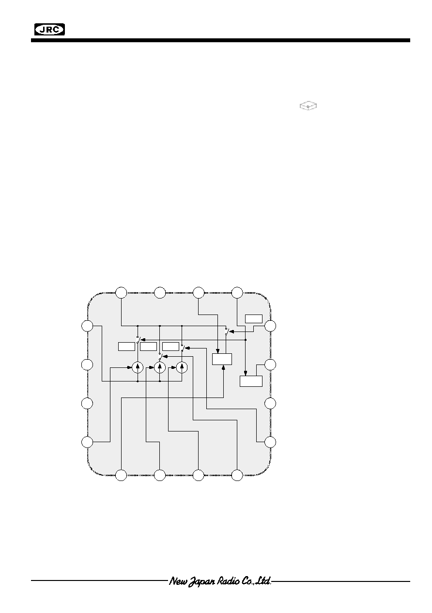
BLOCK DIAGRAM
VINR
VIN2
VIN3
IOUT
RAMP
RFREQ
VCC1
VCC2
GND
ENABLE
OUTEN2
OUTEN3
OSCEN
14
15
OSC
H:ON
L:ON
L:ON
H:ON
16
2
3
4
5
6
7
8
11
12
13
GND
GND
GND
1
10
9
BIAS
NJW4702SE8
Ver.1
NJW4702
- 2 -
s
s
s
s
ABSOLUTE MAXUIMUM RATING (Ta=25
�
C)
PARAMETERS SYMBOL
RATINGS
UNIT
Supply Voltage
V
+
6.0 V
Power Dissipation
P
D
860
*
mW
Operating Temperature Range
Topr
-40 to +85
�
C
Storage Temperature Range
Tstg
-40 to +125
�
C
*EIA/JEDEC STANDARD Test Board(76.2x114.3x1.6mm,4layers,FR-4)mounting
s
s
s
s
RECOMMENDED OPERATING CONDITION (Ta=25
�
C)
PARAMETERS SYMBOL
TEST
CONDITION
MIN.
TYP.
MAX.
UNIT
Operating
Voltage
Vopr
4.5 5.0 5.5 V
s
s
s
s
ELECTRICAL CHARACTERISTICS
q
DC CHARACTERISTICS
(Vcc=5.0V,ENABLE=H,OUTEN=H,OSCEN=L, H:5V,L:GND,2V to Iout, Ta=25
�
C unless otherwise specified)
PARAMETERS SYMBOL
TEST
CONDITION
MIN.
TYP.
MAX.
UNIT
Supply Current 1
I
CC
1
ENABLE
0.5V
- 0 10
�
A
Supply Current 2
I
CC
2 VINR/2/3=0V
-
5
7 mA
Supply Current 3
I
CC
3
OSCEN=H,RAMP=1k
,RFREQ=3.6k
- 55 75
mA
Supply Current 4
I
CC
4 VINR=0V,VIN2=0.3V,VIN3=0.3V
-
20 30 mA
Supply Current 5
I
CC
5 VINR=0.8V,VIN2/3=0.3V
-
80 110 mA
High Level Input Voltage
VIH
3.5
-
-
V
Low level Input Voltage
VIL
-
-
1.5
V
High Level Input Current
IIH
-
- 100
�
A
Low Level Input Current
IIL
-100
-
-
�
A
Shutdown Voltage
Vshut
VINR=0.8V,VIN2/3=0.3V,
OUTEN=L,OSCEN=H,Vcc at Icc
1mA
3.4 - 3.7 V
q
Laser Amp DC CHARACTERISTICS
(Vcc=5.0V,ENABLE=H,OUTEN=H,OSCEN=L, H:5V,L:GND,2V to Iout, Ta=25
�
C unless otherwise specified)
PARAMETERS SYMBOL
TEST
CONDITION
MIN.
TYP.
MAX.
UNIT
Current Convert Gain 1
Gi1
CHR *1
35
50
65
mA/V
Current Convert Gain 2
Gi2
CH2/3 *1
80
120
160
mA/V
Output Offset Current
Ios
CHR/2/3 *1
-2
-
+8
mA
Output Current Linearity
IIin
CHR/2/3 *1
-3
-
+3
%
Input
Voltage
Range
VrefR
CHR/2/3
0 - 5 V
Maximum Output Current 1
Iomax1 CHR
100 150
-
mA
Maximum Output Current 2
Iomax2 CH2/3
200 250
-
mA
Iout
Series
Resistance
Ro
- 6 -
Input Resistance
Rin
6
9
12
k
Output OFF Current 1
Ioff1
OUTEN=H,VINR/2/3=0V,Total for All Channels
-
-
1.0
mA
Output OFF Current 2
Ioff2
OUTEN=L,VINR/2/3=0V,Total for All Channels
-
-
3.0
mA
Supply Voltage Alternation of
Output Current 1
Vc1
Vcc=4.5 to 5.5V,VINR=0.8V,CHR only
-
10
15
%/V
Supply Voltage Alternation of
Output Current
2
Vc2
Vcc=4.5 to 5.5V,OUTEN2or3=L,VINR=0.8V,
VIN2/3=0.3V,CHR+CH2or3
- 10 15 %/V
Temperature coefficient of
Output Current 1
TC1
VINR=0.8V,CHR
only
- -800 - ppm/
�
C
Temperature coefficient of
Output Current 2
TC2
OUTEN2or3=L,VINR=0.8V,VIN2/3=0.3V,
CHR+CH2or3
- -800 - ppm/
�
C
*1 The amplifier linearity is calculated using best fit method at three points. The output currents chosen 20mA,
40mA,and, 60mA.The transfer function for Iout is defined as follows: Iout =Gi*VIN+Ios
Ver.1
NJW4702
- 3 -
q
Laser Amp AC CHARACTERISTICS
(Vcc=5.0,Ta=25
�
C unless otherwise specified)
PARAMETERS SYMBOL
TEST
CONDITION
MIN.
TYP.
MAX.
UNIT
Enable Time
Ten
ENABLE L
H 50% to Iout 50%, Iout=40mA
- 150 - ns
Disable Time
Tdis
ENABLE H
L 50% to Iout 50%, Iout=40mA
- 20 - ns
ON Time
Ton
OUTEN H
L 50% to Iout 50%,
Iout=40mA+40mA
- 1 - ns
OFF Time
Toff
OUTEN L
H 50% to Iout 50%,
Iout=40mA+40mA
- 1 - ns
Rise Time
Tr
CHR+CH2/3,Iout 10-90%,Iout=40mA+40mA
-
1
-
ns
Fall Time
Toff
CHR+CH2/3,Iout 10-90%,Iout=40mA+40mA
-
1
-
ns
Over Shoot
OS
-
5
-
%
Oscillator Frequency
fOSC Rfreq=3.6k
380 470 560
MHz
Oscillator Temperature
Coefficient
TcOSC Rfreq=3.6k
- -300 - ppm/
�
C
Output Current Noise
Ino
Iout=40mA,CHR only
-
3.5
-
nA/
Hz
s
Iout Control
ENABLE OUTEN2 OUTEN3
Iout
L/OPEN X
X
OFF
H H/OPEN
H/OPEN
Iout=VINR*Gi1
H L
H/OPEN
Iout=VINR*Gi1+VIN2*Gi2
H H/OPEN L
Iout=(VINR+VIN3)*Gi1
H L L
Iout=(VIN2+VIN3)*Gi1+VIN2*Gi2
s
s
s
s
Oscillator Control
ENABLE OSCEN OUTEN2
OUTEN3
OSCILLATOR
L/OPEN X
X X OFF
H L/OPEN X X OFF
H H X
X
ON
s
s
s
s
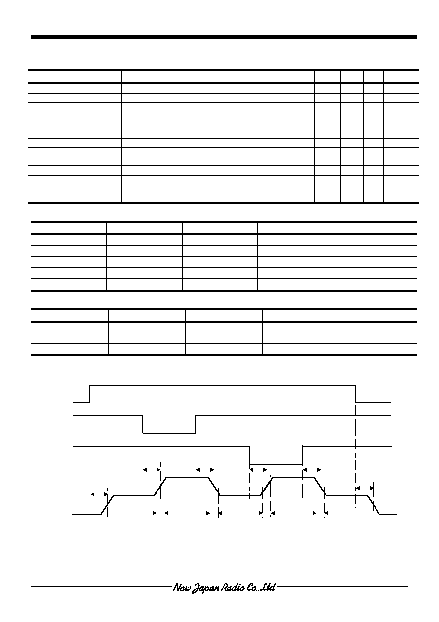
Timing Diaglam
ENABLE
OUTEN2
OUTEN3
Iout
Ten
Tdis
Ton
Toff
Toff
Ton
Tr Tf
Tr
Tf