 | –≠–ª–µ–∫—Ç—Ä–æ–Ω–Ω—ã–π –∫–æ–º–ø–æ–Ω–µ–Ω—Ç: NJW4710 | –°–∫–∞—á–∞—Ç—å:  PDF PDF  ZIP ZIP |
NJW4710
- 1 -
Ver.1
4ch Laser Diode Driver for Blue Laser Diode
s
s
s
s
GENERAL DESCRIPTION
s
s
s
s
PACKAGE OUTLINE
NJW4710 is a laser diode driver for the operation of a grounded
blue laser diode. It is suited to drive a blue laser diode, because it is
operated by split power supply. It includes 4 channels current amplifiers
for 4 different optical power levels. An on-chip RF oscillator is provided
to reduce laser mode noise during read mode. Oscillation frequency
and oscillation amplitude are defined by two external resistors
s
s
s
s
FEATURE
q
Operating Voltage Vcc1=4.5V to 5.5V, Vcc2=8.0 to 10.0V
q
Internal Oscillator Circuit 200MHz to 500MHz
q
Rise Time / Fall Time 0.8ns typ.
q
Maximum Output Current 250mA typ.
q
Bi-CMOS Technology
q
Package Outline SSOP24-E1
s
s
s
s
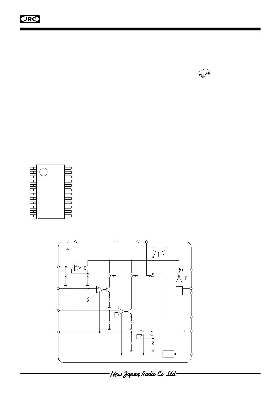
PIN CONFIGURATION
s
s
s
s
BLOCK DIAGRAM
1
12
13
24
1:GND
2:IinR
3:GND
4:Iin2
5:Rfreq
6:Iin3
7:Iin4
8:Vcc1
9:OUTEN2
10:OUTEN3
11:OUTEN4
12:GND
13:GND
14:Vcc2
15:Vcc2
16:OSCEN
17:ENABLE
18:Ramp
19:GND
20:Iout
21:Iout
22:Vcc2
23:Vcc2
24:GND
Vcc1
I
INR
GND
Iout
OSCEN
ENABLE
BIAS
Ramp
OSC
Rfreq
OUTEN2
OUTEN3
OUTEN4
Vcc2
I
IN2
I
IN3
I
IN4
CH-R
CH-2
CH-3
CH-4
NJW4710VE1
NJW4710
- 2 -
Ver.1
s
s
s
s
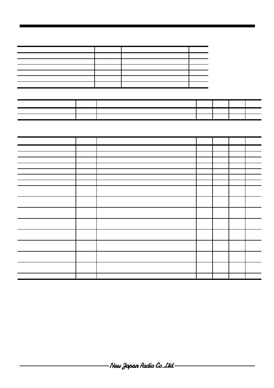
ABSOLUTE MAXIMUM RATINGS(Ta=25
∞
C)
PARAMETER SYMBOL
RATINGS UNIT
Supply Voltage 1
Vcc1
6.0
V
Supply Voltage 2
Vcc2
11.0
V
Input Voltage
Vin
6.0
V
Power Dissipation
P
D
700
mW
Operating Temperature Range
Topr
-40 to +85
∞
C
Storage Temperature Range
Tstg
-40 to +150
∞
C
s
s
s
s
RECOMMENDED OPEARATING CONDITION(Ta=25
∞
C)
PARAMETER SYMBOL
TEST
CONDITION
MIN.
TYP.
MAX.
UNIT
Operating
Voltage1
Vopr1
4.5 5.0 5.5 V
Operating Voltage2
Vopr2
8.0
9.0
10.0
V
s
s
s
s
ELECTRICAL CHARACTERISTICS
q
q
q
q
DC CHARACTERISTICS(Vcc1=5V,Vcc2=9V,ENABLE=H,OUTEN=H,OSCEN=L H:5V,L:GND, Ta=25
∞
C)
PARAMETER SYMBOL
TEST
CONDITION
MIN.
TYP.
MAX.
UNIT
Supply Current 1
I
CC
1
ENABLE
0.5V
- 0 10
mA
Supply Current 2
I
CC
2 IINR/2/3/4=0uA,Rfeq=OPEN,Ramp=OPEN
-
19 24 mA
Supply Current 3
I
CC
3
OSCEN=H, Rfreq=3.6k
,Ramp=5k
- 33 40
mA
Supply Current 4
I
CC
4 OUTEN=H,
IIN/2/3/4=500uA
-
62 76 mA
Supply Current 5
I
CC
5 OUTEN=H,
IINR/2/3/4=500uA
- 120 140 mA
High Level Input Voltage
VIH
OUTEN, OSCEN
2
-
-
V
Low Level Input Voltage
VIL
OUTEN, OSCEN
-
-
1.3
V
ENABLE High Level
Input Voltage
EVIH ENABLE
3
-
-
V
ENABLE Low Level
Input Voltage
EVIL ENABLE
-
-
1.5 V
OUTEN High Level
Input Current
DIIH OUTEN=5V
0
-
10 uA
OUTEN Low Level
Input Current
DIIL OUTEN=0V
-300 -
0 uA
ENABLE High Level
Input Current
EIIH ENABLE=5V
0
- 500 uA
ENABLE Low Level
Input Current
EIIL ENABLE=0V
-10 -
0 uA
OSCEN High Level
Input Current
OIIH OSCEN=5V
0
- 450
uA
OSCEN Low Level
Input Current
OIIL OSCEN=0V
-10 -
0
uA
V
+
1 Shut-Down Voltage
Vshut
3.40
-
3.75
V

NJW4710
- 3 -
Ver.1
q
q
q
q
Laser Amplifier DC CHARACTERISTICS(Vcc1=5V, Vcc2=9V ENABLE=H,H:5V,L:GND,Ta=25
∞
C)
PARAMETER SYMBOL
TEST
CONDITION
MIN.
TYP.
MAX.
UNIT
Current Gain
Gi
CHR/2/3/4, Vo=5V *1
80
110
140
MA
/mA
Output Offset Current
Ios
CHR/2/3/4, Vo=5V *1
-5
-
+5
MA
Output Current Linearity
Iiin
CHR/2/3/4, Vo=5V *1
-3
-
+3
%
Input Current Range 1
Iin1
CHR
0
-
2
MA
Input Current Range 2
Iin2
CH2/3/4
0
-
3.5
MA
Maximum Output Current 1
Iomax1 CHR
50
100
-
MA
Maximum Output Current 2
Iomax2 CH2/3/4
100
200
-
MA
Iout
Series
Resintance
Ro
Iout=200mA
- 10 -
Input Resistance 1
Rin1
CHR
1.62
2.5
3.38
k
Input Resistance 2
Rin2
CH2/3/4
325
500
675
Output OFF Current 1
Ioff1 ENABLE=L
-
-
5 MA
Output OFF Current 2
Ioff2
OUTEN=H, Total for All Channels
-
-
5
MA
Output OFF Current 3
Ioff2 OUTEN=L,
I
IN
=0uA,Total for All Channels
-
-
5
MA
Output Current
Supply Sensitivity 1
Vc1
V
+
1=5V
±
10%, V
+
2=10V
±
10%,Iout=40mA
-1 2 4
%/V
Output Current
Supply Sensitivity 2
Vc2
V
+
1=5V
±
10%, V
+
2=10V
±
10%,Iout=80mA
-1 2 4
%/V
Output Current
Temperature Sensitivity 1
TC1
Iout=40mA,CHR
only
- 400 -
ppm/
∞
C
Output Current
Temperature Sensitivity 2
TC2
Iout=80mA,40mARead+40mA,Write
- 400 -
ppm/
∞
C
*1 The amplifier linearity is calculated using best fit method at three points. The output currents chosen 20 mA,
40mA,and, 60mA.The transfer function for Iout is defined as follows: Iout =(I
IN
+GAIN)+IOS
q
q
q
q
Laser Amplifier AC CHARACTERISTICS (Vcc1=5V, Vcc2=9V,Iout=40mA DC with 40mA PULSE, Ta=25
∞
C)
PARAMETER SYMBOL
TEST
CONDITION
MIN.
TYP.
MAX.
UNIT
Rise Time
Tr
Iout= 40mA(Read)+40mA(10-90%)
-
0.8
-
ns
Fall
Time
Tf Iout=
40mA(Read)+40mA(10-90%)
- 0.8 - ns
Over Shoot
OS
-
5
-
%
Iout ON Time
Ton
OUTEN 50% H
L to Iout 50%
- 1 - ns
Iout OFF Time
Toff
OUTEN 50% H
L to Iout 50%
- 1 - ns
Disable Time
Tdis
ENABLE 50%H
L to Iout 50%
- 20 - ns
Enable Time
Ten
ENABLE 50%L
H to Iout 50%,
- 150 - ns
HFM Disable Time
Tdiso OSCEN H
L to Iout 50%
- 10 - ns
HFM Enable Time
Teno
OSCEN L
H to Iout 50%,
- 10 - ns
Oscillator Frequency
fOSC Rfreq=3.6k
280 350 420
MHz
Oscillator Temperature
Coefficient
TcOSC Rfreq=3.6k
- -300 - ppm/
∞
C
Output Current Noise
Ino
Iout=40mA,CHR only
-
0.9
-
nA/
Hz

NJW4710
- 4 -
Ver.1
s
s
s
s
Iout Control
ENABLE OUTEN2 OUTEN3 OUTEN4
Iout
L/OPEN X
X
X
OFF
H
H/OPEN H/OPEN H/OPEN
Iout=
I
INR
*120
H L
H/OPEN
H/OPEN Iout=(I
INR
+I
IN2
)*120
H L L
H/OPEN
Iout=(I
INR
+I
IN2
+I
IN3
)*120
H L L L Iout=(I
INR
+I
IN2
+I
IN3
+I
IN4
)*120
s
s
s
s
Oscillator Control
ENABLE OSCEN OUTEN2 OUTEN3
OUTEN4
OSCILLATOR
L/OPEN X
X
X X
OFF
H L/OPEN X
X X
OFF
H H X X
X
ON
s
s
s
s
Timing Diagram
Ten
Ton Toff
Tdis
tf
tr
Ton Toff
Ton Toff
tf
tr
tf
tr
Iout
OUTEN4
OUTEN3
OUTEN2
ENABLE
NJW4710
- 5 -
Ver.1
s
s
s
s
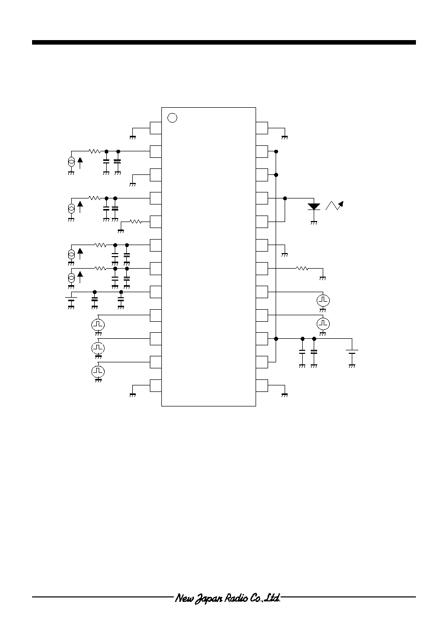
TEST CIRCUIT
2K
1
2
3
4
5
6
7
8
9
10
11
12
13
14
15
16
17
18
19
20
21
22
23
24
2K
2K
2K
5.0K
5V
9V
1u
10u
IinR
0.1u
0.1u
0.1u
Iin2
Iin3
Iin4
1u
10u
LD
GND
IinR
GND
Iin2
Rfreq
Iin3
Iin4
Vcc1
OUTEN2
OUTEN3
OUTEN4
GND
GND
Vcc2
Vcc2
OSCEN
ENABLE
Ramp
GND
Iout
Iout
Vcc2
Vcc2
GND
0.1u
3.6K
TTL/CMOS
TTL/CMOS
TTL/CMOS
TTL/CMOS
CMOS
+
+
0.1u
0.1u
0.1u
0.1u
+
+
+
+

NJW4710
- 6 -
Ver.1
s
s
s
s
TERMINAL EXPLANATION
Pin No.
Pin Name
Function
1
3
12
13
19
24
GND GND
2 IinR
Input of constant current output circuit for Read Channel.
Output current value is set up by input current or input voltage.
4 Iin2
Input of constant current output circuit for Erase, Write Channel.
Output current value is setup by input current or input voltage.
5 Rfreq
Set up for oscillator frequency.
Resistance is connected to GND and a setup in optional frequency.
6 Iin3
Input of constant current output circuit for Erase, Write Channel.
Output current value is setup by input current or input voltage.
7 Iin4
Input of constant current output circuit for Erase, Write Channel.
Output current value is setup by input current or input voltage.
8
Vcc1
Supply voltage for amplifier circuit: Vcc1=5V
9 OUTEN2
Output current control for channel 2
High(<2V) or OPEN: Non-Output
Low(>1.3V): Output
10 OUTEN3
Output current control for channel 3
High(<2V) or OPEN: Non-Output
Low(>1.3V): Output
11 OUTEN4
Output current control for channel 4
High(<2V) or OPEN: Non-Output
Low(>1.3V): Output
14
15
22
23
Vcc2
Supply voltage for output circuit: Vcc2=9V
16 OSCEN
Output control for oscillator.
High(<2V): Oscillation superposition
Low(>1.3V) or OPEN: Non-Output
17 ENABLE
Control for IC.
High(<3V): Output
Low(>1.5V) or OPEN: Non-Output
18 Ranp
Setup for oscillation superposition.
Resistance is connected to GND and a setup in optional oscillation superposition.
20
21
Iout
Output current terminal.
Please connect cathode common type laser or floating type laser to GND.
*Please set up Low voltage not less than GND-0.3V ,and High voltage of each control terminal (ENABLE,
OUTEN 2, 3, and 4, OSCEN) does not exceed Vcc1+0.3V.
NJW4710
- 7 -
Ver.1
Iin
Rex
Rin
Vin
Rex
Rin
Iin
s
s
s
s
APPLICATION
q
q
q
q
Set up for operating voltage
Recommended operating voltage of NJW4710 is Vcc=5V,Vcc=9V.
Vcc2=9V is set up in consideration of the forward voltage [VF] (6V max.) of a Blue Laser Diode.
Therefore, in the case of a Red Laser Diode or Blue Laser Diode with low forward voltage, please set up the
power supply voltage of Vcc2 above the following.
Operating voltage of Vcc2 = forward voltage(MAX) of laser diode + 3V
q
q
q
q
Set up for output current
Current gains of each channels of all are 120mA/mA typ.
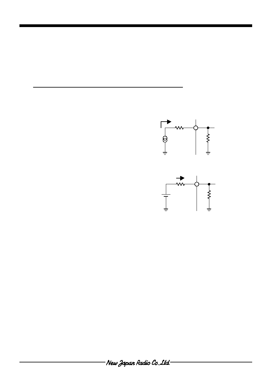
Set up of the output current value in current input and voltage input is below.
In the case of current input
Please input current to IC. Output current is the following.
Iout=120*Iin [mA]
In the case of current input
Output current is the following.
Iout=120*Vin/(Rex+Rin) [mA]
Output current can be set up by Rex=0ohm.
However, to reduce input noise,
please add a capacitor between Rex and GND.
(Refer to TEST CIRCUIT).
Rin(input resistance of IC) is CH-R:2.5kohm,CH-2/3/4:500ohm.
q
q
q
q
Set up for internal Oscillator
NJW4710 contained in the oscillator for the light power change reduction by the return light noise of laser.
The quality of reading improves by operating oscillator and output it.
In this oscillator, oscillation frequency can be set up by connect resistance with a Rfreq(5pin) between GND.
Moreover, set up of the amount of oscillation superposition can be performed by connect resistance with a
Ramp(18pin) between GND.
Oscillation frequency is 150MHz to 600MHz. It can adjust to 10mApp to 100mApp (Refer to TYPCAL
CHARACTERISTICS) in the amount of high frequency superposition.
Output of this oscillator is PUSH-PULL circuit. Therefore, the output of the oscillator for high frequency
superposition is overlapped focusing on the output current value set up in the constant current output circuit.
Fig.2 In the case of current input
Fig.3 In the case of voltage input
NJW4710
- 8 -
Ver.1
0
100
200
300
400
500
600
700
800
0
20
40
60
80
100
120
140
160
0
2
4
6
8
10
12
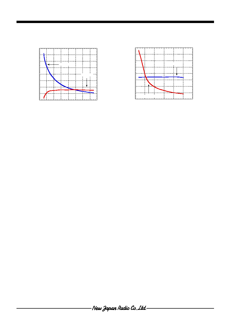
Frequency/Amplitude vs Ramp
Rfreq=3.8K
Fr
e
qency
(
M
H
z
)
A
m
pl
i
t
ude (
m
A
pp)
Ramp (K ohm)
Frequency
Amplitude
Oscillation frequency/Amplitude
vs. Resistance for set up frequency
Oscillation frequency/Amplitude
vs. Resistance for set up overlap
0
100
200
300
400
500
600
700
800
0
20
40
60
80
100
120
140
160
0
2
4
6
8
10
12
14
16
Frequency/Amplitude vs. Rfreq
Ramp=5K
Fr
eque
nc
y (
M
H
z
)
Am
pl
i
t
ude (
m
App
)
Rfreq (K ohm)
Frequency
Amplitude

NJW4710
- 9 -
Ver.1
s
s
s
s
PACKAGE OUTLINE
SSOP24-E1
0. 15
0.10
0. 12
M
1.
1
5
±
0
.
1
0.
1
0
±
0
.
0
5
0.
5
±
0.
2
0 ~ 10∞
- 0. 05
+ 0.1
0. 22 - 0.05
+ 0.1
0. 65
0.375TYP
1
12
13
24
7. 9 ± 0. 2
5.
6
±
0.
2
7.
6
±
0.
2
[CAUTION]
The specifications on this databook are only
given for information , without any
guarantee
as regards either mistakes or omissions. The
application circuits in this databook are
described only to show representative usages
of the product and not intended for the
guarantee or permission of any right