NSVS676 Dec-01
Application
463MHz Low-Loss Type
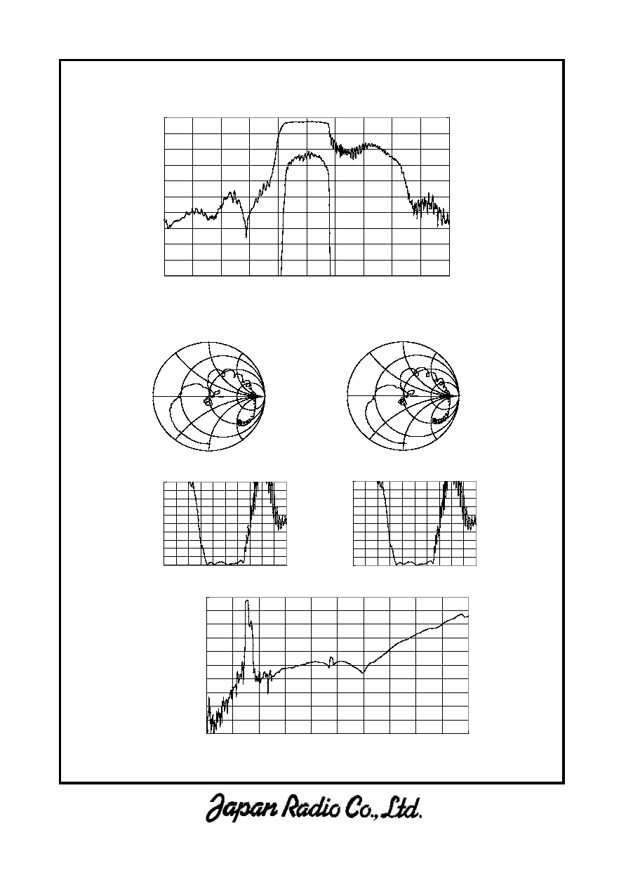
Electrical Specification: (Table 1)
The device characteristics are measured in the circuit shown in Fig.1.
Maximum Rating: (Table 2)
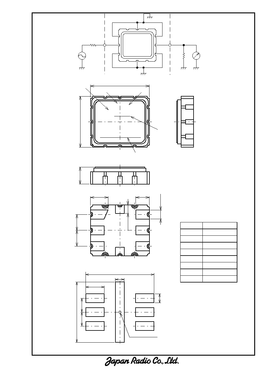
Mechanical Specifications: (Fig.2)
Package is designed as small as 5.2x4.5x1.5[mm
3
] for SMD (Surface Mount Device) type.
Notice:
This part is electrostatic discharge sensitive and may be damaged by improper handling.
Table 1. Electrical Specifications
Item Spec.
Typical
Input and Output Impedance
-
50
Nominal Center Frequency (f0)
-
463MHz
Insertion Loss
453~473MHz
4.0dB max.
2.8dB
Response Variation
453~473MHz
2.0dB max.
0.9dB
Input and Output VSWR
453~473MHz
2.5 max.
1.5
423MHz 40dB
min. 45dB
Out of Band Rejection
(Relative to Through Level)
553MHz 40dB
min. 45dB
(Operating Temperature Range: -10+60�C)
Table 2. Maximum Ratings
Item Rating
Maximum Input Power
+20dBm
Maximum DC Voltage
7.5V
Operating Temperature Range
-10~+60�C
Storage Temperature
-30~+85�C
JRC SAW FILTER
NSVS676
Communications Equipment Division
Communications Equipment Marketing Department
17-22 Akasaka 2-chome minato-ku,
Tokyo. 107-0052 Japan
Tel. +81 3-3584-8811
Fax. +81 3-3584-8876
http://www.jrc.co.jp/product/comm/deveice/saw/saw_top.html (Japanese)
http://www.jrc.co.jp/product/comm/device/saw/saw_top_e.html (English)
NSVS676 Dec-01
Marking
(1) Manufacture's Mark
(2) Lot Number
(a)
Year
(b)
Month
*Oct.---
X
Nov.---
Y
Dec.---
Z
(3) Part number Mark
Pin no.
Connection
1 GND
2 IN/OUT
3 GND
4 GND
5 GND
6 OUT/IN
7 GND
8 GND
5.2�0.2
4.
5
�
0
.
2
1.
5
�
0
.
2
4
3
2
1
5
6
7
8
(1.2)
(1.55)
(
1
.
27)
(1
.2
7
)
(0
.7
5
)
(0
.
8
)
(1)
(a)
(b)
(2)
(3)
[8
x
]
[2
x
]
[5x]
Fig.1 Measuring circuit
Fig.2 Package dimensions (in mm)
Fig.3 Desirable land area (in mm)
J18
676
1
2
3
4
5
6
7
8
SAW
IN
50
OUT
50
1.
2
7
1.
2
7
0.
8
5.
3
1.6
0.8
6.0
Via-Hole(
0.3)
[6x]
[6
x
]
NSVS676 Dec-01
Notice
1. Use this component within operating temperature range. It might not be
satisfied with electrical specification without operating temperature range.
When it is used less than -10�C or more than +60�C, it might be a cause of
degradation or destruction of the component. Even if it endures during a short
time, it causes degradation of qualification.
2. When soldering iron is used, solder with the temperature at the tip of soldering
iron: 350�C max., the time of soldering: 10 seconds max., the power of
soldering iron: 30W max..
3. Notice that the allowed time of soldering with soldering iron is accumulated
time, when soldering is repeated.
4. As rapid temperature change for cleaning after reflow soldering might be a
cause of destruction clean this component after confirming that temperature of
this component goes down to room temperature.
5. Confirm that there are not any influence for qualification to this component in
mounting on PCB when this component is cleaned.
6. As it might be a cause of degradation of destruction to apply static electricity to
this component, do not apply static electricity or excessive voltage while
assembling and measuring. And do not transport this component with bare
hand.
7. As it might be a cause of degradation or destruction to apply D.C. voltage
between each terminal, apply D.C. voltage 7.5V max. in actual circuit.
Note
1. This specification specifies the quality of this component as a single unit. Make
sure that this component is evaluated and confirmed against this specification
when it is mounted to your products.