NT3883
Dot Matrix LCD 80-Channel Driver
1
V2.1 November, 1999
Features
T
Provides 80-channel LCD driver
T
Internal serial to parallel conversion circuits:
40-bit bi-direction shift register
2
80-bit latch
1
80-bit 4-level driver
1
T
Logic circuit supply voltage range: 4.5V - 5.5V
T
LCD driving voltage range (V
DD
- V
EE
): 3.5V to 11V
T
Applicable LCD duty cycle: 1/2 to 1/16
T
Interfaces with a NT3881B/C/D LCD controller
T
LCD bias voltage can be supplied externally
T
Available in 100-pin QFP and in CHIP FORM
General Description
The NT3883 is a dot matrix LCD 80-channel driver
fabricated by low power CMOS technology. This IC
consists of two 40-bit bi-directional shift registers, 80-bit
latch and 80-bit 4-level LCD driver. The NT3883 converts
serial data that are received from the LCD controller, such
as NT3881B/C/D, to parallel data and outputs LCD driving
waveforms to drive LCD. Expansion of character-type
liquid crystal display can be easily obtained according to
the number and structure of characters.
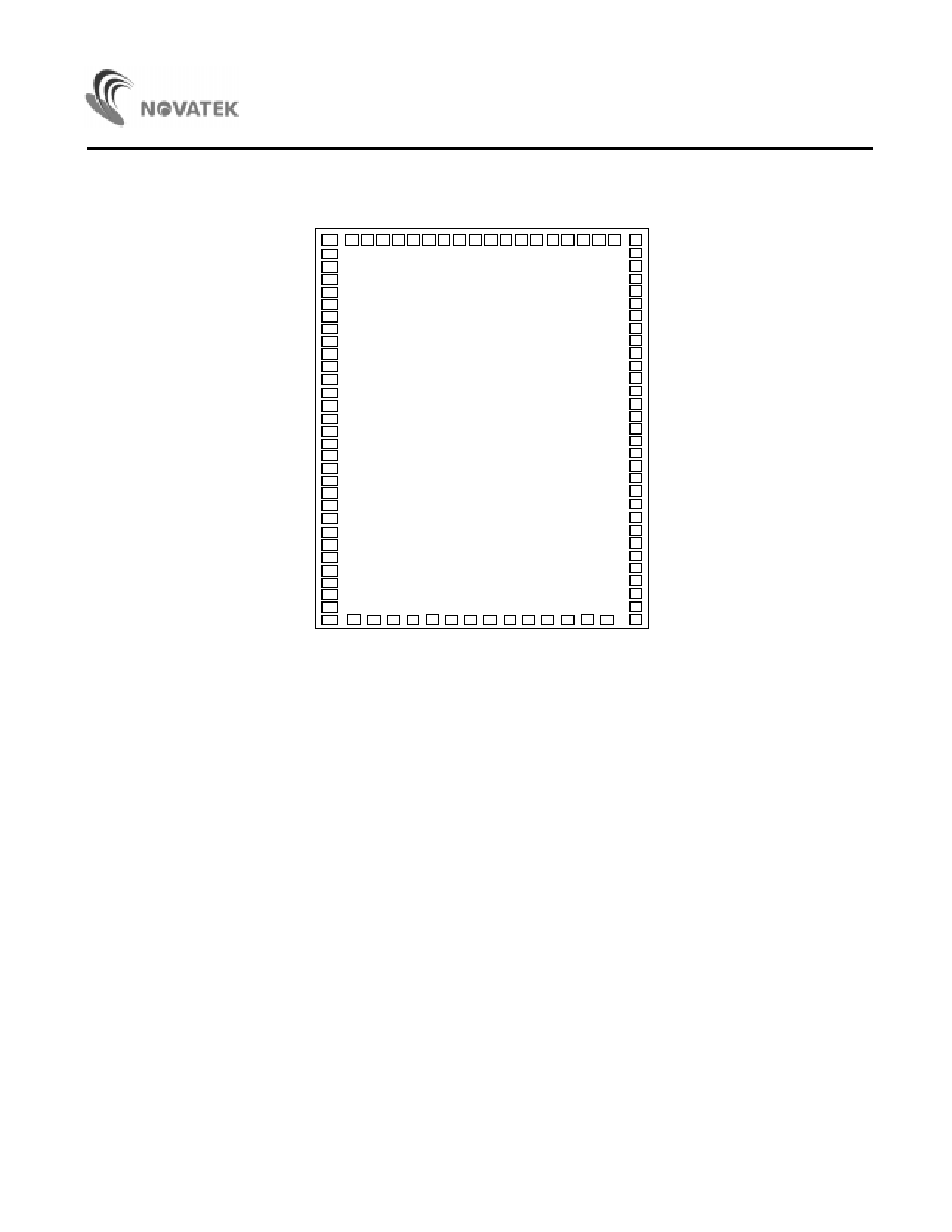
Pin Configuration
100
S
3
1
93
99
92
86
83
81
87
84
98
82
94
96
85
90 89 88
97
91
95
S
7
1
S
7
2
S
7
3
S
7
4
S
7
5
S
7
6
S
7
7
S
7
8
S
7
9
S
8
0
S
4
0
S
3
9
S
3
8
S
3
7
S
3
6
S
3
5
S
3
4
S
3
3
S
3
2
N T 3 8 8 3 F
S18
S19
S20
S21
S22
S23
S24
S25
S26
S27
S28
S29
S30
S3
S4
S5
S6
S7
S8
S9
S10
S11
S12
S13
S14
S15
S16
S17
S1
S2
1
2
18
8
7
11
9
5
6
3
4
10
17
15
16
14
13
12
20
19
27
28
29
30
25
24
23
22
21
26
S58
S59
S60
S61
S62
S63
S64
S65
S66
S67
S68
S69
S70
S43
S44
S45
S46
S47
S48
S49
S50
S51
S52
S53
S54
S55
S56
S57
S41
S42
80
79
63
73
74
70
72
76
75
78
77
71
64
66
65
67
68
69
61
62
54
53
52
51
56
57
58
59
60
55
31
38
32
39
45
48
50
44
47
33
49
37
35
46
41 42 43
34
40
36
V
E
E
N
C
N
C
M
D
R
2
D
L
2
D
R
1
D
L
1
C
L
2
N
C
N
C
N
C
S
L
2
S
L
1
C
L
1
G
N
D
V
2
V
3
V
D
D
N
C
NT3883
4
Absolute Maximum Ratings*
Power Supply Voltage (V
DD
-GND) . . . . . . -0.3V to 7.0V
Power Supply Voltage (V
DD
-V
EE
) . . . . . . . . . . . . . . . . . .
. . . . . . . . . . . . . . . . . . . . . .V
DD
- 13.5V to V
DD
+ 0.3V
Input Voltage . . . . . . . . . . . . . . -0.3V to V
DD
+ 0.3V
Operating Temperature . . . . . . . . . . -20
G
C to + 75
G
C
Storage Temperature . . . . . . . . . . . . . -55
G
C to + 125
G
C
*Comments
Stresses above those listed under "Absolute Maximum
Ratings" may cause permanent damage to this device.
These are stress ratings only. Functional operation of
this device at these or any other conditions above those
indicated in the operational sections of this specification
is not implied and exposure to the absolute maximum
rating conditions for extended periods may affect device
reliability.
DC Electrical Characteristics (V
DD
= 5.0V, GND = 0V, V
EE
= 0V, T
A
= 25
G
C)
Parameter
Symbol
Terminal
Min.
Typ.
Max.
Unit
Conditions
Input Voltage
V
IH
0.7 V
DD
-
V
DD
V
V
IL
CL1, CL2,
DL1, DL2
*1
0
-
0.3 V
DD
V
Output Voltage
V
OH
DR1, DR2
*1
V
DD
- 0.4
-
-
V
I
OH
= -0.4mA
V
OL
-
-
0.4
V
I
OL
= +0.4mA
Vi - Sj Voltage
V
D1
-
-
1.1
V
I
ON
= 0.1mA for one of Sj
Descending
V
D2
*2
-
-
1.5
V
I
ON
= 0.05mA for each of Sj
Input Leakage
Current
I
IL
CL1, CL2
DL1,
DL2*1
-5
-
5
2
A
V
IN
= 0 or V
DD
Vi Leakage
Current
I
VL
V
2
, V
3
, V
EE
-10
-
10
2
A
S1 to S80 open
Power Supply
Current
I
DD
*3
-
-
500
2
A
f
CL1
= 1KHz
f
CL2
= 1MHz
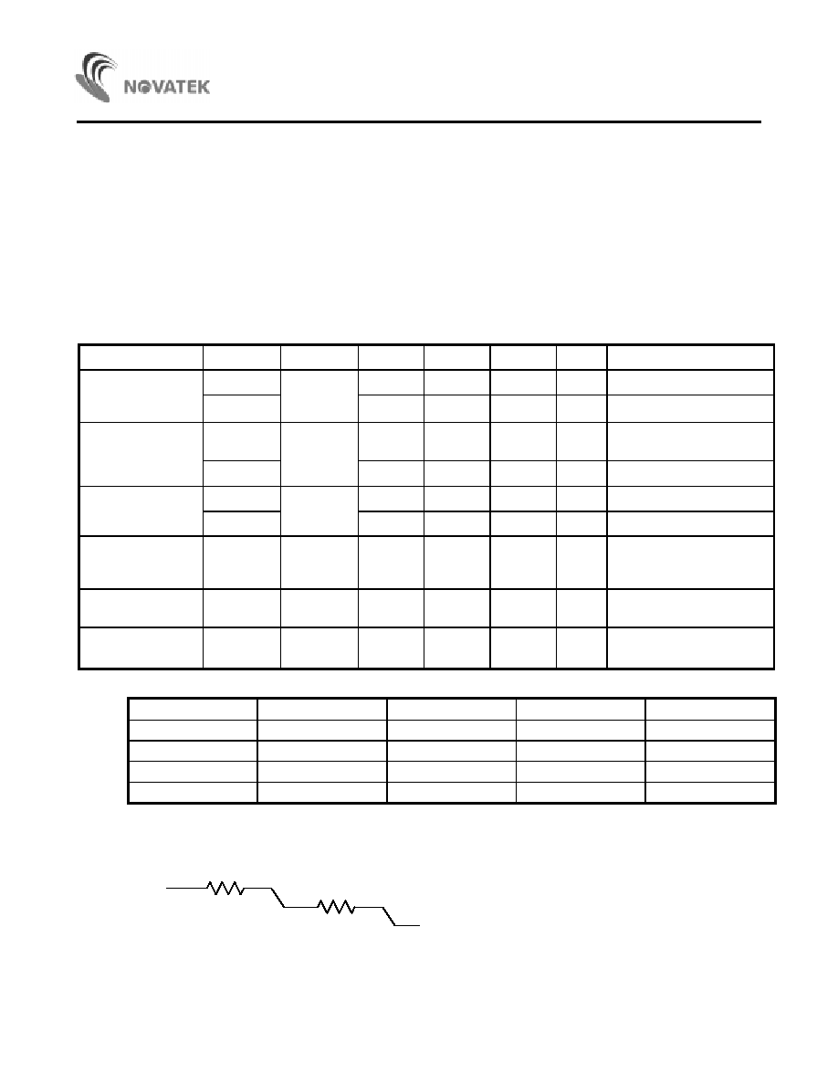
Note *1: SL1 and SL2 determine The Input or Output of DL1, DL2, DR1 and DR2 and the configuration is as follows.
Terminal
SL1 = High
SL1 = Low
SL2 = High
SL2 = Low
DL1
Output
Input
-
-
DR1
Input
Output
-
-
DL2
-
-
Output
Input
DR2
-
-
Input
Output
*2: V
i
� S
j
(V
i
= V
DD
, V
2
, V
3
, V
EE
; j = 1 to 80) equivalent circuit (for reference)
*3: Input/output current is excluded. When the input is at the intermediate level with CMOS, some excessive
V
i
1Kmax.
10Kmax.
Power
Switch
Data
Swtich
S
j
Current will flow through the input circuit to power supply. To avoid this, the input level must be fixed at high or
low state.