 | –≠–ª–µ–∫—Ç—Ä–æ–Ω–Ω—ã–π –∫–æ–º–ø–æ–Ω–µ–Ω—Ç: NT3960 | –°–∫–∞—á–∞—Ç—å:  PDF PDF  ZIP ZIP |
NT3960
TFT LCD Source Driver
1 V1.0
Features
Output : 300/309 output channels
6-bit resolution /64 gray scale
Dot inversion with polarity control
V1 ~ V10 for adjusting Gamma correction
Power for analog circuit : 6.5 ~ 10V
Output dynamic range : 0.1 ~ AV
DD
-0.1V
Power consumption of analog circuit : 2.5mA
Power for interface circuit : 3.0 ~ 3.6V
Operating frequency : 65MHz
Output deviation : 10 ~ 20mV
Data inverting for reducing EMI
Cascade function with bi-direction shift control
CMOS silicon gate ( p-type substrate )
COG
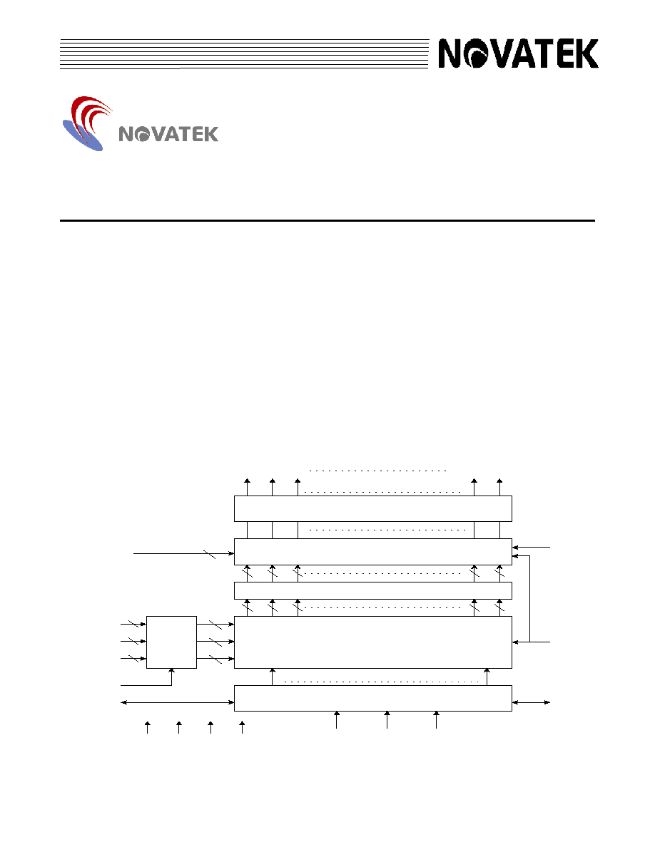
General Description
NT3960 is a data driver IC for a color TFT LCD panel. The channel number of 300 or 309 outputs is selectable for
SVGA and XGA applications. For better performance, dot inversion and a wide range voltage output, 6.5~10V, are designed
in this chip and for reducing EMI, data inversion control is used. This chip also supplies 10 sections of voltage-reference for
Gamma correction.
Block Diagram
Shift Registers ( 103 or 100 )
6
6
6
6
6
D10 ~ D15
6
D00 ~ D05
Decoder
Line Latch ( 309 X 6 bits X 2 )
6
OUT1
6
OUT2
6
OUT3
6
OUT309
6
OUT308
Out Driver Buffer ( 309 channels )
Digital to Analog Converter
1
103
DIO1
DIO2
CLK
SHL
REV
10
V1 ~ V10
LD
D20 ~ D25
Level Shift
6
SELT
POL
Vcc
GND AVDD AVSS
6
6
6
6
NT3960
TFT LCD Source Driver
2
Pin Configuration (IC face view)
PASS1
PASS2
PASS3
DIO2
AVDD
GND
Vcc
DIO1
OUT1
OUT2
OUT3
OUT4
OUT5
OUT309
OUT308
OUT307
OUT306
OUT305
REV
SHL
GND
POL
LD
Test
V10
V9
V8
V7
V6
AVDD
AVSS
V5
V4
V3
V2
V1
NC
CLK
D25
D24
D23
D22
D21
D20
D15
D14
D13
D12
D11
D10
D05
D04
D03
D02
D01
D00
NC
SELT
AVSS
NC
NC
NC
Vcc
GND
AVDD
PASS4
PASS5
PASS6
AVSS
PASS4
PASS5
PASS6
PASS1
PASS2
PASS3
NT3960

NT3960
TFT LCD Source Driver
3
Pad Description
Pad No.
Designation I/O
Description
132~140,142~150,
112~120,122~130,
47~55, 57~65
D05 ~ D00
D15 ~ D10
D25 ~ D20
I
Data input. For three 6-bit data,1 pixel, of color data (R, G, B)
DX5 : MSB; DX0 : LSB
31 ~ 34
REV
I Controls whether data is inverted or not.
When "REV"=1 the data will be inverted. EX. "00" " 3F", "07" " 38", "15" "2A",
and so on.
152 ~ 155
CLK
I Clock signal; latching data onto the line latches at the rising edge.
69 ~ 71
SELT
I Selects the output channel number; when SELT= "0" : 309 channels; and "1" = 300
channels (OUT151~ OUT159 are in-available ). There is a 100K internal pull-up
resistor with this pin.
106 ~ 77
V1 ~ V10
I Gamma correction reference voltage. The voltage of these pins must be AVSS<
V10< V9< V8<V7<V6; V5<V4<V3<V2<V1< AVDD
189 ~ 497
OUT1 ~
OUT309
O Output drive signals;
If 300-channel function is selected, OUT151~ OUT159 are in-available.
Selects left or right shift;
SHL="1" : DIO1 OUT1,2,3 OUT4,5,6 OUT7,8,9--- OUT307,308,309= DIO2
SHL="0" : DIO1=OUT1,2,3 OUT4,5,6 OUT7,8,9 --- OUT307,308,309 DIO2
SHL
DIO1
DIO2
SHIFT
1
Input
Output
Right
35 ~ 37
SHL
I
0 Output
Input Left
176 ~ 178
8 ~ 10
DIO1
DIO2
I/O Start pulse signal input/output
When SHL is applied high (SHL="1"), a start high-pulse on DIO1 is latched at the
rising edge of the CLK. Then the data are latched serially onto internal latches at
the rising edge of the CLK. After all line latches are full with data, 100/103 clocks, a
pulse is shifted out through the DIO2 pin at the rising edge of the CLK. This function
can cascade two or more devices for dot expansion. In normal applications, the
DIO2 signal of the first device is connected to the DIO1 of the second stage, and the
DIO2 of the second one is connected to the DIO1 of the third, and so on like a daisy
chain.
In contrast, when SHL is applied low, a start pulse inputs on DIO2, and outputs
through DIO1.
*Remark : The input pulse-width of DIO1/2 may be over 1 clock-cycle.
44 ~ 46
LD
I Latches the polarity of outputs and switches the new data to outputs.
1. At the rising edge, latches the "POL" signal to control the polarity of the outputs.
2. The pin also controls the switch of the line registers that switches the new
incoming data
to outputs.
*Remark : The LD may switch the new data to outputs at anytime even if the line
data are not completely full.
NT3960
TFT LCD Source Driver
4
Pad Description (continued)
Pad No.
Designation I/O
Description
41 ~ 43
POL
I Polarity select for the dot-inversion control. Available at the rising edge of LD
"POL" value is latched at the rising edge of "LD" to control the polarity of the even or
odd outputs. "POL=1" represents that the next-line odd outputs are of positive
polarity with a voltage output range from V1~V5, and even outputs are of negative
polarity with a voltage output range from V6 to V10. On the other hand, if LD gets
low level "POL", odd outputs are of negative polarity and even outputs are of
positive.
POL=1: Odd outputs range from V1 ~ V5
Even outputs range from V6 ~ V10
POL=0: Odd outputs range from V6 ~ V10
Even outputs range from V1 ~ V5
*Remark: Pay attention to the polarity when selecting the 300-channel function.
The polarity of OUT160 ~OUT309 must be changed. (The polarity needs to
be continuous, +, -, +, -, +, -, etc. If you don't change the polarity, it will not be
continuous between OUT150 and OUT160 when selecting the 300-channel
function. )
11~15, 107~111,
171~175
AVDD
I
Power supply for analog circuits ; 6.5 ~ 10V
16 ~ 20, 72 ~ 76,
166 ~ 170
AVSS
I Ground pins for analog circuits
26 ~ 30, 156 ~ 160
Vcc
I Power supply for digital circuits
21 ~ 25, 38 ~ 40,
161 ~ 165
GND
I Ground pins for digital circuits
66 ~ 68
Test
- For testing
5~7, 500~498
179~181,188~186
PASS1~3
PASS4~6
- The internal connected paths
501, 502
Align Mark
- For COG assembly alignment
1~4, 182 ~ 185,
56, 121, 131, 141,
151
NC -
No
connected
NT3960
TFT LCD Source Driver
5
Power on/off sequence:
This IC is a high-voltage LCD driver, so may be damaged by a large current flow when an incorrect power sequence is used.
First connecting the logical power, Vcc & GND and then the drive power, AVDD&AVSS with V1~V10 as the last is the
recommended sequence. When shutting off the power, first shut off the drive power and then the logic system, or turn off all
power simultaneously.
Relationship between input data and output channels
(1) SHL="1" , shift right, a start pulse from DIO1
Output
OUT1
OUT2
OUT3
- - -
OUT307
OUT308
OUT309
Order
First data
--- Last
data
Data
D05~D00 D15~D10 D25~D20
- - -
D05~D00 D15~D10 D25~D20
(2) SHL="0", shift left, a start pulse from DIO2
Output
OUT1
OUT2
OUT3
- - -
OUT307
OUT308
OUT309
Order
Last data
--- First
data
Data
D05~D00 D15~D10 D25~D20
- - -
D05~D00 D15~D10 D25~D20
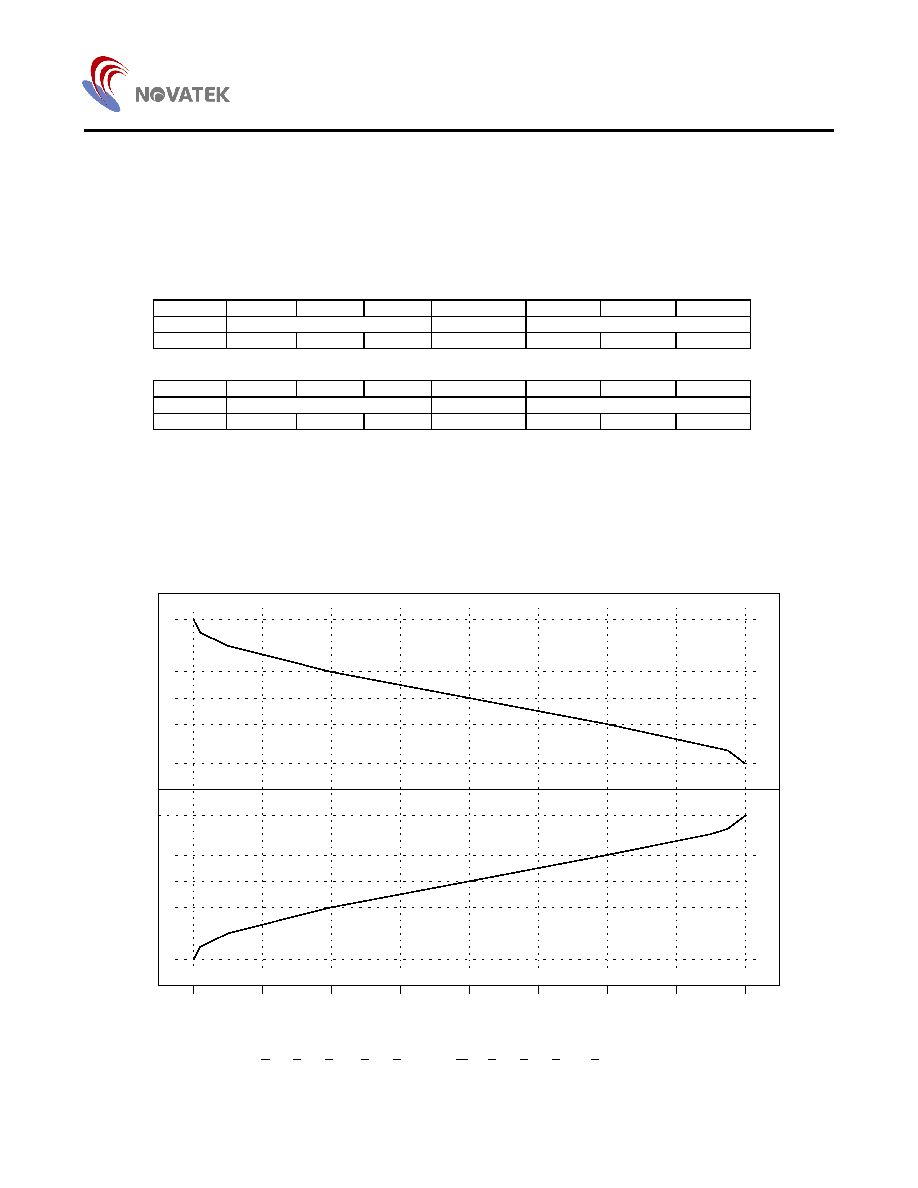
Relationship between input data and output voltage
The figure below shows the relationship between the input data and the output voltage with the polarity. The range of
V1~V5 is for positive polarity, and V6 ~ V10 for negative polarity. Please refer to the following pages to get the relative resistor
value and voltage calculation method.
Remark : AV
DD
-0.1 > V1 > V2 > V3 > V4 > V5 ; V6 > V7 > V8 > V9 > V10 >AVSS+0.1V
Actual application( for reference only): AVD
D
=8.4V, V1=8.2V, V2=7.16V, V3=6.72V, V4=6.38V,
V5=4.98V, V6=3.44V, V7=2.08V, V8=1.70V, V9=1.28V, V10=0.20V.
08H
10H
00H
18H
20H
28H
30H
38H
3FH
V10
V9
V8
V7
V6
Vcom
V5
V4
V3
V2
V1
Gamma correction diagram
Positive polarity
Negative polarity
Input Data
Vout
AVSS
AVDD

NT3960
TFT LCD Source Driver
6
Gamma correction resistor
Name
resistor
R0
2000
R32
150
R1
500
R33
R2
500
R34
R3
500
R35
R4
500
R36
R5
500
R37
R6
500
R38
R7
500
R39
R8
250
R40
R9
250
R41
R10
250
R42
R11
250
R43
R12
250
R44
R13
250
R45
R14
250
R46
R15
250
R47
R16
250
R48
R17
250
R49
R18
200
R50
R19
150
R51
R20
150
R52
R21
150
R53
200
R22
150
R54
250
R23
150
R55
R24
150
R56
R25
150
R57
R26
150
R58
R27
150
R59
500
R28
150
R60
500
R29
150
R61
1250
R30
150
R62
1750
R31
150
Name
resistor
V1, V10
V2, V9
V3, V8
V4, V7
V5, V6
V3, V8
6.10K
2.25K
7.5K
2.65K
Total impedance, Rn=R0 ~ R62, equals 18.5K
150
150
150
150
150
150
100
100
100
150
150
150
150
150
150
150
150
150
150
150
150
250
250
250

NT3960
TFT LCD Source Driver
7
Output Voltage V.S. Input Data
Data Output
Voltage
( Positive polarity )
Output Voltage
( Negative polarity )
00H V1
V10
01H
V2 + ( V1 ≠ V2) X 5500/7500
V10 + ( V9 ≠ V10) X 2000/7500
02H
V2 + ( V1 ≠ V2) X 5000/7500
V10 + ( V9 ≠ V10) X 2500/7500
03H
V2 + ( V1 ≠ V2) X 4500/7500
V10 + ( V9 ≠ V10) X 3000/7500
04H
V2 + ( V1 ≠ V2) X 4000/7500
V10 + ( V9 ≠ V10) X 3500/7500
05H
V2 + ( V1 ≠ V2) X 3500/7500
V10 + ( V9 ≠ V10) X 4000/7500
06H
V2 + ( V1 ≠ V2) X 3000/7500
V10 + ( V9 ≠ V10) X 4500/7500
07H
V2 + ( V1 ≠ V2) X 2500/7500
V10 + ( V9 ≠ V10) X 5000/7500
08H
V2 + ( V1 ≠ V2) X 2000/7500
V10 + ( V9 ≠ V10) X 5500/7500
09H
V2 + ( V1 ≠ V2) X 1750/7500
V10 + ( V9 ≠ V10) X 5750/7500
0AH
V2 + ( V1 ≠ V2) X 1500/7500
V10 + ( V9 ≠ V10) X 6000/7500
0BH
V2 + ( V1 ≠ V2) X 1250/7500
V10 + ( V9 ≠ V10) X 6250/7500
0CH
V2 + ( V1 ≠ V2) X 1000/7500
V10 + ( V9 ≠ V10) X 6500/7500
0DH
V2 + ( V1 ≠ V2) X 750/7500
V10 + ( V9 ≠ V10) X 6750/7500
0EH
V2 + ( V1 ≠ V2) X 500/7500
V10 + ( V9 ≠ V10) X 7000/7500
0FH
V2 + ( V1 ≠ V2) X 250/7500
V10 + ( V9 ≠ V10) X 7250/7500
10H V2
V9
11H
V3 + (V2 ≠ V3) X 2400/2650
V9 + ( V8 ≠ V9) X 250/2650
12H
V3 + (V2 ≠ V3) X 2150/2650
V9 + ( V8 ≠ V9) X 500/2650
13H
V3 + (V2 ≠ V3) X 1950/2650
V9 + ( V8 ≠ V9) X 700/2650
14H
V3 + (V2 ≠ V3) X 1800/2650
V9 + ( V8 ≠ V9) X 850/2650
15H
V3 + (V2 ≠ V3) X 1650/2650
V9 + ( V8 ≠ V9) X 1000/2650
16H
V3 + (V2 ≠ V3) X 1500/2650
V9 + ( V8 ≠ V9) X 1150/2650
17H
V3 + (V2 ≠ V3) X 1350/2650
V9 + ( V8 ≠ V9) X 1300/2650
18H
V3 + (V2 ≠ V3) X 1200/2650
V9 + ( V8 ≠ V9) X 1450/2650
19H
V3 + (V2 ≠ V3) X 1050/2650
V9 + ( V8 ≠ V9) X 1600/2650
1AH
V3 + (V2 ≠ V3) X 900/2650
V9 + ( V8 ≠ V9) X 1750/2650
1BH
V3 + (V2 ≠ V3) X 750/2650
V9 + ( V8 ≠ V9) X 1900/2650
1CH
V3 + (V2 ≠ V3) X 600/2650
V9 + ( V8 ≠ V9) X 2050/2650
1DH
V3 + (V2 ≠ V3) X 450/2650
V9 + ( V8 ≠ V9) X 2200/2650
1EH
V3 + (V2 ≠ V3) X 300/2650
V9 + ( V8 ≠ V9) X 2350/2650
1FH
V3 + (V2 ≠ V3) X 150/2650
V9 + ( V8 ≠ V9) X 2500/2650
20H V3
V8
21H
V4 + (V3 ≠ V4) X 2100/2250
V8 + ( V7 ≠ V8) X 150/2250
22H
V4 + (V3 ≠ V4) X 1950/2250
V8 + ( V7 ≠ V8) X 300/2250
23H
V4 + (V3 ≠ V4) X 1800/2250
V8 + ( V7 ≠ V8) X 450/2250
24H
V4 + (V3 ≠ V4) X 1650/2250
V8 + ( V7 ≠ V8) X 600/2250
25H
V4 + (V3 ≠ V4) X 1500/2250
V8 + ( V7 ≠ V8) X 750/2250
26H
V4 + (V3 ≠ V4) X 1350/2250
V8 + ( V7 ≠ V8) X 900/2250
27H
V4 + (V3 ≠ V4) X 1200/2250
V8 + ( V7 ≠ V8) X 1050/2250
28H
V4 + (V3 ≠ V4) X 1100/2250
V8 + ( V7 ≠ V8) X 1150/2250
29H
V4 + (V3 ≠ V4) X 1000/2250
V8 + ( V7 ≠ V8) X 1250/2250
2AH
V4 + (V3 ≠ V4) X 900/2250
V8 + ( V7 ≠ V8) X 1350/2250
2BH
V4 + (V3 ≠ V4) X 750/2250
V8 + ( V7 ≠ V8) X 1500/2250
2CH
V4 + (V3 ≠ V4) X 600/2250
V8 + ( V7 ≠ V8) X1650/2250
2DH
V4 + (V3 ≠ V4) X 450/2250
V8 + ( V7 ≠ V8) X 1800/2250
2EH
V4 + (V3 ≠ V4) X 300/2250
V8 + ( V7 ≠ V8) X 1950/2250
2FH
V4 + (V3 ≠ V4) X 150/2250
V8 + ( V7 ≠ V8) X 2100/2250

NT3960
TFT LCD Source Driver
8
Output Voltage V.S. Input Data (continued)
Data Output
Voltage
( Positive polarity )
Output Voltage
( Negative polarity )
30H V4
V7
31H
V5 + (V4 ≠ V5) X 5950/6100
V7 + ( V6 ≠ V7) X 150/6100
32H
V5 + (V4 ≠ V5) X 5800/6100
V7 + ( V6 ≠ V7) X 300/6100
33H
V5 + (V4 ≠ V5) X 5650/6100
V7 + ( V6 ≠ V7) X 450/6100
34H
V5 + (V4 ≠ V5) X 5500/6100
V7 + ( V6 ≠ V7) X 600/6100
35H
V5 + (V4 ≠ V5) X 5350/6100
V7 + ( V6 ≠ V7) X 750/6100
36H
V5 + (V4 ≠ V5) X 5200/6100
V7 + ( V6 ≠ V7) X 900/6100
37H
V5 + (V4 ≠ V5) X 5000/6100
V7 + ( V6 ≠ V7) X 1100/6100
38H
V5 + (V4 ≠ V5) X 4750/6100
V7 + ( V6 ≠ V7) X 1350/6100
39H
V5 + (V4 ≠ V5) X 4500/6100
V7 + ( V6 ≠ V7) X 1600/6100
3AH
V5 + (V4 ≠ V5) X 4250/6100
V7 + ( V6 ≠ V7) X 1850/6100
3BH
V5 + (V4 ≠ V5) X 4000/6100
V7 + ( V6 ≠ V7) X 2100/6100
3CH
V5 + (V4 ≠ V5) X 3500/6100
V7 + ( V6 ≠ V7) X 2600/6100
3DH
V5 + (V4 ≠ V5) X 3000/6100
V7 + ( V6 ≠ V7) X 3100/6100
3EH
V5 + (V4 ≠ V5) X 1750/6100
V7 + ( V6 ≠ V7) X 4350/6100
3FH V5
V6

NT3960
TFT LCD Source Driver
9
Absolute
Maximum
Ratings*
*Comments
Logic supply voltage, Vcc
-0.5V to 5V
Supply voltage, AV
DD
-0.5V to +11V
Supply voltage, V1~ V5
0.4AV
DD
~AV
DD
+0.3
Supply range, V6 ~ V10
-0.3 ~ 0.6AV
DD
Storage temperature
-55
0
C to 100
0
C
Operating temperature
-30
0
C to 85
0
C
Stresses above those listed under "Absolute Maximum
Ratings" may cause permanent damage to the device.
These are stress ratings only. Functional operation of this
device at these or under any other conditions above those
indicated in the operational sections of this specification are
not implied and exposure to absolute maximum rating
conditions for extended periods may affect device reliability.
DC Electrical Characteristics
(Vcc =3.3V , AVDD=8.4V, AVSS=GND=0V, TA=-30
0
C ~85
0
C) (For the digital circuit)
Parameter Symbol
Min.
Typ.
Max.
Unit
Conditions
Supply Voltage
Vcc
3
3.3
3.6
V
Digital power
Low Level Input Voltage
Vil
GND
-
0.3xVcc
V
Digital input pins
High Level Input Voltage
Vih
0.7xVcc
-
Vcc
V
Digital input pins
High Level Output Voltage
Voh
Vcc-0.4
-
-
V
DIO1, DIO2, Ioh=1mA
Low Level Output Voltage
Vol
GND
-
GND+0.4 V
DIO1, DIO2, Iol=-1mA
Input Leakage Current
Ii
-
-
±1
µA Digital input pins, SELT exclusive
Pull-up Impedance
Rin
70K
100K
130K
ohm SELT pin
Digital Stand-by Current
Ist
-
10
100
µA
CLK is stopped, SELT is floating
Digital Operating Current
Icc
-
1.5
4
mA
Fclk=65 MHz
(For the analog circuit)
Parameter
Symbol
Min.
Typ.
Max.
Unit
Conditions
Supply Voltage
AVDD
6.5
8.4
10
V
For the analog circuit power
Input level of V1 ~ V5
Vref
0.4AVDD
-
AVDD-0.1
V
Gamma correction voltage
Input level of V6 ~ V10
Vref
0.1
0.6AVDD
V
Gamma correction voltage
-
±
20
±
35
mV
Vo=0.1V ~ 1.5V & AVDD-1.5 ~ AVDD-
0.1V
Voltage Deviation of
Outputs
Vvd
±
15
±
25
mV Vo=1.5V
~
AVDD-1.5V
Dynamic Range of Output
Vdr
0.1
-
AVDD-0.1
V
OUT1 ~ OUT309
Low-Level Output Current
IOL
-100
-150
-
µA
OUT1 ~ OUT309; Vo=0.1V V.S 1.1V
High-Level Output Current
IOH
100
200
-
µA
OUT1 ~ OUT309; Vo=8.3V V.S 7.3V
Impedance of Gamma
Correction
Ri
0.8Rn
1.3Rn
ohm Rn=18.5K, from V1 to V5, V6 to V10
Analog Operating Current
IDD
-
2.5
5
mA
No load, Fclk=33MHz, FLD=50KHz
AC Electrical Characteristics (Vcc =3.0~3.6V , AVDD=8.4V, AVSS=GND=0V, TA= -30~85
0
C
)
Parameter Symbol
Min.
Typ.
Max.
Unit
Conditions
CLK frequency
Fclk - 65
75
Mhz Vcc=3.3V
CLK period cycle
Tcph 13
15
- ns
CLK pulse width
Tcw
4
-
- ns
DIO1/2 set-up time
Tsu
2 -
-
ns
DIO1/2 to CLK
DIO1/2 hold time
Thd
1
-
-
ns
DIO1/2 to CLK
Data set-up time
Tdsu
0 -
-
ns
D00 ~ D25 and REV to CLK
Data hold time
Tdhd
3
-
-
ns
D00 ~ D25 and REV to CLK
Propagation delay of DIO2/1
Tphl
2 -
11 ns
CL=10pF ( Output )
Time that LD leads the last data
Tld
-
-
1
Tcph LD to the last data
Pulse width of LD
Twld
2
-
-
Tcph
POL set-up time
Tpsu
5
-
-
ns
POL to LD
POL hold time
Tphd
2
-
-
ns
POL to LD
Output stable time
Tst
-
-
9
us 96% final value or below with 30mV
precision , CL=60pF, R=10K
Output loading
CL
-
31
150
pF

NT3960
TFT LCD Source Driver
10
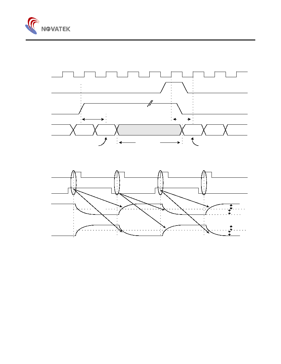
Timing Diagram
CLK
DIO1/2
( Output )
Tcph
Tdsu
Tphl
Tdhd
Tphd
Tst
96%
Data,
REV
Tpsu
POL
Odd outputs
Even outputs
Negative
Positive
Last data
First data
Second data
102
103
DIO1/2
( Input )
LD
Tphl
Tld
Twld
Tst
96%
Vcom
Output
Output load condition :
Tsu
Thd
Tcw
Tcw
LD
2K
20P
4K
20P
4K
20P
High-Z
1
2
NT3960
TFT LCD Source Driver
11
Function operation
CLK
DIO1/2
( Input )
Data,
REV
LD
Odd Outputs
Even Outputs
LD
N-1
N
1
2
POL
Vcom
V6 ~V10
V1 ~V5
V6 ~V10
V1 ~V5
N-2
3
1CLK
1CLK ( max.)
3 CLK (min.)
Last Data
First Data
NT3960
TFT LCD Source Driver
12
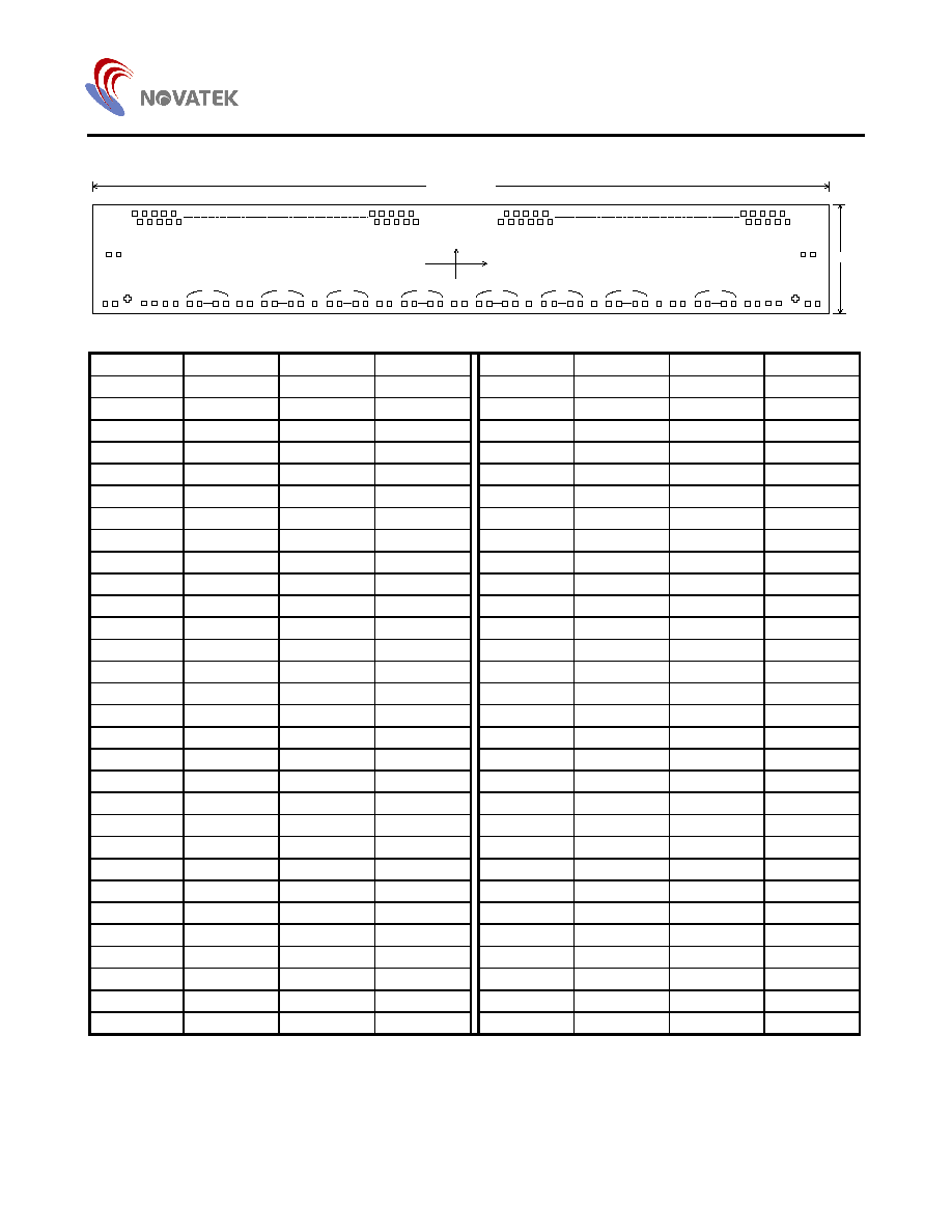
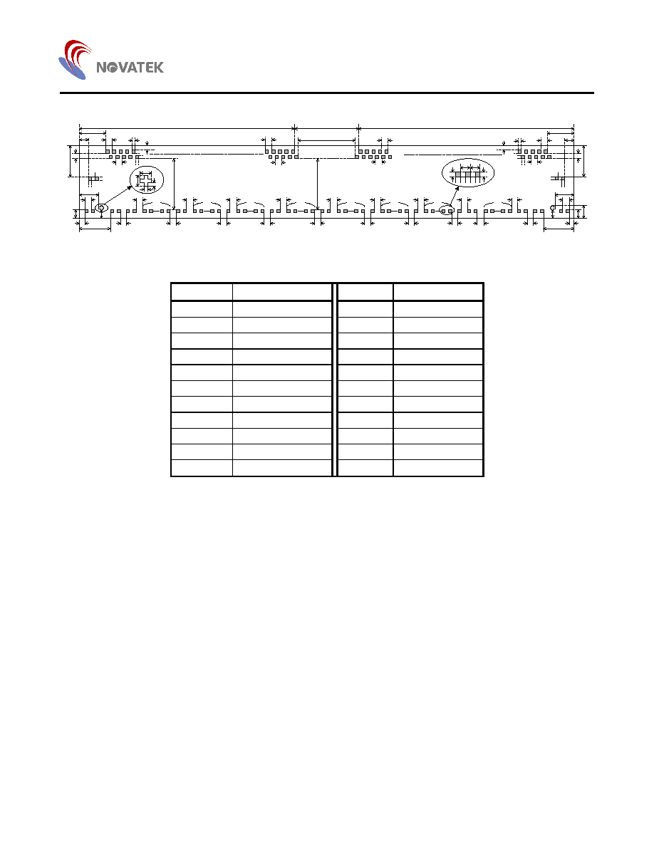
Pad Diagram (Chip size includes the scribe line.)
NT3960
17120
µm
~
~
3
3
3
~
~
5
5
4
~
~
3
3
7
~
~
3
3
5
~
~
3
3
10
~
~
3
3
3
~
~
3
3
3
~
4
~
~
5
5
4
~
4
~
5
~
4
~
3
~
3
~
3
~
3
X
Y
( 0 , 0 )
1110
µm
1
2
3
4
5
7
179 181
182 183
502
184
185
187
186
341
342
344
343
500
499
501
Pad No.
Designation
X
Y
Pad
No.
Designation
X
Y
1
NC -8385 221
31 REV -5810 -427
2
NC -8315 221
32 REV -5740 -427
3
NC -8430 -427
33 REV -5670 -427
4
NC -8360 -427
34 REV -5600 -427
5 PASS1
-8050 -427
35 SHL -5460 -427
6 PASS2
-7980 -427
36 SHL -5390 -427
7 PASS3
-7910 -427
37 SHL -5320 -427
8 DIO2
-7770
-427
38 GND
-5180
-427
9 DIO2
-7700
-427
39 GND
-5110
-427
10 DIO2
-7630 -427
40 GND
-5040 -427
11 AVDD
-7490 -427
41 POL -4900 -427
12 AVDD
-7420 -427
42 POL -4830 -427
13 AVDD
-7350 -427
43 POL -4760 -427
14 AVDD
-7280 -427
44 LD -4620 -427
15 AVDD
-7210 -427
45 LD -4550 -427
16 AVSS
-7070 -427
46 LD -4480 -427
17 AVSS
-7000 -427
47 D25 -4340 -427
18 AVSS
-6930 -427
48 D25 -4270 -427
19 AVSS
-6860 -427
49 D25 -4200 -427
20 AVSS
-6790 -427
50 D24 -4060 -427
21 GND
-6650 -427
51 D24 -3990
-427
22 GND
-6580 -427
52 D24 -3920
-427
23 GND
-6510 -427
53 D23 -3780
-427
24 GND
-6440 -427
54 D23 -3710
-427
25 GND
-6370 -427
55 D23 -3640
-427
26 Vcc
-6230
-427
56 NC -3500
-427
27 Vcc
-6160
-427
57 D22
-3360
-427
28 Vcc
-6090
-427
58 D22
-3290
-427
29 Vcc
-6020
-427
59 D22
-3220
-427
30 Vcc
-5950
-427
60 D21
-3080
-427

NT3960
TFT LCD Source Driver
13
Pad Diagram (continued)
Pad No.
Designation
X
Y
Pad
No.
Designation
X
Y
61 D21
-3010
-427
101 V2 700 -427
62 D21
-2940
-427
102 V2 770 -427
63 D20
-2800
-427
103 V2 840 -427
64 D20
-2730
-427
104 V1 980 -427
65 D20
-2660
-427
105 V1 1050
-427
66 Test
-2520
-427
106 V1 1120 -427
67 Test
-2450
-427
107
AVDD
1260 -427
68 Test
-2380
-427
108
AVDD
1330 -427
69 SELT -2240 -427
109 AVDD 1400 -427
70 SELT -2170 -427
110 AVDD 1470 -427
71 SELT -2100 -427
111 AVDD 1540 -427
72 AVSS
-1960 -427
112 D15 1680 -427
73 AVSS
-1890 -427
113 D15 1750 -427
74 AVSS
-1820 -427
114 D15 1820 -427
75 AVSS
-1750 -427
115 D14 1960 -427
76 AVSS
-1680 -427
116 D14 2030 -427
77 V10
-1540
-427
117 D14 2100
-427
78 V10
-1470
-427
118 D13 2240
-427
79 V10
-1400
-427
119 D13 2310
-427
80 V9
-1260
-427
120 D13
2380
-427
81 V9
-1190
-427
121 NC
2520
-427
82 V9
-1120
-427
122 D12
2660
-427
83 V8 -980
-427
123 D12
2730
-427
84 V8 -910
-427
124 D12
2800
-427
85 V8 -840
-427
125 D11
2940
-427
86 V7 -700
-427
126 D11
3010
-427
87 V7 -630
-427
127 D11
3080
-427
88 V7 -560
-427
128 D10
3220
-427
89 V6 -420
-427
129 D10
3290
-427
90 V6 -350
-427
130 D10
3360
-427
91 V6 -280
-427
131 NC
3500
-427
92 V5 -140
-427
132 D05
3640
-427
93 V5 -70 -427
133 D05
3710
-427
94 V5 0 -427
134 D05
3780
-427
95 V4 140
-427
135 D04
3920
-427
96 V4 210
-427
136 D04
3990
-427
97 V4 280
-427
137 D04
4060
-427
98 V3 420
-427
139 D03
4200
-427
99 V3 490
-427
139 D03
4270
-427
100 V3 560 -427
140 D03 4340
-427
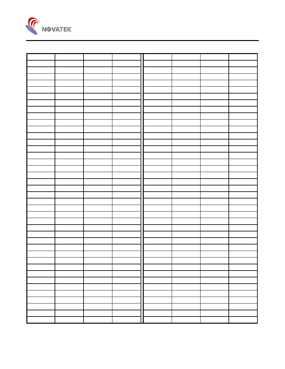
NT3960
TFT LCD Source Driver
14
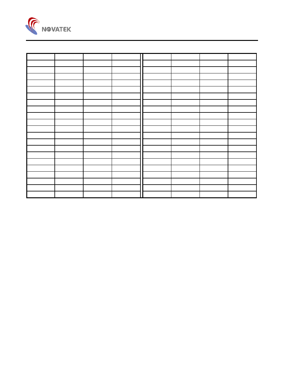
Pad Diagram (continued)
Pad No.
Designation
X
Y
Pad
No.
Designation
X
Y
141 NC 4480 -427
181
PASS6
8050 -427
142 D02 4620 -427
182 NC 8360 -427
143 D02 4690 -427
183 NC 8430 -427
144 D02 4760 -427
184 NC 8315 221
145 D01 4900 -427
185 NC 8385 221
146 D01 4970 -427
186
PASS6
8200 361
147 D01 5040 -427
187
PASS5
8150 431
148 D00 5180 -427
188
PASS4
8100 361
149 D00 5250 -427
189 OUT1
8050 431
150 D00 5320 -427
190 OUT2
8000 361
151 NC 5460 -427
191 OUT3
7950 431
152 CLK 5600 -427
192 OUT4
7900 361
153 CLK 5670 -427
193 OUT5
7850 431
154 CLK 5740 -427
194 OUT6
7800 361
155 CLK 5810 -427
195 OUT7
7750 431
156 Vcc 5950 -427
196 OUT8
7700 361
157 Vcc 6020 -427
197 OUT9
7650 431
158 Vcc 6090 -427
198
OUT10
7600 361
159 Vcc 6160 -427
199
OUT11
7550 431
160 Vcc 6230 -427
200
OUT12
7500 361
161 GND 6370 -427
201 OUT13
7450 431
162 GND 6440 -427
202 OUT14
7400 361
163 GND 6510 -427
203 OUT15
7350 431
164 GND 6580 -427
204 OUT16
7300 361
165 GND 6650 -427
205 OUT17
7250 431
166 AVSS 6790 -427
206 OUT18 7200 361
167 AVSS 6860 -427
207 OUT19 7150 431
168 AVSS 6930 -427
208 OUT20 7100 361
169 AVSS 7000 -427
209 OUT21 7050 431
170 AVSS 7070 -427
210 OUT22 7000 361
171 AVDD 7210 -427
211 OUT23 6950 431
172 AVDD 7280 -427
212 OUT24 6900 361
173 AVDD 7350 -427
213 OUT25 6850 431
174 AVDD 7420 -427
214 OUT26 6800 361
175 AVDD 7490 -427
215 OUT27 6750 431
176 DIO1 7630 -427
216 OUT28
6700 361
177 DIO1 7700 -427
217 OUT29
6650 431
178 DIO1 7770 -427
218 OUT30
6600 361
179 PASS4 7910 -427
219 OUT31 6550 431
180 PASS5 7980 -427
220 OUT32 6500 361

NT3960
TFT LCD Source Driver
15
Pad Diagram (continued)
Pad No.
Designation
X
Y
Pad
No.
Designation
X
Y
221 OUT33 6450 431
261 OUT73 4450 431
222 OUT34 6400 361
262 OUT74 4400 361
223 OUT35 6350 431
263 OUT75 4350 431
224 OUT36 6300 361
264 OUT76 4300 361
225 OUT37 6250 431
265 OUT77 4250 431
226 OUT38 6200 361
266 OUT78 4200 361
227 OUT39 6150 431
267 OUT79 4150 431
228 OUT40 6100 361
268 OUT80 4100 361
229 OUT41 6050 431
269 OUT81 4050 431
230 OUT42 6000 361
270 OUT82 4000 361
231 OUT43 5950 431
271 OUT83 3950 431
232 OUT44 5900 361
272 OUT84 3900 361
233 OUT45 5850 431
273 OUT85 3850 431
234 OUT46 5800 361
274 OUT86 3800 361
235 OUT47 5750 431
275 OUT87 3750 431
236 OUT48 5700 361
276 OUT88 3700 361
237 OUT49 5650 431
277 OUT89 3650 431
238 OUT50 5600 361
278 OUT90 3600 361
239 OUT51 5550 431
279 OUT91 3550 431
240 OUT52 5500 361
280 OUT92 3500 361
241 OUT53 5450 431
281 OUT93 3450 431
242 OUT54 5400 361
282 OUT94 3400 361
243 OUT55 5350 431
283 OUT95 3350 431
244 OUT56 5300 361
284 OUT96 3300 361
245 OUT57 5250 431
285 OUT97 3250 431
246 OUT58 5200 361
286 OUT98 3200 361
247 OUT59 5150 431
287 OUT99 3150 431
248 OUT60 5100 361
288 OUT100 3100 361
249 OUT61 5050 431
289 OUT101 3050 431
250 OUT62 5000 361
290 OUT102 3000 361
251 OUT63 4950 431
291 OUT103 2950 431
252 OUT64 4900 361
292 OUT104 2900 361
253 OUT65 4850 431
293 OUT105 2850 431
254 OUT66 4800 361
294 OUT106 2800 361
255 OUT67 4750 431
295 OUT107 2750 431
256 OUT68 4700 361
296 OUT108 2700 361
257 OUT69 4650 431
297 OUT109 2650 431
258 OUT70 4600 361
298 OUT110 2600 361
259 OUT71 4550 431
299 OUT111 2550 431
260 OUT72 4500 361
300 OUT112 2500 361

NT3960
TFT LCD Source Driver
16
Pad Diagram (continued)
Pad No.
Designation
X
Y
Pad
No.
Designation
X
Y
301 OUT113 2450 431
341 OUT153 450 431
302 OUT114 2400 361
342 OUT154 400 361
303 OUT115 2350 431
343 OUT155 -350 361
304 OUT116 2300 361
344 OUT156 -400 431
305 OUT117 2250 431
345 OUT157 -450 361
306 OUT118 2200 361
346 OUT158 -500 431
307 OUT119 2150 431
347 OUT159 -550 361
308 OUT120 2100 361
348 OUT160 -600 431
309 OUT121 2050 431
349 OUT161 -650 361
310 OUT122 2000 361
350 OUT162 -700 431
311 OUT123 1950 431
351 OUT163 -750 361
312 OUT124 1900 361
352 OUT164 -800 431
313 OUT125 1850 431
353 OUT165 -850 361
314 OUT126 1800 361
354 OUT166 -900 431
315 OUT127 1750 431
355 OUT167 -950 361
316 OUT128 1700 361
356 OUT168 -1000 431
317 OUT129 1650 431
357 OUT169 -1050 361
318 OUT130 1600 361
358 OUT170 -1100 431
319 OUT131 1550 431
359 OUT171 -1150 361
320 OUT132 1500 361
360 OUT172 -1200 431
321 OUT133 1450 431
361 OUT173 -1250 361
322 OUT134 1400 361
362 OUT174 -1300 431
323 OUT135 1350 431
363 OUT175 -1350 361
324 OUT136 1300 361
364 OUT176 -1400 431
325 OUT137 1250 431
365 OUT177 -1450 361
326 OUT138 1200 361
366 OUT178 -1500 431
327 OUT139 1150 431
367 OUT179 -1550 361
328 OUT140 1100 361
368 OUT180 -1600 431
329 OUT141 1050 431
369 OUT181 -1650 361
330 OUT142 1000 361
370 OUT182 -1700 431
331 OUT143 950
431
371 OUT183 -1750 361
332 OUT144 900
361
372 OUT184 -1800 431
333 OUT145 850
431
373 OUT185 -1850 361
334 OUT146 800
361
374 OUT186 -1900 431
335 OUT147 750
431
375 OUT187 -1950 361
336 OUT148 700
361
376 OUT188 -2000 431
337 OUT149 650
431
377 OUT189 -2050 361
338 OUT150 600
361
378 OUT190 -2100 431
339 OUT151 550
431
379 OUT191 -2150 361
340 OUT152 500
361
380 OUT192 -2200 431

NT3960
TFT LCD Source Driver
17
Pad Diagram (continued)
Pad No.
Designation
X
Y
Pad
No.
Designation
X
Y
381 OUT193 -2250 361
421 OUT233 -4250 361
382 OUT194 -2300 431
422 OUT234 -4300 431
383 OUT195 -2350 361
423 OUT235 -4350 361
384 OUT196 -2400 431
424 OUT236 -4400 431
385 OUT197 -2450 361
425 OUT237 -4450 361
386 OUT198 -2500 431
426 OUT238 -4500 431
387 OUT199 -2550 361
427 OUT239 -4550 361
388 OUT200 -2600 431
428 OUT240 -4600 431
389 OUT201 -2650 361
429 OUT241 -4650 361
390 OUT202 -2700 431
430 OUT242 -4700 431
391 OUT203 -2750 361
431 OUT243 -4750 361
392 OUT204 -2800 431
432 OUT244 -4800 431
393 OUT205 -2850 361
433 OUT245 -4850 361
394 OUT206 -2900 431
434 OUT246 -4900 431
395 OUT207 -2950 361
435 OUT247 -4950 361
396 OUT208 -3000 431
436 OUT248 -5000 431
397 OUT209 -3050 361
437 OUT249 -5050 361
398 OUT210 -3100 431
438 OUT250 -5100 431
399 OUT211 -3150 361
439 OUT251 -5150 361
400 OUT212 -3200 431
440 OUT252 -5200 431
401 OUT213 -3250 361
441 OUT253 -5250 361
402 OUT214 -3300 431
442 OUT254 -5300 431
403 OUT215 -3350 361
443 OUT255 -5350 361
404 OUT216 -3400 431
444 OUT256 -5400 431
405 OUT217 -3450 361
445 OUT257 -5450 361
406 OUT218 -3500 431
446 OUT258 -5500 431
407 OUT219 -3550 361
447 OUT259 -5550 361
408 OUT220 -3600 431
448 OUT260 -5600 431
409 OUT221 -3650 361
449 OUT261 -5650 361
410 OUT222 -3700 431
450 OUT262 -5700 431
411 OUT223 -3750 361
451 OUT263 -5750 361
412 OUT224 -3800 431
452 OUT264 -5800 431
413 OUT225 -3850 361
453 OUT265 -5850 361
414 OUT226 -3900 431
454 OUT266 -5900 431
415 OUT227 -3950 361
455 OUT267 -5950 361
416 OUT228 -4000 431
456 OUT268 -6000 431
417 OUT229 -4050 361
457 OUT269 -6050 361
418 OUT230 -4100 431
458 OUT270 -6100 431
419 OUT231 -4150 361
459 OUT271 -6150 361
420 OUT232 -4200 431
460 OUT272 -6200 431
NT3960
TFT LCD Source Driver
18
Pad Diagram (continued)
Pad No.
Designation
X
Y
Pad
No.
Designation
X
Y
461 OUT273 -6250 361
482 OUT294 -7300 431
462 OUT274 -6300 431
483 OUT295 -7350 361
463 OUT275 -6350 361
484 OUT296 -7400 431
464 OUT276 -6400 431
485 OUT297 -7450 361
465 OUT277 -6450 361
486 OUT298 -7500 431
466 OUT278 -6500 431
487 OUT299 -7550 361
467 OUT279 -6550 361
488 OUT300 -7600 431
468 OUT280 -6600 431
489 OUT301 -7650 361
469 OUT281 -6650 361
490 OUT302 -7700 431
470 OUT282 -6700 431
491 OUT303 -7750 361
471 OUT283 -6750 361
492 OUT304 -7800 431
472 OUT284 -6800 431
493 OUT305 -7850 361
473 OUT285 -6850 361
494 OUT306 -7900 431
474 OUT286 -6900 431
495 OUT307 -7950 361
475 OUT287 -6950 361
496 OUT308 -8000 431
476 OUT288 -7000 431
497 OUT309 -8050 361
477 OUT289 -7050 361
498 PASS3 -8100 431
478 OUT290 -7100 431
499 PASS2 -8150 361
479 OUT291 -7150 361
500 PASS1 -8200 431
480 OUT292 -7200 431
501 Align
Mark
-8230 -379
481 OUT293 -7250 361
502 Align
Mark
8230 -379
NT3960
TFT LCD Source Driver
19
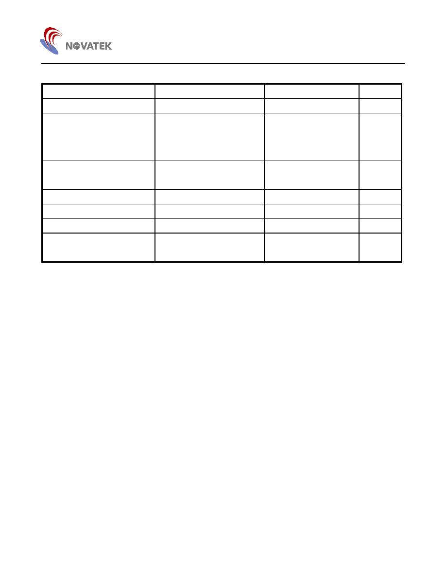
Chip Outline Dimensions
(Bump size)
unit:
µ
µ
µ
µm
~
~
3
3
3
~
~
5
5
4
~
~
3
3
7
~
~
3
3
5
~
~
3
3
10
~
~
3
3
3
~
3
3
~
4
~
~
5
5
4
~
4
~
5
~
4
~
3
~
3
~
3
~
3
A2
A2
A4
Ac
A2
A2
a
a
a
A2
A2
A1
Aa
A1
Aa
B1
B1
B2
B
B3
B2
B
B3
A2
a
B4
C3
C3
C3
C3
C3
C3
C3
C3
C3
C3
C3
C3
C3
C3
C3
C3
C3
C3
C3
C1
C2
C
D1
C1
C2
C
D1
A2
D
D
a
a
a
a
B2
a
a
C2
~
3
C2
C2
a
a
a
a
a
n
n
m
m
a
a
C4
C4
A3
Ab
Symbol
Dimensions in
µ
µ
µ
µm Symbol Dimensions in µµµµm
A1 148.5
B4 221
A2 100
C
483.5
A3 8186.5
C1 103.5
A4 8136.5
C2 70
Aa 333.5
C3 87
Ab 797
C4
285
Ac 697
D
735
B 307.5
D1
131
B1 97.5
a 53
B2 70
m
90
B3 154.5
n 30
NT3960
TFT LCD Source Driver
20
The information of version change
Item
Version 0.2
Version 1.0
Spec. page
AVDD
6.5~11V
6.5~10 V
1, 3, 9
Voltage Deviation of Output
0.1~1.5 & AVDD-0.1~AVDD-1.5V
1.5V ~ AVDD-1.5V
Typ. Max.
±
10
±
20
±
5
±
10
Typ. Max.
±
20
±
35
±
15
±
25
9
Data set-up time/ hold time
Tsu=2nS, Thd=1nS
( base on 0.5Vcc level )
Tdsu=0nS, Tdhd=3nS
( base on Vih level )
9, 10
POL set-up time/ hold time
Tpsu=10nS, Tphd : 5nS (min. )
Tpsu=5nS, Tphd : 2nS (min.)
9
Output current ( IOL, IOH)
-250/250 uA( min. )
-100/100 uA( min.)
9
Propagation delay of DIO2/1
Tphl= 7nS ( Max. )
Tphl= 11nS ( Max.)
9
Chip size
17010 X 1002 um
2
( scribe line exclusive)
17120 X 1110 um
2
( scribe line inclusive)
12, 19