 | –≠–ª–µ–∫—Ç—Ä–æ–Ω–Ω—ã–π –∫–æ–º–ø–æ–Ω–µ–Ω—Ç: NT68275 | –°–∫–∞—á–∞—Ç—å:  PDF PDF  ZIP ZIP |

NT68275
IIC Bus Controlled On-Screen Display
1
V1.0
Features
n
IIC Bus Interface with Slave Address $7A (Transmitter)
& $7B (Receiver)
n
Horizontal Frequency Range: 30KHz ~ 150KHz*
n
Flexible Display Resolution Up to 1524 Dots/Row
n
Internal PLL Generates a Stable and Wide-Ranged
System Clock (120 MHz)*
n
OSD Screen Consist Character Array of 15 Rows by
30 Columns
n
Programmable Vertical and Horizontal Position for
OSD Displaying Center
n
Total of 528* ROM Fonts including 512* Standard &
16 Multi-color ROM Fonts.
n
12 X 18 Dot Matrix Per Character
n
8-Color Selection for Each Character
n
7-Color Selection for Each Character Background
n
Character/Symbol Blinking, Shadowing & Bordering
Display Effect
n
Double Character Height and Width for Each Row
n
Programmable Height of Character/Symbol Display
n
Row To Row Spacing Control to Avoid Expansion
Distortion
n
Four Programmable Windows with Overlapping
Capability and Shadowing Effect
n
Color Setting for Windows' Background and Character
Shadowing & Bordering
n
Fade-In/Out Effect of OSD Screen Display
n
Hsync & Vsync Input Polarity Selectable
General Description
NT68275 is designed for displaying symbols and
characters onto a CRT monitor. Its operation is controlled
by a microcontroller with an IIC bus interface. By sending
proper data and commands to NT68275, it can carry out
the full screen display automatically with the time base
generated by an on-chip PLL circuit. There are many
functions provided by this chip to fully support user
applications, such as: adjustment of the position of OSD
windows, built-in 512* ROM & 16 multi-color fonts,
variable character height with row-to-row spacing
adjustment, 8 color selections & 7 background color
controls for each character, double height/width controls
for each row, 4 overlapping window available with color &
size controls, size controls for each window shadowing,
color selection for windows' shadowing & character
shadowing/ bordering, fade-in/out display effect, etc.
The " * " sign denotes that feature different from NT6827.

NT68275
2
Block Diagram
I
2
C
BUS
R E C E I V E R
S C L
S D A
VSYNC
VFLB
H S Y N C
H F L B
V P O L
H P O L
D I S P L A Y
M E M O R Y
C O N T O L
R E G .
R O M
FONT 12 * 18
O U T P U T
C O N T R O L
R/G/B
F B K G
* P W M / I N T
P O W E R
S Y S T E M
AVCC
P O W E R O N
L O W V O L T A G E
R E S E T
T I M I N G
G E N E R A T O R
DVCC
AGND
DGND
VERTICAL
CONTROL
P L L
C I R C U I T
R P
V C O
HORIZONTAL
CONTROL
BUS CONTROL
BUFFER
DISPLAY
E F F E C T
COLOR
CONTROL
TEST
CIRCUIT
NT68275
3
Pin Assignment
1
2
3
4
5
6
7
8
9
1 0
1 1
1 2
1 6
1 5
1 4
1 3
A G N D
V C O
R P
A V C C
H F L B
N . C .
S D A
S C L
D G N D
R
G
B
F B K G
* P W M C K / I N T
VFLB
D V C C
N T 6 8 2 7 5

NT68275
4
Pin Description
NT68275
NAME
I/O/P/R
Function
1
AGND
P
Analog Ground
2
VCO
-
Voltage I/P to Control Oscillator
3
RP
-
Bias Resistor. Used to bias internal VCO to resonate at specific dot
frequency
4
AVCC
P
Analog Power Supply (5 V Typ.)
5
HFLB
I
Horizontal Fly-back Input (Schmitt Trigger Buffer)
6
N.C.
-
-
7
SDA
I
SDA Pin Of IIC Bus (Schmitt Trigger Buffer) with internal 100K ohm
pulled-high resistance
8
SCL
I
SCL Pin Of IIC Bus (Schmitt Trigger Buffer) with internal 100K ohm
pulled-high resistance
9
DVCC
P
Digital Power Supply (5 V Typ.)
10
VFLB
I
Vertical Fly-back Input (Schmitt Trigger Buffer)
11
*PWMC
K/INT
O
PWM output or Intensity output
12
FBKG
O
Fast Blanking Output. Used to cut off external R, G, B signals.
13
B
O
Blue Color Output with Push-Pull Output Structure
14
G
O
Green Color Output with Push-Pull Output Structure
15
R
O
Red Color Output with Push-Pull Output Structure
16
DGND
P
Digital Ground
NT68275
5
DC/AC Absolute Maximum Ratings*
Recommended Operating Conditions
VCC (measured to GND) . . . . . . . . . .. . 4.75V to 5.25V
Operating Temperature . . . . . . . . . . . . . 0 to +70 0C
*Comments
Stresses above those listed under "Absolute
Maximum Ratings" may cause permanent damage to
this device. These are stress ratings only. Functional
operation of this device at these or any other
conditions above those indicated in the operational
sections of this specification is not implied or
intended. Exposed to the absolute maximum rating
conditions for extended periods may affect device
reliability.
Electrical Characteristics (VDD = 5V, Tamb = 25
∞
C)
Symbol
Parameter
Min. Typ. Max. Unit
Notes
VCC
Supply Voltage
4.75
5
5.25
V
DC Characteristic
Symbol
Parameter
Min. Typ. Max. Unit
Notes
I
DD
Operating Current
22
25
mA
No loading
VIH1
Input High Voltage
2
V
VFLB, HFLB with
Schmitt Trigger Buffer
VIL1
Input Low Voltage
0.8
V
VFLB, HFLB Schmitt
Trigger Buffer
VIH2
IIC Bus Input High Voltage
3
V
VIL2
IIC Bus Input Low Voltage
1.5
V
SCL, SDA
Idrive1
Driving current of R, G, B, FBKG, HFTON
output pins at 2.4V output voltage
80
mA
Isink1
Sinking current of R, G, B, FBKG, HFTON
output pins at 0.4V output voltage
20
mA
Ileak
Leakage current of R, G, B, FBKG pins at
Hi-Z state
10
uA
Measured at 2.5V state
Iiicl
IIC Bus Output Sink Current
5
mA
Viicoutl = 0.4V
Vth
Input Threshold Voltage at HFLB & VFLB 1.8
2.0
2.2
V
VSTIH
Schmitt Trigger Input High Voltage
1.7
2
V
VSTIL
Schmitt Trigger Input Low Voltage
0.8
1.1
V
Refer Figure 1
Iin
Input Current of Hsync, Vsync, SDA, SCL
pins
-10
+10
uA
Schmitt Trigger Buffer

NT68275
6
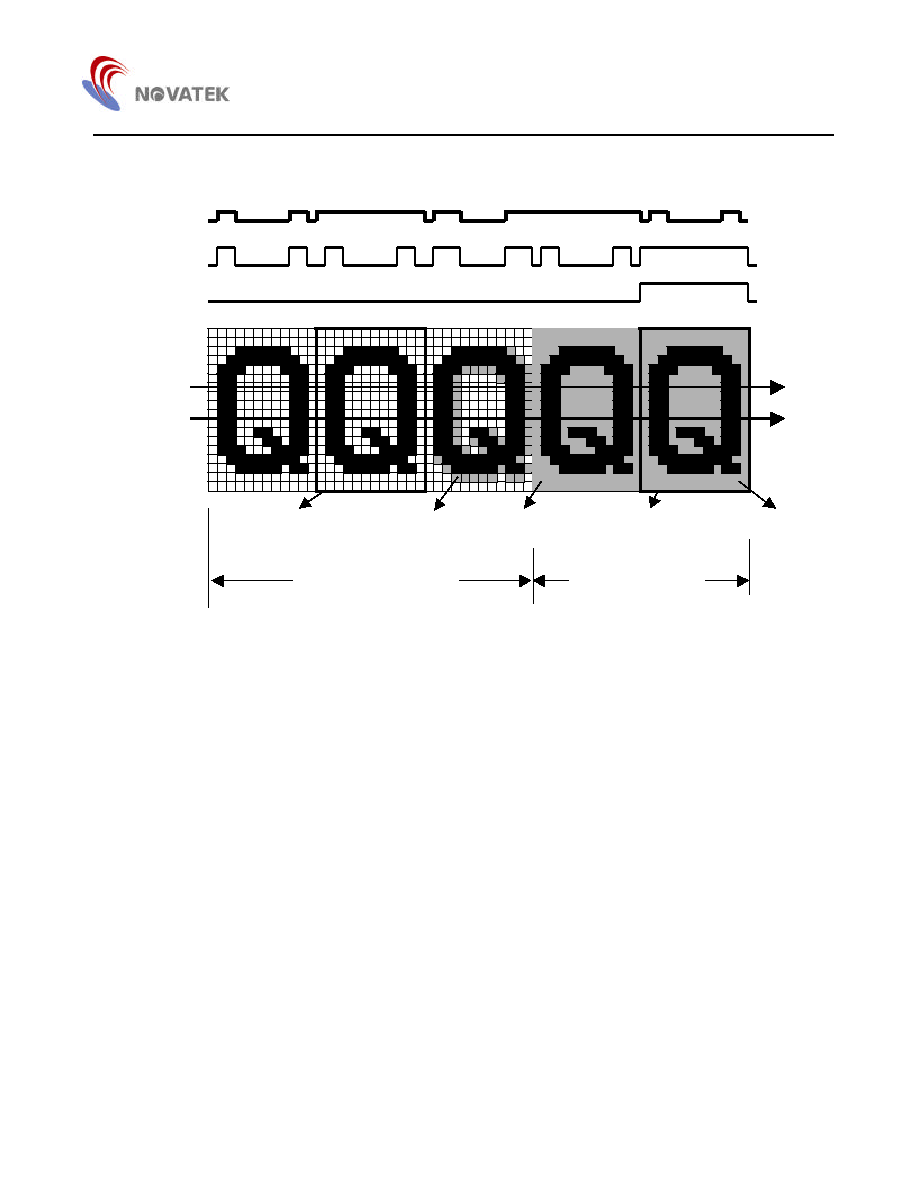
1.1V
1.7V
VH
VL
Output state
Input voltage
Figure 1. Schmitt Trigger Diagram
AC Characteristic
Symbol
Parameter
Min. Typ. Max. Unit
Notes
Fhfy
Horizontal Fly-back Frequency
30
*150
KHz
5
V
Vhfly
Horizontal Fly-back Input
0
V
Thflymin
Minimum Pulse Width of Horizontal Fly-back
0.7
us
Thflymax
Maximum Pulse Width of Horizontal Fly-back
5.5
us
Fvfy
Vertical Fly-back Frequency
50
*200
Hz
5
V
Vvfly
Vertical Fly-back Input
0
V
Tvflymin
Minimum Pulse Width of Vertical Fly-back
20
us
Tvflymax
Maximum Pulse Width of Vertical Fly-back
1
ms
HFLB
2.0 V
Thwidth
0 V
5 V
VFLB
2.0 V
Tvwidth
0 V
5 V
Figure 2. H/V Fly-Back Signal

NT68275
7
NT68275
8
IIC Bus - Slave Transmitter & Receiver (Slave address: $7A & $7B)
Table 1. IIC Bus
Symbol
Parameter
Min.
Typ.
Max.
Unit
Notes
Fmaxcl
Maximum SCL Clock Frequency
100
KHz
VIL
Input Low Voltage
-0.5
1.5
V
VIH
Input High Voltage
3.0
5.5
V
Tlow
Low Period of SCL Clock
4.7
us
Thigh
High Period of SCL Clock
4.0
us
Tsudat
Data Setup Time
250
ns
Thddat
Data Hold Time
300
ns
Tiicr
Rise Time of IIC Bus
1000
ns
Tiicf
Fall Time of IIC Bus
300
ns
Tsusta
Setup Time for Repeated START
Condition
1.3
us
Thdsta
Hold Time for START Condition
4.0
us
Tsusta
Setup Time for START Condition
4.7
us
Tsusto
Setup Time for STOP Condition
4.0
us
SCL, SDA
Tiicbuf
Time IIC bus must be free before next
new transmission can start
4.7
us
Iiicl
IIC Bus Sink Current
4
5
mA
Viicoutl = 0.4 V
Tfilter
Input Filter Spike Suppression
100
ns
SCL, SDA
See also IIC Table Control and IIC Sub Address Control
SCL
SDA
Tiicbuf
Thdsta
Tsudat
Thigh
Tiicr
Tiicf
Thddat
Tlow
STOP START
Tsusta
Thdsta
STOP
Tsusto
START
Figure 3. IIC Bus Timing

NT68275
9
Memory Map
29
14
0
7
0
7
R o w A t t r i b u t e R e g i s t e r
ROW ATTRIBUTE REGISTER
ROW
7
0
30
C O L U M N
0
0
0
DISPLAY REGISTER
F o n t s A d d r e s s $ 0 0 - $ F F
7
Figure 4-1. Memory Map of Display Register (Row 0 ≠ 14)
0
29
14
0
0
7
0
7
C O L U M N
ROW
C H A R A C T E R A T T R I B U T E R E G I S T E R
Character Attribute Register
Figure 4-2. Memory Map of Attribute Register (Row 0 ≠ 14)
NT68275
10
R O W
0
15
0
7
0
7
W i n d o w 1 - 4 C o n t r o l R e g i s t e r
C O L U M N
11
W I N D O W 1 - W I N D O W 4
O S D S C R E E N C O N T R O L
12
22
0
7
0
7
O S D S c r e e n C o n t r o l R e g i s t e r
23
0
7
Reset Flag C o n t r o l R e g i s t e r
Figure 4-3. Memory Map of Control Register (Row 15)
NT68275
11
List of Control Registers:
(1) Display Register: Row 0 ≠ 14 , Column 0 ≠ 29
8
7
6
5
4
3
2
1
0
Row 0-14
Column 0-29
*Page
MSB
LSB
Font's Address $00 - $1FF
Bit 8: * Page -
This bit will address the page 1 ROM font area by bit 7-0 of this control register. Otherwise, it
will address page 0. This can be set by the bit5 column data at IIC bus transmission. Refer to
Figure 8-1 & 8-3 for ROM font area.
Bit 7-0
: These eight bits will address one of the 256 characters/ symbols residing in the character ROM fonts.
Note that if user sets MCFONT bit (row 15, column 22) to `1', the 0 ~ 256 will address standard ROM
fonts, and if cleared to `0', the 0 ~ 239 will address standard ROM fonts & 240 ~ 255, multi-color ROM
fonts.
(2) Character Attribute Register: Row 0 ≠ 14, Column 0 ≠ 29
7
6
5
4
3
2
1
0
Row 0-14
Column 0-29
BKR
BKG
BKB
BLINK
R
G
B
Character Attribute Control
Bit 6-4: BKR/G/B -
These three bits define the color attribute of the background for the corresponding
character/symbol. If all three bits are cleared, no background will be displayed. Refer to the
TAB 3 for the color selections.
Bit 3: BLINK -
This bit enables the blinking effect of the corresponding character/symbol with this bit set to
`1'. The blinking frequency is approximately 1Hz with a fifty-fifty duty cycle at 80Hz vertical sync
frequency.
Bit 2-0: R/G/B -
These three bits define the color attribute of the corresponding character/symbol. Refer to the
TAB 2 for the color selections.
TAB 2. Character/Window Color Selection
COLOR
R
G
B
Black
0
0
0
Blue
0
0
1
Green
0
1
0
Cyan
0
1
1
Red
1
0
0
Magenta
1
0
1
Yellow
1
1
0
White
1
1
1
TAB 3. Character/Window Background Color Selection
COLOR
R
G
B
No Background
0
0
0
Blue
0
0
1
Green
0
1
0
Cyan
0
1
1
Red
1
0
0
Magenta
1
0
1
Yellow
1
1
0
White
1
1
1

NT68275
IIC Bus Controlled On-Screen Display
12
V1.0

NT68275
13
(3) Row Attribute Register: Row 0 ≠ 14, Column 30
7
6
5
4
3
2
1
0
Row 0-14
Column 30
*RINT
DBH
DBW
Row's Attribute Control
Bit 1: DBH
≠ This bit controls the height of the displayed character/symbol. When this bit is set, the
character/symbol is displayed in double height.
Bit 0: DBW
≠ This bit controls the width of the displayed character/symbol. When this bit is set, the
character/symbol is displayed in double width.
Bit 2: * RINT
≠ Row intensity, This bit controls the intensity of the corresponding row .By setting this
bit to 1, the INT pin will go high when the characters of this row are displayed. See Figure 5.
NT68275
14
(4) Window 1 Registers: Row 15, Column 0
7
6
5
4
3
2
1
0
Row Start Address
Row End Address
Row 15
Column 0
MSB
LSB
MSB
LSB
Window 1 Row Size Control
Bit 7-4:
These bits determine the row start position of Window 1on the 15*30 OSD screen.
Bit 3-0:
These bits determine the row end position of Window 1on the 15*30 OSD screen.
7
6
5
4
3
2
1
0
Column Start Address
Row 15
Column 1
MSB
LSB
WINEN *WINT SHAD
Window1 Column Size Control & Attribute Control
Bit 7-3:
These bits determine the column start position of Window 1 on the 15*30 OSD screen.
Bit 2: WINEN -
This bit enables window 1 when it is set. The default value is 0 after power on.
Bit 1: * WINT - Window intensity.
This bit controls the intensity of Window 1 .By setting this bit to 1, the INT pin
will go high while displaying Window 1 and characters inside the window. See Figure 5.
Bit 0: SHAD
- This bit enables the shadowing on the window when it is set to `1'. The default value is 0 after
power on.
7
6
5
4
3
2
1
0
Column End Address
Row 15
Column 2
MSB
LSB
R
G
B
Window 1 Column Size Control & Attribute Control
Bit 7-3:
These bits determine the column end position of Window 1on the 15*30 OSD screen.
Bit 2-0: R/G/B
≠ These bits control the background color of Window 1. Refer to Table for color selection.
Note: Window 1 control registers occupy column 0-2 of row 15, Window 2 from column 3-5, Window 3 from
6-8 and Window 4 from 9-11. The function of Window 2- 4 control registers is the same as Window 1.
Window 1 has the highest priority, and the Window 4, the least. The higher priority color will take
over on the overlap window area.
If the start address of the row/column is greater than the end address, the window will not be
displayed.
Out of range setting (over 15 rows or 30 columns range) will cause abnormal operation.
NT68275
15
OSD Screen Position Control Registers: Row 15, Column 12 - 13
7
6
5
4
3
2
1
0
VPOS
Row 15
Column 12
MSB
LSB
Vertical Position Adjustment
Bit 7-0: VPOS
- These bits determine the vertical starting position for the character display. It is the vertical delay
starting from the leading edge of VFLB. The unit of this setting is 4 horizontal lines and the equation is
defined as below:
Vertical delay = (Vpos * 4 +1) * Horizontal line
. The default value of it is 4 ($04) after power on.
7
6
5
4
3
2
1
0
HPOS
Row 15
Column 13
MSB
LSB
Horizontal Position Adjustment
Bit 7-0: HPOS
≠ These bits determine the horizontal starting position for the character display. It is the
horizontal delay starting from the leading edge of HFLB. The unit of this setting is 6 dots movement shift
to right on the monitor screen and the equation is defined as below:
Horizontal delay = (Hpos * 6 + 49) / P.R.
where the P.R. (pixel rate) is defined by the HDR & Horizontal Frequency.
P.R. (Pixel Rate) = HDR * 12 * Freq
HFLB
Refer the HDR control register at row 15 / column 15 for the P.R. setting.
The default value of these bit is 15 ($ 0F) after power on.
NT68275
16
(5) Character Height Control: Row 15, Column 14
7
6
5
4
3
2
1
0
Row 15
Column 14
CRH6 CRH5 CRH4 CRH3 CRH2 CRH1 CRH0
Character's Height Control
Bit 6-0: CRH6-CRH0
- These bits determine the displayed character height. Character, original 12 by 18 font
matrix, can be expanded from 18 to 71 lines. Refer to the table below. All of these bits will be
cleared to `0' after power on.
If the setting value of CH0 ≠ CH6 is great than 17, the algorithm will repeat at most 17 lines.
TAB 4. Lines Expanded Control
CRH6 ~ CRH0
Lines Inserted
CRH6 = ` 1 ` , CRH5 = ` 1 `
All 18 lines repeat twice
CRH6 = ` 1 ` , CRH5 = ` 0 `
All 18 lines repeat once
CRH6 = ` 0 ` , CRH5 = ` X `
Repeat at most 17 lines
CRH4 = ` 1 `
Insert 16 lines
CRH3 = ` 1 `
Insert 8 lines
CRH2 = ` 1 `
Insert 4 lines
CRH1 = ` 1 `
Insert 2 lines
CRH0 = ` 1 `
Insert 1 lines
TAB 5. Lines Expanded Position
Repeat Position
No. of Lines
Inserted
1 2 3 4 5 6 7 8 9 10 11 12 13 14 15 16 17 18
Insert 1 lines
!
Insert 2 lines
!
!
Insert 4 lines
!
!
!
!
Insert 8 lines
!
!
!
!
!
!
!
!
Insert 16 lines
! ! ! ! ! ! ! ! ! ! ! ! ! ! ! !
Insert 17 lines
! ! ! ! ! ! ! ! ! ! ! ! ! ! ! ! !
NT68275
17
(6) Flexible Display Control Register : Row 15 , Column 15
7
6
5
4
3
2
1
0
HDR
Row 15
Column 15
MSB
LSB
Horizontal Display Resolution Control
Bit 6-0: HDR
-These bits determine the resolution of the horizontal display line. The unit of this setting is
twelve dots (one character). With total 92 steps ($24 ~ $7F: 36 ~ 127 steps; value cannot be smaller
than 36 anytime.), user can adjust the resolution from 36 to 127 characters on each horizontal line.
Note that the resolution adjustment must cooperate with the VCO setting at row 15 / column 18 control
register. Refer to the table of the control register at row 15 / column 18. The default value of it is 40 after
power on.
(7) OSD Row to Row Space Control Register : Row 15 , Column 16
7
6
5
4
3
2
1
0
R2RSPACE
Row 15
Column 16
MSB
LSB
Row To Row Space Adjustment
Bit 4-0: R2RSPACE
- These bits define the row-to-row spacing in units of horizontal lines. Extra lines defined by
this 5-bit value will be appended for each display row. The default value is 0 after power on and there is
no extra line inserted between rows. All of these bits will be cleared to `0' after power on.
(8) Input/Output Control Register : Row 15 , Column 17
7
6
5
4
3
2
1
0
Row 15
Column 17
OSDEN BSEN SHADOW FADE BLANK CLRWIN CLRDSPR FBKGC
OSD Screen Control 1
Bit 7: OSDEN
≠ This bit will enable the OSD circuit when it is set to `1'. The default value is `0' after power on.
Bit 6: BSEN
≠ This bit will enable the bordering and shadowing effect when it is set to `1'. The default value is
`0' after power on.
Bit 5: SHADOW
≠ When the BSEN set to `1', it will enable the shadowing effect when this bit set to `1', too.
Otherwise, it will enable the bordering effect as this bit is cleared to `0'. The default value is `0' after power
on.
Bit 4: FADE
- This bit enables the fade-in/out effect when the OSD screen is turned on by setting from OSDEN
= '0' to `1' or turned off by setting from OSDEN = '1' to `0'. The fade-in/out effect will be completed about
0.5 seconds when the input Vsync is 60 Hz. The default value of this bit is `0' after power on.
Bit 3: BLANK
≠ This bit will force the FBKG pin to output high when this bit & the FBKGOP are bit set to `1'.
Otherwise, the FBKG pin will output low when this bit is set to `1' & FBKGOP bit set to `0'. The default value
of this bit is `0' after power on.
Bit 2: CLRWIN
≠ This bit will clear all windows' WINEN control bit as it is set to `1'. The default value of this bit
is `0' after power on.
Bit 1: CLRDSPR
≠ This bit will clear all of the content in the display registers and R, G, G, BLNK bit in the
character attribute registers when it is set to `1'. The default value of this bit is `0' after power on.

NT68275
18
Bit 0: FBKGC
- It determines the configuration of FBKG output pin. When it is cleared, the FBKG pin will output
high during displaying characters or windows. Otherwise, it will output high only during displaying
characters. The default value of this bit is `0' after power on.

NT68275
19
7
6
5
4
3
2
1
0
Row 15
Column 18 RGBF FBKGOP *PWM/INT DBOUNCE HPOL VPOL VCO1 VCO0
OSD Screen Control 2
Bit 7: RGBF
- This bit controls the driving state of output pins, R, G, B and FBKG when the OSD is disabled.
After power on, this bit is cleared to `0' and all of the R, G, B and FBKG pins output a high impedance
state while the OSD is being disabled. If this bit is set to `1', the R, G, B output pins will drive low, FBKG
pin drive high or low depend on FBKGOP (If FBKGOP=0, drive high. If FBKGOP=1, drive low) while OSD
being disabled.
Bit 6: FBKGOP
- This bit selects the polarity of the output signal of FBKG pin. This signal is active low when the
user clears this bit. Otherwise, active high set this bit. Refer the figure 5 below for the FBKG output timing.
The default value is `1' after power on.
Bit 5: * PWM/INT
- This bit selects the output option to PWM/INT pin. This bit will enable the PWM clock output
as it is set to `1'. Otherwise, it will select the INT option. Refer the figure 5 bellow for the INT output timing.
The default value is `0' after power on.
Bit 4: DBOUNCE
- This bit is to activate the debounce circuit of horizontal and vertical scan. It is to prevent from
the OSD screen shaking when user adjusts the horizontal phase or vertical position. This bit will be
cleared after power on.
Bit 3: HPOL
- This bit selects the polarity of the input signal of horizontal sync (HFLB pin). If the input sync signal
is negative polarity, user must clear this bit. Otherwise, set this bit to `1' to accept the positive polarity
signal. After power on, this bit is cleared to `0' and it will accept negative polarity sync signal.
Bit 2: VPOL
- This bit selects the polarity of the input signal of vertical sync ( VFLB pin). If the input sync signal is
negative polarity, user must clear this bit. Otherwise, set this bit to `1' to accept the positive polarity signal.
After power on, this bit is cleared to `0' and it will accept negative polarity sync signal.
Bit 1-0: VCO1/0 ≠
These bits select the VCO frequency range when user set the horizontal display resolution
flexibly. It is related to the horizontal display resolution and user must set the control register at row15 /
column15 properly. The default value is VCO1=0 & VCO0=0 after power on state. The relationship
between VCO1/0 and display resolution is list below:
TAB 6. P.R. (Pixel Rate) = HDR * 12 * Freq
HFLB
Section
VCO1 VCO0 VCO Freq. Min VCO Freq. Max Unit
P.R. Limit
HFLB Freq. Limit
Freq1
0
0
*6
*13
Freq2
0
1
*14
*28
Freq3
1
0
*29
*60
Freq4
1
1
*61
*120
MHz Min < P.R. < Max
(Min / HDR*12) <
Freq
HFLB
< Max / (HDR*12)
If there are no signals at HFLB input, the PLL will generate an approximate 2.5 MHz clock to ensure the proper
operation of the IIC bus and other control registers.
NT68275
20
Figure 5. * FGBK & INT Output Timing
Window
Backgroun
Window
Backgroun
Character
Backgroun
Character
Backgroun
Character
Shadowin
FBKGC bit = `0'
WINT = 0
FBKGC bit = `1'
WINT = 1
FBK
INT1
RINT=1
RINT=0
INT1
INT2
INT2
NT68275
21
(10) Color Selection for Shadowing/Bordering Effect: Row 15, Column 19
7
6
5
4
3
2
1
0
Row 15
Column 19
WINR WING WINB
CHR
CHG
CHB
Shadowing/Bordering Color Control
Bit 6-4: WINR/G/B
≠ These bits control the shadowing color of window 1-4. Refer to Table 7 for color selection.
All of these bits will be cleared to `0' after power on.
Bit 2-0: CHR/G/B
≠ These bits control the shadowing/bordering color of each character. Refer to Table 7 for
color selection. All of these bits will be cleared to `0' after power on.
TAB 7 Character/Windows' Shadowing Color Selection
COLOR
R
G
B
Black
0
0
0
Blue
0
0
1
Green
0
1
0
Cyan
0
1
1
Red
1
0
0
Magenta
1
0
1
Yellow
1
1
0
White
1
1
1
(11) Multi-Color Font Control: Row 15, Column 20
7
6
5
4
3
2
1
0
Row 15
Column 20
MCFONT
Multi-Color Font Control
Bit 0: MCFONT
≠ This bit will enable multi-color fonts addressed from 240 to 255 when it is set to `1'.
The default value is `0' after power on and enable standard ROM fonts.
NT68275
22
(12) Adjustments of Width & Height for Windows' Shadowing: Row 15, Column 21, 22
7
6
5
4
3
2
1
0
Row 15
Column 21 W4WD1 W4WD0 W3WD1 W3WD0 W2WD1 W2WD0 W1WD1 W1WD0
Setting of Windows' Shadowing Width
WxWD1/0
≠ This will determine the size of window's width when the SHAD bit of windows control register (row
15 column 1,4,7,10) be set to `1'. The default values are `0 0 ` after power on. Refer to the TAB
below for the size adjustments.
WxWD1/0
( 0 , 0 )
( 0 , 1 )
( 1 , 0 )
( 1 , 1 )
Units
Window Shadowing
Width
2
4
6
8
Pixels
7
6
5
4
3
2
1
0
Row 15
Column 22 W4HT1 W4HT0 W3HT1 W3HT0 W2HT1 W2HT0 W1HT1 W1HT0
Setting of Window Shadowing Height
WxHT1/0
≠ These bit will determine the window height when the SHAD bit of the window control register (row 15
column 1,4,7,10) is set to `1'. The default values are `0 0 ` after power on. Refer to the TAB below for
the size adjustments.
WxHT1/0
( 0 , 0 )
( 0 , 1 )
( 1 , 0 )
( 1 , 1 )
Units
Window Shadowing
Height
2
4
6
8
Pixels
NT68275
23
(13) Reset Flag Control Registers
7
6
5
4
3
2
1
0
Row
15
Column
23
RESETFLG
Bit 1: RESTFLG ≠ A system resetwill clear this bit. User can set this bit first and detect if
internal reset circuit has reset the system.
This bit can be read back through IIC bus by external master device, for example MCU.
The other bits are reserved.
(14) Reserved Control Register: Row 15, Column 24 & 31
7
6
5
4
3
2
1
0
Row
15
Column
24
Reserved
This control register is reserved and any data can not be written into this register.
7
6
5
4
3
2
1
0
Row
15
Column
31
Reserved
This control register is reserved and any data can not be written into this register.
IIC Bus Read Mode Operation:
3
---- 1 bytes data ----
4
Type
(1)
(2)
(3)
(4)
(a)
START
Condition
OSD Slave
Address `$7B'
Row15 Column 23
Data
STOP
Condition
8 bits
8 bits
User must read these bytes of data sequentially and can abort transmission by sending NAK (no acknowledge),
Repeat START condition or STOP condition. Every time user sends the START condition (including Repeat
START) and slave address $7B, the NT68275 will respond ACK and then transmit the first byte (content of row5
column3 register). It is prohibited to read more than 1 byte of data.

NT68275
24
IIC Bus Communication:
Figure 6 shows the IIC Bus transmission format.
The master initiates a transmission routine by
generating a START condition, followed by a slave
address byte. Once the address is properly
identified, the slave will respond with an AC-
KNOWLEDGE signal by pulling the SDA line LOW
during the ninth SCL clock. Each data byte which
then follows must be eight bits long, plus the
ACKNOWLEDGE bit, to make up nine bits together.
This ACKNOLEDGE bit is sent by NT68275 at
WRITE mode operation and by master, at READ
mode. In the WRITE mode, appropriate row and
column address information and display data can
be downloaded sequentially from the master in one
of the three transmission formats described in
Figure 6 Access Register Operation. In the READ
mode, the content in some control registers can be
transferred to the master. In the cases of no
ACKNOWLEDGE or completion of data transfer, the
master will generate a STOP condition to terminate
the transmission routine. Note that the OSD_EN bit
must be set after all the display information has
been sent in order to activate the displaying circuitry
of NT68275, so that the received in-formation can
then be displayed.
Write Operation of the Control Registers:
After the proper identification by the receiving
device, a data train of arbitrary length is transmitted
from the master. There are three transmission
formats from (a) to (c) as stated below the Timing
section. The data train in each sequence consists
of row address, column address and data. In
format (a), data must be preceded with the
corresponding row address and column address.
This format is particularly suitable for updating
small amounts of data between different rows.
However, if the current information byte has the
same row address as the one before, format (b) is
recommended. For a full screen pattern change
which requires a massive information update, or
during power up situation, most of the row and
column addresses on either (a) or (b) format will
appear to be redundant. A more efficient data
transmission format (c) should be applied. This
sends the starting row and column addresses
once only, and then treats all subsequent data as
display information. The row and column
addresses will be automatically incremented
internally for each display information data from the
starting location.
To differentiate the row and column addresses
when transferring data from master, the MSB (Most
Significant Bit) is set as in TAB 8 Transmission: `1'
represent row, while `0' for column address.
Furthermore, to distinguish the column address
between format (a), (b) and (c), the sixth bit of the
column address is set to `1', which represents
format (c), and a `0' for format (a) or (b). There is
some limitation on using mix-formats during a
single transmission. It is permissible to change the
format from (a) to (b), or from (a) to (c), or from (b) to
(a), but not from (c) back to (a) or (b).
NT68275
25
IIC Bus Write Operation Timing:
Figure. 6 Access Register Write Operation
3
--------------- Repeat --------------
4
Type
(1)
(2)
(3)
(4)
(5)
(3)
(4)
(5)
(6)
(a)
START
Condition
OSD Slave
Address
`$7A'
Row Address
Data
Column Address
Data
Information
Data
Row Address
Data
Column Address
Data
Information
Data
...
STOP
Condition
8 bits
8 bits
8 bits
8 bits
8 bits
8 bits
8 bits
3
------ Repeat -----
4
Type
(1)
(2)
(3)
(4)
(5)
(4)
(5)
(6)
(b)
START
Condition
OSD Slave
Address
`$7A'
Row Address
Data
Column Address
Data
Information
Data
Column Address
Data
Information
Data
...
STOP
Condition
8 bits
8 bits
8 bits
8 bits
8 bits
8 bits
3
Repeat
4
Type
(1)
(2)
(3)
(4)
(5)
(5)
(5)
(6)
(c)
START
Condition
OSD Slave
Address
`$7A'
Row Address
Data
Column Address
Data
Information
Data
Information
Data
Information
Data
...
STOP
Condition
8 bits
8 bits
8 bits
8 bits
8 bits
8 bits
TAB 8. Address Data Transmission for Registers
ITEM
No
ADDRESS
B7 B6 B5 B4 B3 B2 B1 B0
Type
1
Row
1
0
0
X R3 R2 R1 R0
(a),(b),(c)
2
Column
0
0 *Page C4 C3 C2 C1 C0
(a),(b)
3
Column
0
1 *Page C4 C3 C2 C1 C0
(c)
Display Register
4
Information
Data
D7 D6 D5 D4 D3 D2 D1 D0
5
Row
1
0
1
X R3 R2 R1 R0
(a),(b),(c)
6
Column
0
0
X
C4 C3 C2 C1 C0
(a),(b)
7
Column
0
1
X
C4 C3 C2 C1 C0
(c)
Attribute / Control
Register
8
Information
Data
D7 D6 D5 D4 D3 D2 D1 D0
*The page bit will identify the page number of ROM font area. If this bit is set `0', the following
information data will address the page 0 ROM font area. Otherwise, it will address the page 1.
NT68275
26
Read Operation of the Control Registers:
Not all control registers can be read out by the master via IIC bus of READ mode. Bellow listed, after the proper
identification of slave address ($7B) by the NT68275, 1 byte data train is transmitted to the master.
Item
Register
Bytes
1
Row 15 Column 23 Control Register
1
IIC Bus Read Operation Timing:
Figure 7. Access Register Read Operation
3
---- 1 bytes data ----
4
Type
(1)
(2)
(3)
(4)
(a)
START
Condition
OSD Slave
Address `$7B'
Row15 Column 23
Data
STOP
Condition
8 bits
8 bits
User must read these bytes of data sequentially and can abort transmission by sending NAK (no acknowledge),
Repeat START condition or STOP condition. Every time user sends the START condition (including Repeat START)
and slave address $7B, the NT68275 will respond ACK and then transmit first byte (content of row 15 column 23
register). It is prohibited to read more than 1 byte of data.
NT68275
27
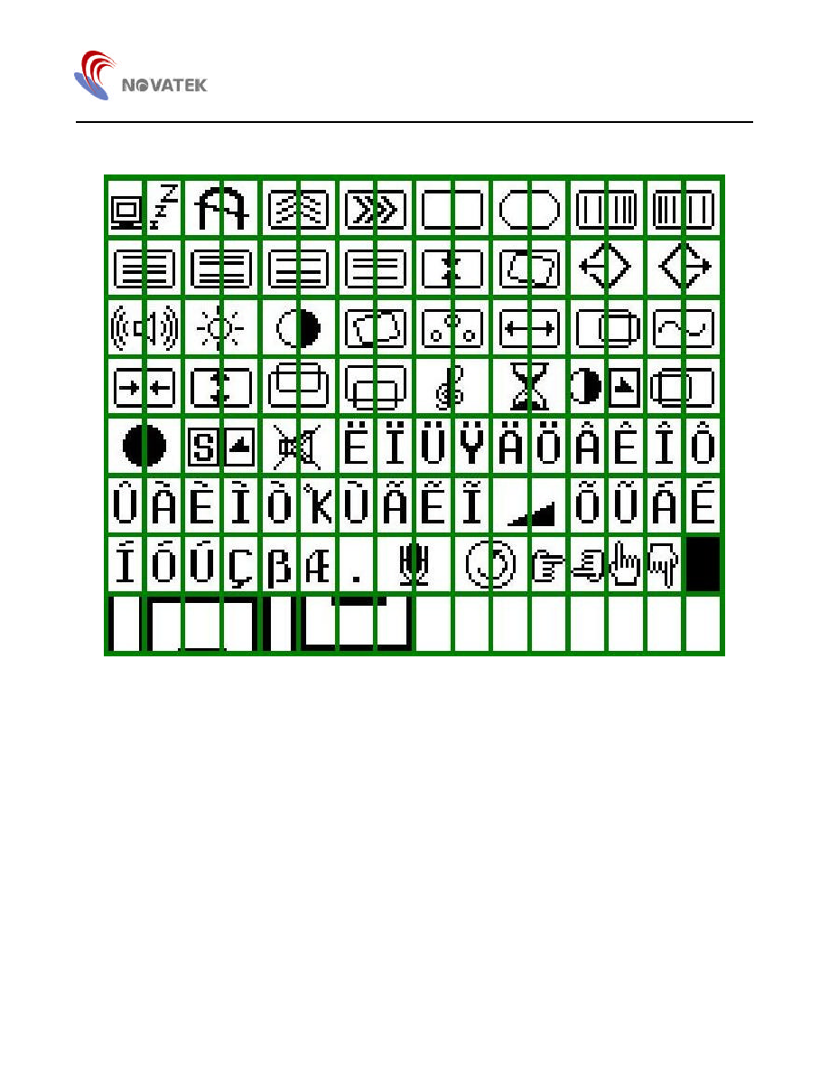
Font Access:
( 00 )
( 01 )
( 02 )
( 03 )
( 04 )
( 05 )
( 06 )
( 07 )
( 08 )
( 09 )
( 0A )
( 0 B )
( 0C )
( 0D )
( 0E )
( 0F )
(10 )
( 11 )
( 12 )
( 13 )
( 14 )
( 15 )
( 16 )
( 17 )
( 18 )
( 19 )
( 1A )
( 1 B )
( 1C )
( 1D )
( 1E )
( 1F )
( 20 )
( 21 )
( 22 )
( 23 )
( 24 )
( 25 )
( 26 )
( 27 )
( 28 )
( 29 )
( 2A )
( 2 B )
( 2C )
( 2D )
( 2E )
( 2F )
( D0 )
( D1 )
( D2 )
( D3 )
( D4 )
( D5 )
( D6 )
( D7 )
( D8 )
( D9 )
( DA )
( DB )
( DC )
( DD )
( DE )
( DF )
( E0 )
( E1 )
( E2 )
( E3 )
( E4 )
( E5 )
( E6 )
( E7 )
( E8 )
( E9 )
( EA )
( EB )
( EC )
( ED )
( EE )
( EF )
( F0 )
( F1 )
( F2 )
( F3 )
( F4 )
( F5 )
( F6 )
( F7 )
( F8 )
( F9 )
( FA )
( FB )
( FC )
( FD )
( FE )
( FF )
.
.
.
R O M F o n t s
Figure 8-1. Page 0 including 256 Standard ROM FONT Configuration
( 00 )
( 01 )
( 02 )
( 03 )
( 04 )
( 05 )
( 06 )
( 07 )
( 08 )
( 09 )
( 0A )
( 0 B )
( 0C )
( 0D )
( 0E )
( 0F )
(10 )
( 11 )
( 12 )
( 13 )
( 14 )
( 15 )
( 16 )
( 17 )
( 18 )
( 19 )
( 1A )
( 1 B )
( 1C )
( 1D )
( 1E )
( 1F )
( 20 )
( 21 )
( 22 )
( 23 )
( 24 )
( 25 )
( 26 )
( 27 )
( 28 )
( 29 )
( 2A )
( 2 B )
( 2C )
( 2D )
( 2E )
( 2F )
( D0 )
( D1 )
( D2 )
( D3 )
( D4 )
( D5 )
( D6 )
( D7 )
( D8 )
( D9 )
( DA )
( DB )
( DC )
( DD )
( DE )
( DF )
( E0 )
( E1 )
( E2 )
( E3 )
( E4 )
( E5 )
( E6 )
( E7 )
( E8 )
( E9 )
( EA )
( EB )
( EC )
( ED )
( EE )
( EF )
( F0 )
( F1 )
( F2 )
( F3 )
( F4 )
( F5 )
( F6 )
( F7 )
( F8 )
( F9 )
( FA )
( FB )
( FC )
( FD )
( FE )
( FF )
.
.
.
R O M F o n t s
M u l t i - c o l o r R O M F o n t s
Figure 8-2. Page 0 including 240 Standard & 16 Multi-color ROM FONT Configuration
NT68275
28
(100 )
( 101 )
( 102 )
( 103 )
(104 )
( 105 )
( 106 )
( 107 )
( 108 )
( 109 )
( 10A )
( 10B ) ( 10 C ) ( 10D ) ( 10 E ) ( 10F )
(110 )
(111 )
( 112 )
( 113 )
( 114 )
( 115 )
( 116 )
( 117 )
( 118 )
( 119 )
( 11A )
( 11B ) ( 11 C ) ( 11D ) ( 11 E ) ( 11F )
( 120 )
( 121 )
( 122 )
( 123 )
( 124 )
( 125 )
( 126 )
( 127 )
( 128 )
( 129 )
( 12A )
( 12B ) ( 12 C ) ( 12D ) ( 12 E ) ( 12F )
( 1D0 ) ( 1D1 )
( 1D2 ) ( 1 D3 ) ( 1D4 ) ( 1 D5 ) ( 1D6 )
( 1D7 ) ( 1D8 )
( 1D9 ) ( 1 DA ) ( 1DB ) ( 1 DC ) ( 1DD ) ( 1 DE ) ( 1DF )
( 1E0 )
( 1E1 )
( 1E2 )
( 1 E3 )
( 1E4 )
( 1 E5 )
( 1E6 )
( 1E7 )
( 1E8 )
( 1E9 )
( 1 EA ) ( 1EB ) ( 1 EC ) ( 1ED ) ( 1 EE ) ( 1EF )
( 1F0 )
( 1F1 )
( 1F2 )
( 1 F3 )
( 1F4 )
( 1 F5 )
( 1F6 )
( 1F7 )
( 1F8 )
( 1F9 )
( 1 FA ) ( 1FB ) ( 1 FC ) ( 1FD ) ( 1 FE ) ( 1FF )
.
.
.
R O M F o n t s
Figure 8 ≠3. * Page 1 including 256 Standard ROM FONT Configuration
NT68275
29
1
2
3
4
5
6
7
8
9
10
11
12
13
14
15
16
17
18
1 2 3 4 5 6 7 8 9 10 1112
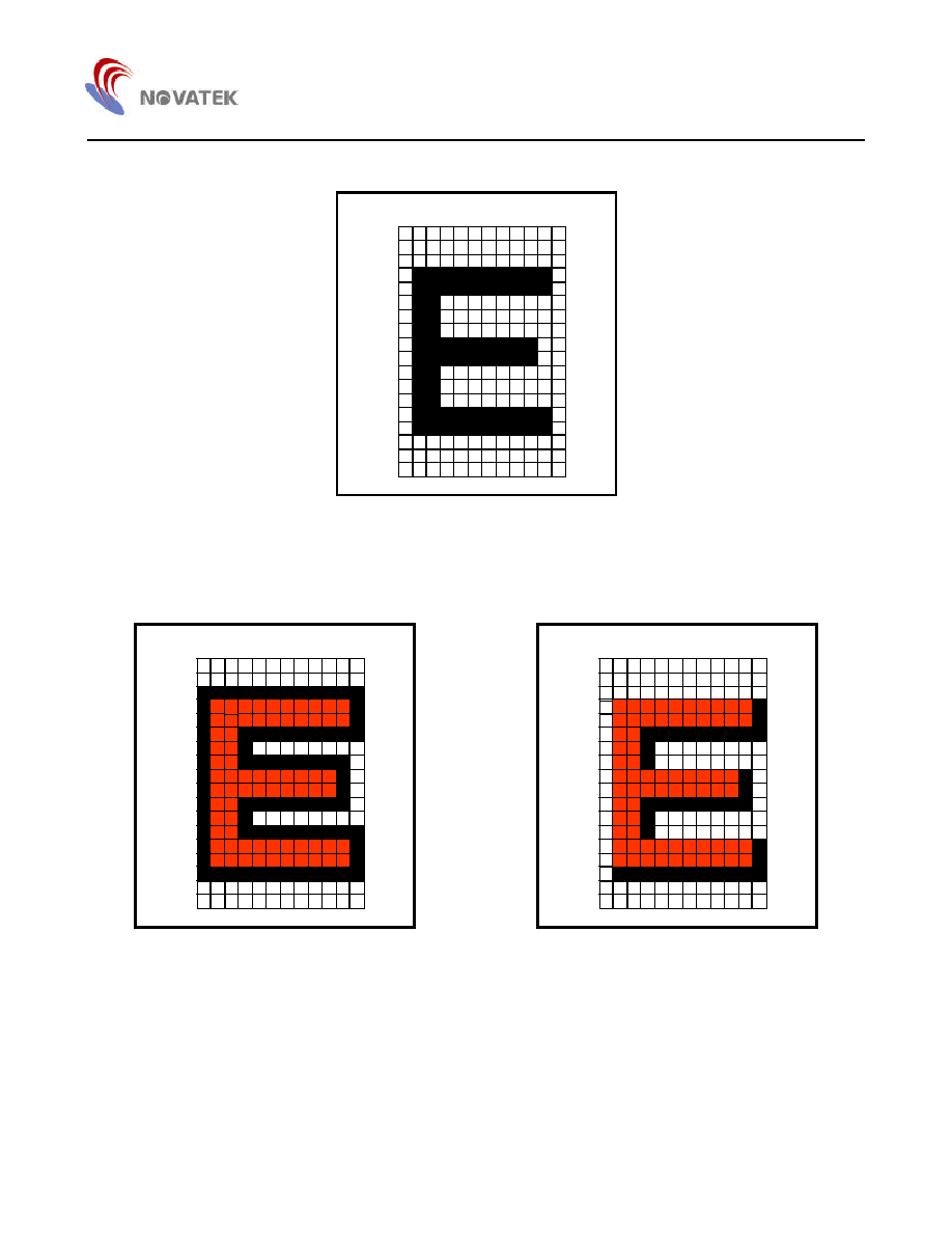
Figure 9-1. 12 * 18 Dots Font
1
2
3
4
5
6
7
8
9
10
11
12
13
14
15
16
17
18
1 2 3 4 5 6 7 8 9 10 1112
1
2
3
4
5
6
7
8
9
10
11
12
13
14
15
16
17
18
1 2 3 4 5 6 7 8 9 10 1112
Figure 9-2. Bordering Effect Figure 9-3. Shadowing Effect
NT68275
30
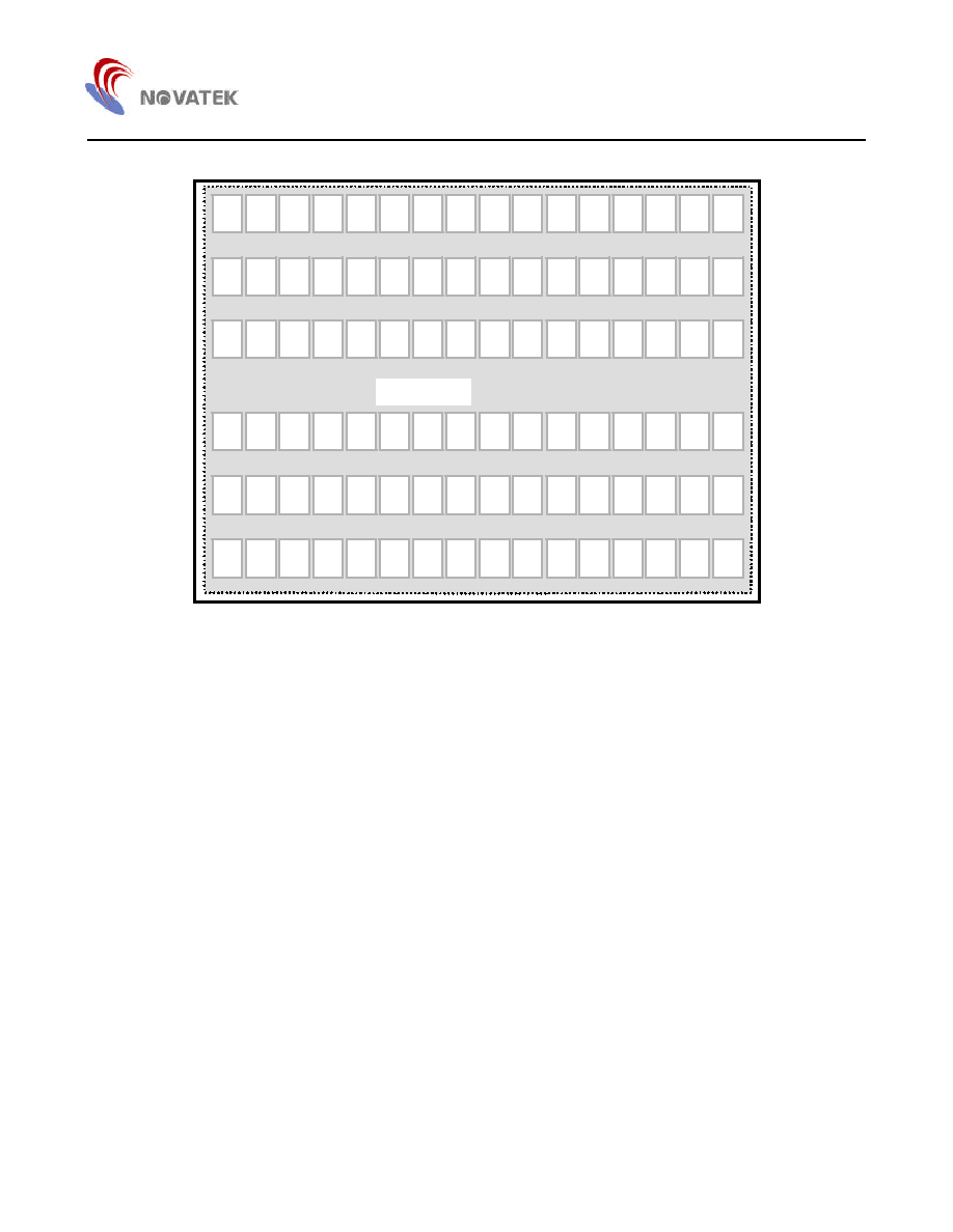
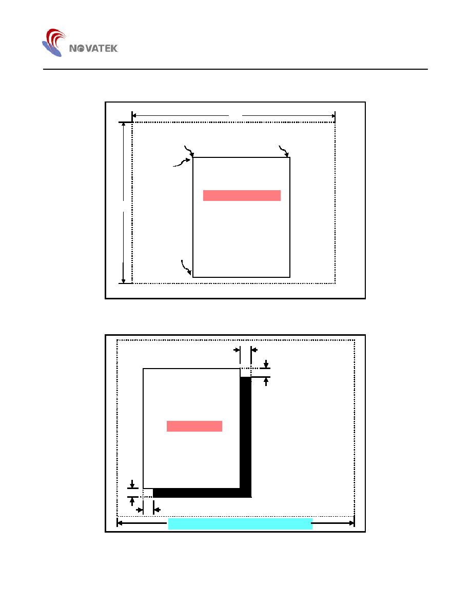
OSD Screen Position:
Figure 10 below illustrates the position of all display characters on the screen relative to the leading edge of
horizontal and vertical fly-back signals.
u
R a s t e r
H F L B
VFLB
O S D
S c r e e n
1 5
30 ( 30*12 =360 Dots )
HPOS *6 + 49 dots
VPOS *4 + 1 lines
VFLB
H F L B
T
T
Figure 10. OSD Screen Position
NT68275
31
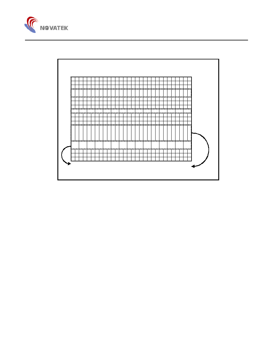
OSD Display Format:
O S D S c r e e n
0 1 2 3 4 5 6 7 8 9 10 11 12 13 14 15 16 17 18 19 20 21 22 23 24 25 26 27 28
0
2
4
6
8
10
12
14
16
18
20
22
24
26
28
Double Height
Double Width
0
1
2
3
4
5
6
7
8
9
10
11
12
13
14
15
Line Expanded = 22 lines
& Double Width
Line Expanded = 22 lines
& Double Height
Figure 11. OSD Display Format
NT68275
32
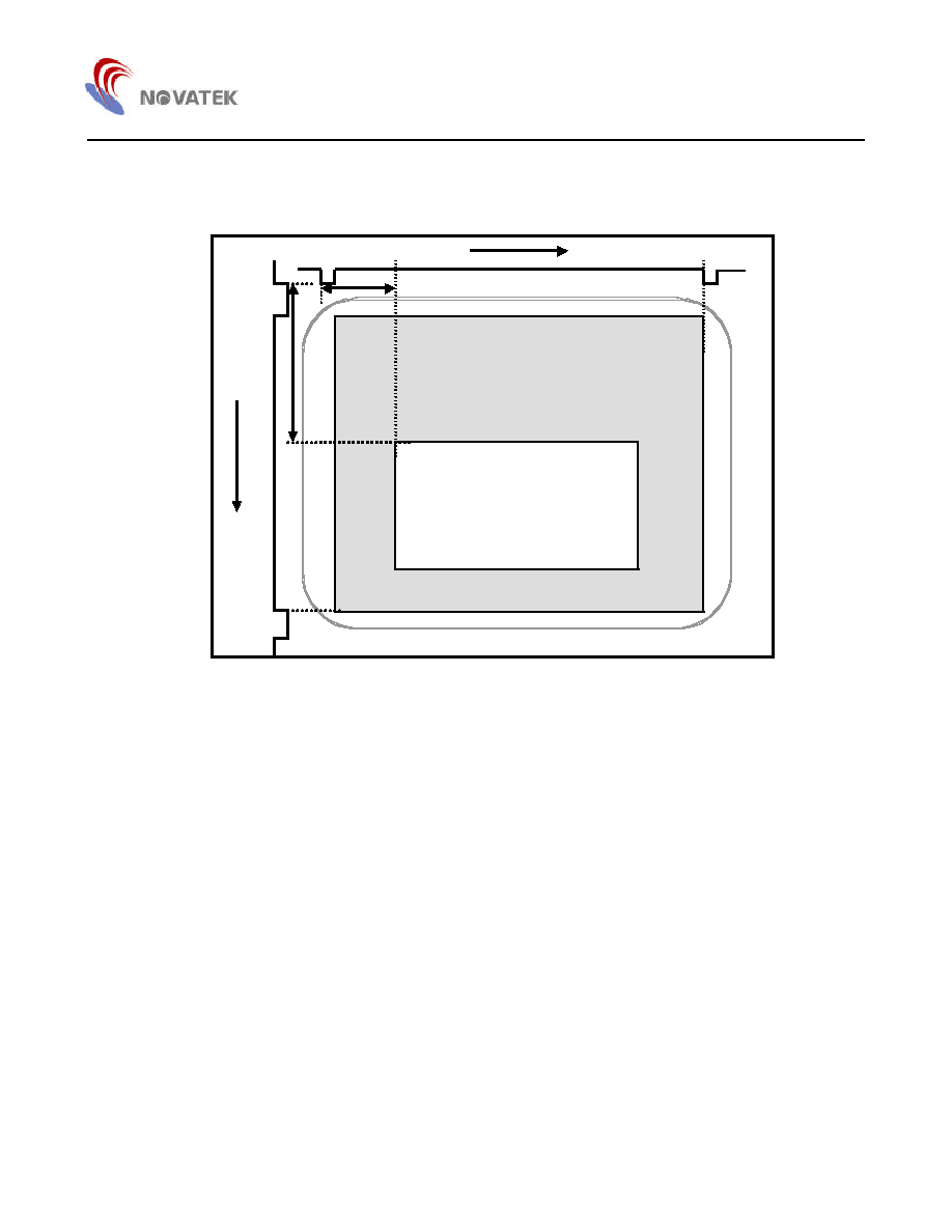
OSD Window Setting:
C o l u m n S t a r t A d d r e s s
Row End Address
Row Start Address
15
30
W I N D O W 1 / 2 / 3 / 4 A R E A
Row Start/End Control Register:
row15 /column 0/3/6/9
Column Start Control Register:
row15 /column 1/4/7/10
C o l u m n E n d C o n t r o l R e g i s t e r :
row15 /column 2/5/8/11
W i n d o w C o l o r C o n t r o l R e g i s t e r :
row15 /column 2/5/8/11
C o l u m n E n d A d d r e s s
Figure 12. Window Size Setting
W I N D O W A R E A
W I D T H
H E I G H T
H E I G H T
W I D T H
W i d t h A d j u s t m e n t C o n t r o l R e g i s t e r:
r o w 1 5 /column 2 1
Height Adjustment Control R e g i s t e r:
r o w 1 5 /column 2 2
Shadow ColorSelection Control R e g i s t e r:
r o w 1 5 /column 1 9
Note : Width Adjustment Units : Pixels
Height Adjustment Units : H Lines
O S D S C R E E N A R E A ( 1 5 r o w b y 3 0 c o l u m n )
Figure 13. Window Shadowing Setting
NT68275
33
Characters' Programmable Height:
TAB 9. Line Expanded
Example 1: If user sets CRH0 = 1, CRH2= 1, CRH3= 1
Line
1 2 3 4 5 6 7 8 9 10 11 12 13 14 15 16 17 18
Original Font
! ! ! ! ! ! ! ! ! ! ! ! ! ! ! ! ! !
CRH0
!
CRH2
!
!
!
!
CRH3
!
!
!
!
!
!
!
!
CH4 ≠ CH 0 <= 18 ! ! ! ! ! ! ! ! ! ! ! ! !
Result : 31 lines
18+ 8*CRH3+4*CRH2
+CRH0
! !! !! !! ! !! !! !! !! !! !! !! ! !! !! !! ! !
Example 2: If user sets CRH0 = 1, CRH 3= 1, CRH4 = 1
Line
1 2 3 4 5 6 7 8 9 10 11 12 13 14 15 16 17 18
Original Font
! ! ! ! ! ! ! ! ! ! ! ! ! ! ! ! ! !
CRH0
!
CRH3
!
!
!
!
!
!
!
!
CRH4
! ! ! ! ! ! ! ! ! ! ! ! ! ! ! !
CH4 ≠ CH 0 >= 18 ! ! ! ! ! ! ! ! ! ! ! ! ! ! ! ! !
Result : 35 lines
18+17
!! !! !! !! !! !! !! !! !! !! !! !! !! !! !! !! !! !
Example 3: If user sets CRH1 = 1, CRH3 = 1, CH5 = 0, CH6 = 1
Line
1 2 3 4 5 6 7 8 9 10 11 12 13 14 15 16 17 18
Original Font
! ! ! ! ! ! ! ! ! ! ! ! ! ! ! ! ! !
CRH1
!
!
CRH3
!
!
!
!
!
!
!
!
CH4 ≠ CH0 < 18
!
! ! !
!
!
! ! !
!
CRH6,5=(1,0)
! ! ! ! ! ! ! ! ! ! ! ! ! ! ! ! ! !
Result : 46 lines
18+( 8 * CRH3 ) +
(2*CRH1)+ 18 * 1
!! !!! !! !!! !!! !!! !! !!! !! !!! !! !!! !!! !!! !! !!! !! !!
NT68275
34
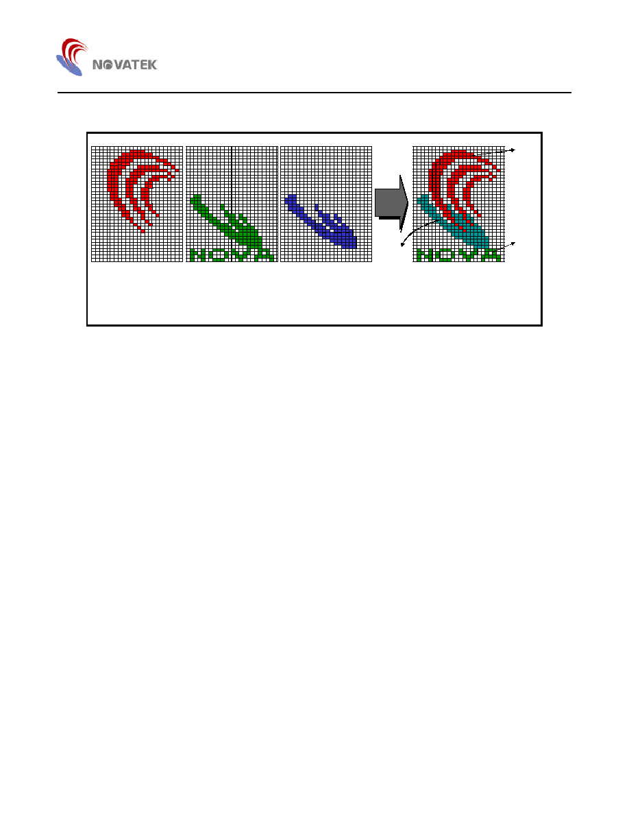
Multi-color Font Operation:
M u l t i - c o l o r F o n t
R
G
B
O / P
G r e e n
C y a n
R e d
Figure 14. Multi-Color Font
Example above, the NOVATEK logo is consisted of four fonts. The R, G, B output channels will send out their
corresponding font data and it can then display multiple colors in the same font. When using the multi-color font, it
can not be set as black and the bordering and shadowing are not available.

NT68275
35
Figure 15-1. Font Code Example
NT68275
36
Figure 15-2. Font Code Example (continued)
NT68275
37
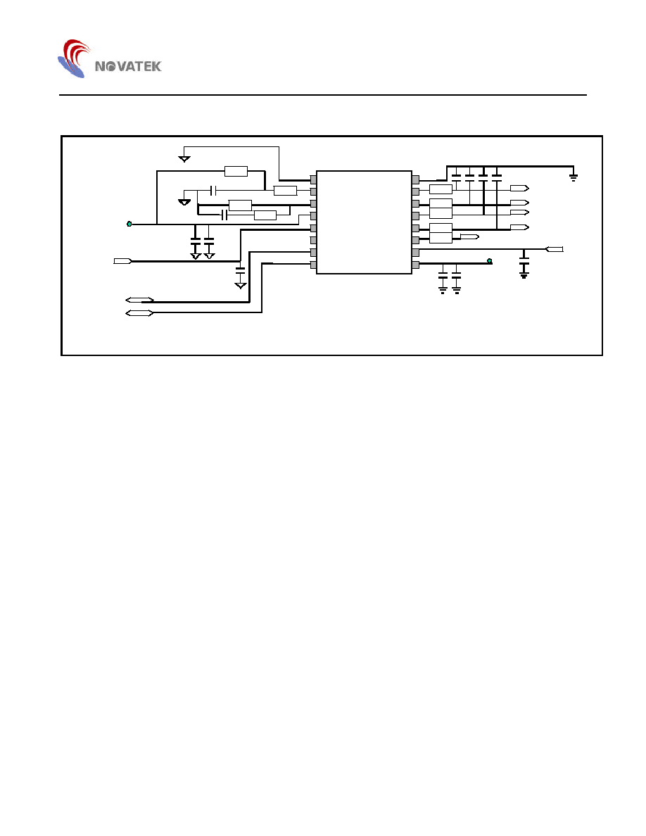
Application Circuit
V c c
5.6 K
12 K
1M
0.01uf
. .
.
.
.
0.01uf
5.6K
.
.
0.1u f
V c c
R
G
B
F B K G
PWMCLK/INT
V F L B
HFLB
SCL
S D A
16
15
14
13
12
11
10
9
1
2
3
4
5
6
7
8
AGND
VCO
R P
AVCC
HFLB
N C
SDA
SCL
DGND
R
G
B
FBKG
PWM/
/INT
VFLB
DVCC
220u f
100 p f
100 p f
470
470
470
470
220
100 p f
. .
. .
. . . .
.
. .
.
NT68275 Application Circuit
220 uf
0.1 uf
NT68275
38
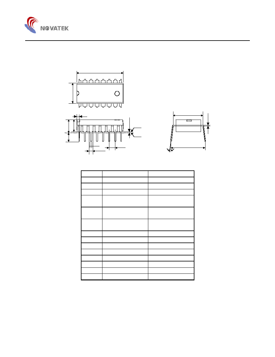
Package Information
P-DIP 16L Outline Dimensions
unit: inches/mm
1
8
16
D
E
1
S
A
2
A
L
C
E
e
A
9
B
1
B
e
1
Base Plane
A
1
Seating Plane
Symbol
Dimension in inch
Dimension in mm
A
0.175 Max.
4.45 Max.
A
1
0.010 Min.
0.25 Min.
A
2
0.130±0.010
3.30±0.25
B
0.018 +0.004
0.46 +0.10
-0.002
-0.05
B
1
0.060 +0.004
1.52 +0.10
-0.002
-0.05
C
0.010 +0.004
0.25 +0.10
-0.002
-0.05
D
0.750 Typ. (0.770 Max.) 19.05 Typ. (19.56 Max.)
E
0.300±0.010
7.62±0.25
E
1
0.250 Typ. (0.262 Max.)
6.35 Typ. (6.65 Max.)
e
1
0.100±0.010
2.54±0.25
L
0.130±0.010
3.30±0.25
0∞~ 15∞
0∞~ 15∞
e
A
0.345±0.035
8.76±0.89
S
0.040 Max.
1.02 Max.
Note:
1. The maximum value of dimension D includes end flash.
2. Dimension E1 does not include resin fins.
3. Dimension S includes end fl ash.