NT7502
65 X 132 RAM-Map LCD Controller / Driver
Features
!
Direct RAM data display using the display RAM. When
RAM data bit is 0, it is not displayed. When RAM data bit
is 1, it is displayed. (At normal display)
!
RAM capacity: 65 X 132 = 8580 bits
!
Many command functions: Read/Write Display Data.
Display ON/OFF. Normal/Reverse Display. Page
Address Set. Set Display Start Line. Set LCD Bias,
Electronic contrast Controls, V0 voltage regulation
internal resistor ratio set, Read Modify Write, Select
Segment Driver Direction, Power Save
!
High-speed 8-bit microprocessor interface allowing direct
connection to both the 8080 and 6800
!
Serial interface
!
Power supply voltage: 2.4 - 3.5V
!
Maximum 12V LCD driving output voltage
!
2X / 3X / 4X on chip DC-DC converter
!
Voltage regulator
!
Voltage follower
!
On-chip oscillator
General Description
The NT7502 is a single-chip LCD driver for dot-matrix liquid
crystal displays which is directly connectable to a
microcomputer bus. It accepts 8-bit serial or parallel display
data directly sent from a microcomputer and stores it in an
on-chip display RAM. It generates a LCD drive signal
independent of the microprocessor clock.
The set of the on-chip display RAM of 65 X 132 bits and a
one-to-one correspondence between LCD panel pixel dots
and on-chip RAM bits permit implementation of displays with
a high degree of freedom.
The NT7502 contains 65 common output circuits and 132
segment output circuits, so that a single chip of NT7502 can
make 65 X 132, 55 X 132, 49 X 132 and 33 X 132 dot
displays with pad option (DUTY1, DUTY0).
No external operation clock is required for RAM read/write
operations. Accordingly, this driver can be operated with a
minimum current consumption and its onboard
low-current-consumption liquid crystal power supply can
implement a high-performance handy display system with
minimum current consumption and the smallest LSI
configuration.
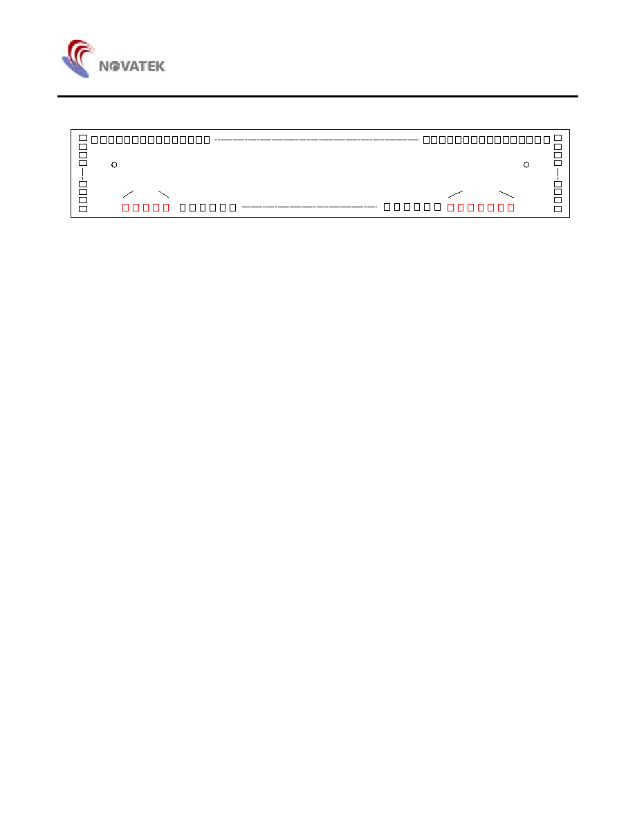
Pin Configuration
NT7502H-TABF1
(Copper Side View)
V4
CS
1
CS
2
RE
S
A0
WR
RD
D0
D1
D2
D3
D4
D5
D6
D7
DUTY
0
DUTY
1
VD
D
V
DD2
VSS
VOU
T
NC
C
AP3
+
C
AP1
-
C
AP2
+
C
AP2
-
VEXT
VR
S
V1
V2
V3
NC
V0
VR
M/
S
CLS
C86
P/
S
HP
M
NC
NC
NC
NC
FR
CL
DO
F
NC
IRS
C
AP1
+
40
41
42
43
44
45
46
1
2
3
4
5
6
7
8
9
10
11
12
13
14
15
16
17
18
19
20
21
22
23
24
25
26
27
28
29
30
31
32
33
34
35
36
37
38
39
47
243
244
245
246
247
CO
M
6
2
CO
M
6
3
CO
M
S
FRS
FR
211
212
213
214
215
SEG1
3
0
SEG1
3
1
CO
M
3
2
CO
M
3
3
CO
M
3
4
78
79
80
81
82
83
CO
M
1
CO
M
0
CO
M
S
SEG0
SEG1
SEG2
49
50
51
48
CO
M
3
1
CO
M
3
0
CO
M
2
9
CO
M
2
8
1
V1.0
NT7502
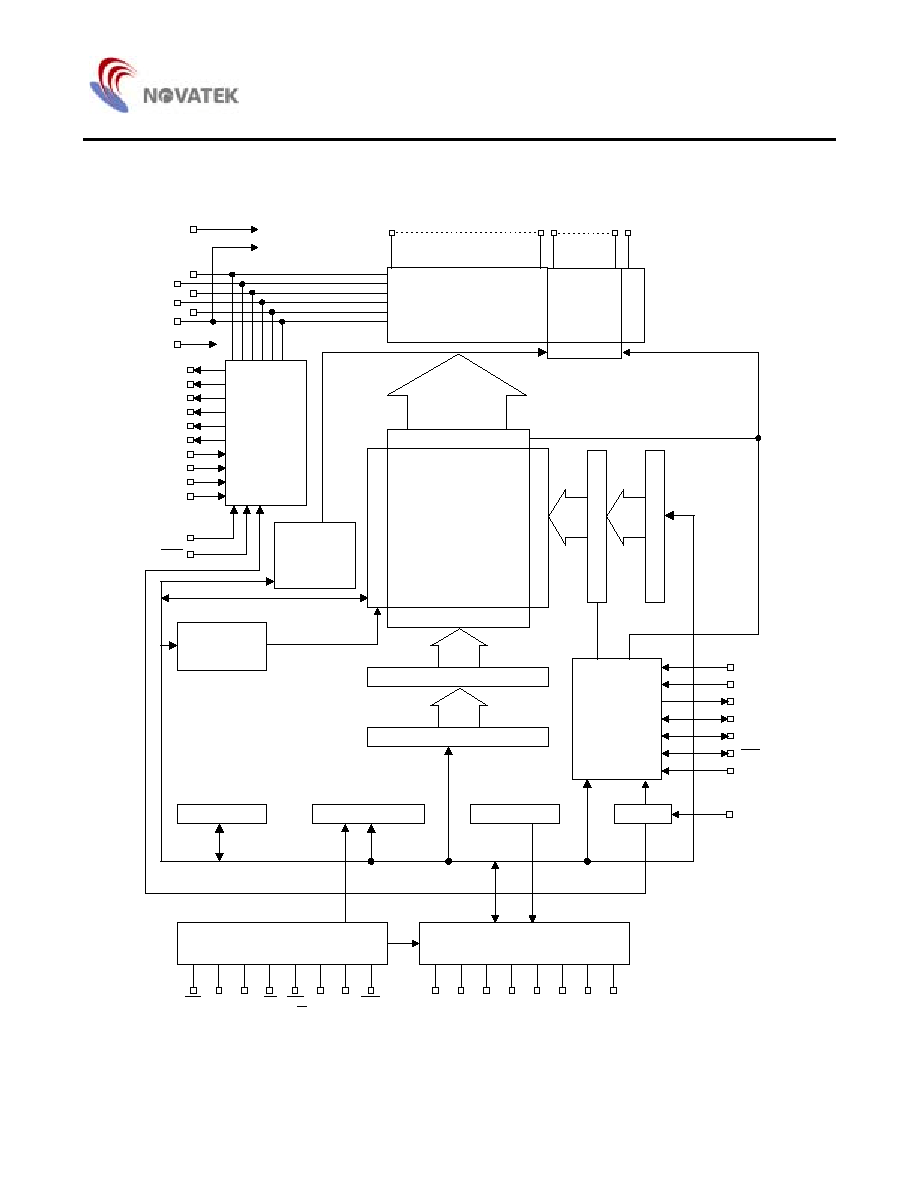
Block Diagram
Segment driver
Common
driver
Shift register
COM S
Power Supply
Circuit
Display data latch
132*65-dot
display data RAM
line address decoder
I/O buffer circuit
Line counter
Initial display line register
Output
status
selector
circuit
Column address decoder
8-bit column address counter
8-bit column address counter
Page address
register
Display timing
generator
circuit
Bus holder
Command decoder
Bus holder
Oscillator
Microprocessor interface
I/O buffer
SEG0
SEG131 COM0 COM63 COMS
V
0
V2
V4
V1
V3
Vss
CAP1+
CAP1-
CAP2+
CAP2-
CAP3+
V
OUT
CLS
CS2
A0
RD
(E)
WR
)
W
/
R
(
C86
P/S RES
1
CS
V
DD
D7
(SI)
D5
D4
D3
D2
D1
D0
D6
(SCL)
TMPS
V
DD2
V
R
V
RS
IRS
HPM
V
EXT
FRS
FR
CL
DOF
M/S
DUTY0
DUTY1
3
NT7502
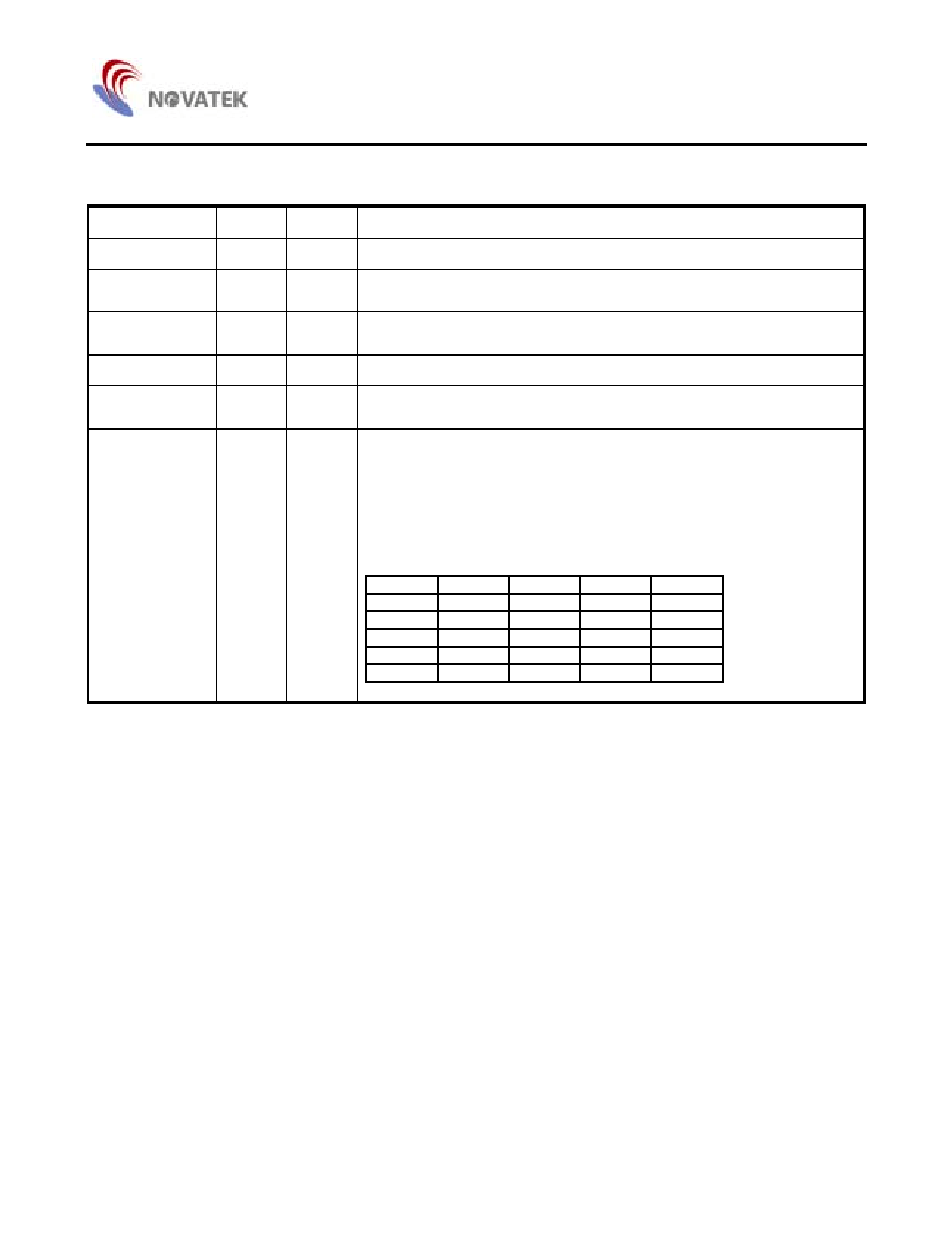
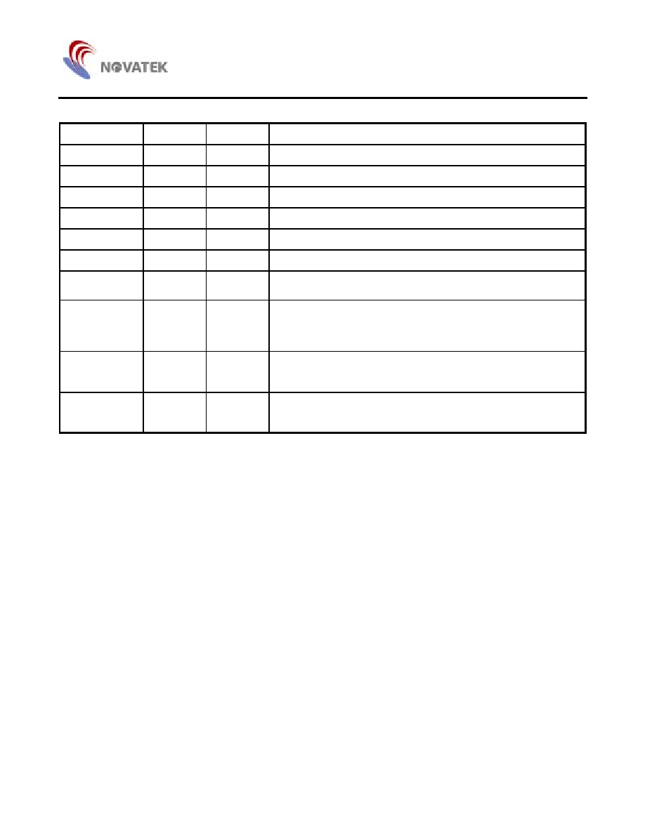
Pad Description
Power Supply
Pad No.
Symbol
I/O
Descriptions
30 - 33
V
DD
Supply
2.4 - 3.5V power supply input. These pads must be connected each other
10, 16, 26, 53, 71,
77, 81, 91
V
DD
Supply
2.4 - 3.5V power supply output for pad option
34 - 36
V
DD2
Supply
This is the reference power supply for the step-up voltage circuit for the LCD.
These pads must be connected each other
37 - 40
V
SS
Supply
Ground. These pads must be connected each other
7, 13, 25, 29 , 56,
69 - 70, 74, 79, 83
V
SS
Supply
Ground output for pad option
65 - 66
57 - 58
59 - 60
61 - 62
63 - 64
V
0
V
1
V
2
V
3
V
4
Supply
LCD driver supply voltages. The voltage determined by LCD cell is
impedance-converted by a resistive driver or an operation amplifier for
application. Voltages should be according to the following relationship:
V
0
V
1
V
2
V
3
V
4
V
SS
When the on-chip operating power circuit is on, the following voltages
are supplied to V
1
to V
4
by the on-chip power circuit. Voltage selection is
performed by the Set LCD Bias command.
LCD bias
V1
V2
V3
V4
1/5 bias
4/5V0
3/5V0
2/5V0
1/5V0
1/6 bias
5/6V0
4/6V0
2/6V0
1/6V0
1/7 bias
6/7V0
5/7V0
2/7V0
1/7V0
1/8 bias
7/8V0
6/8V0
2/8V0
1/8V0
1/9 bias
8/9V0
7/9V0
2/9V0
1/9V0
4
NT7502
LCD Driver Supplies
Pad No.
Symbol
I/O
Descriptions
45 - 46
CAP1-
O
Capacitor 1- pad for internal DC/DC voltage converter
47 - 48
CAP1+
O
Capacitor 1+ pad for internal DC/DC voltage converter
51 - 52
CAP2-
O
Capacitor 2- pad for internal DC/DC voltage converter
49 - 50
CAP2+
O
Capacitor 2+ pad for internal DC/DC voltage converter
43 - 44
CAP3+
O
Capacitor 3+ pad for internal DC/DC voltage converter
41 - 42
V
OUT
O
DC/DC voltage converter output
67 - 68
V
R
I
Voltage adjustment pad. Applies voltage between V
0
and V
SS
using a
resistive divider
54 V
EXT
I
This is the external input reference voltage (V
REF
) for the internal
voltage regulator. It is valid only when external V
REF
is used.
V
EXT
must be
2.4V and
V
DD2
When using internal V
REF
, this pad must be NC
82 TMPS
I
Selects temperature coefficient of the reference voltage
TMPS = 0: -0.05% /
∞
C
TMPS = 1: -0.2 % /
∞
C
55 VRS
I
Select the internal voltage regulator or external voltage regulator,
VRS = 0: using the external V
REF
VRS = 1: using the internal V
REF
5