
NT7706
240 Output LCD Segment/Common Driver
1/34
Ver2.0
Features
(Segment mode)
Shift Clock frequency:
20 MHz (Max.) (V
DD
= 5 V
10%)
Adopts a data bus system
4-bit/8-bit parallel input modes are selectable with a
mode (MD) pin
Automatic transfer function with an enable signal
Automatic counting function when in the chip select
mode, causes the internal clock to be stopped by
automatically counting 240 bits of input data
(Common mode)
Shift clock frequency :
4.0 MHz (Max.)
Built-in 240-bits bidirectional shift register (divisible into
120-bits x 2)
Available in a single mode (240-bits shift register) or in a
dual mode(120-bits shift register x 2)
1. Y1
Y240
Single mode
2. Y240
Y1
Single mode
3. Y1
Y120, Y121
Y240
Dual mode
4. Y240
Y121, Y120
Y1
Dual mode
The above 4 shift directions are pin-selectable
(Both for segment mode and common mode)
Supply voltage for LCD driver: 15.0 to 40.0 V
Number of LCD driver outputs: 240
Low output impedance
Low power consumption
Supply voltage for the logic system: +2.5 to +5.5 V
CMOS process
Package: Gold bump die
Not designed or rated as radiation hardened
General Description
The NT7706 is a 240-bit output segment/common driver LSI
suitable for driving large scale dot matrix LCD panels using
as PDA/personal computers/work stations. Through the use
of COG technology, it is ideal for substantially decreasing the
size of the frame section of the LCD module. The NT7706 is
good as both a segment driver and as a common driver, and
a low power consuming, high-precision LCD panel display
can be assembled using the NT7706. In the segment mode,
the data input is selected as 4bit parallel input mode or as
8bit parallel input mode by a mode (MD) pin. In the common
mode, the data input/output pins are bi-directional and the
four data shift directions are pin-selectable.

NT7706
2/34
Ver2.0
Pad Configuration
312
326
ALK_L
ALK_R
NT7706
x
x
1
80
81
95
96
311
x
Dummy Pad
Block Diagram
240 Bits 4 Level Driver
240 Bits Level Shifter
240 Bits Line Latch/Shift Register
Y1
Y2
Y239 Y240
V
43R
V
12R
V
0R
Level
Shifter
FR
DISPOFF
Active
Control
EIO
1
EIO
2
Control
Logic
SP Conversion & Data Control
(4 to 8 or 8 to 8)
D
0
D
1
D
2
D
3
D
4
D
5
D
6
D
7
L/R
MD
S/C
8Bitsx2
Data Latch
Data Latch Control
/8
/240
/240
V
DD
V
SS
V
SS
/16
/16
/16
/16
/16
LP
XCK
V
5R
V
5L
V
12L
V
0L
V
43L

NT7706
3/34
Ver2.0
Pad Description
Pad No.
Designation
I/O
Description
1-2, 324-326
V
0L
P
Power supply for LCD driver
3-5
V
12L
P
Power supply for LCD driver
6-8
V
43L
P
Power supply for LCD driver
9-10
V
5L
P
Power supply for LCD driver
11-16, 65-70
V
SS
P
Ground (0V), these pads must be connected to each other
17-22
V
DD
P
Power supply for the logic system (+2.5 to +5.5V)
23-24
S/C
I
Segment mode/common mode selection
25-26
EIO
2
I/O
Input/output for chip select or data of the shift register
27-47
D0 - D6
I
Display data input for segment mode
48-50
D7
I
Display data input for Segment mode/ Dual mode data input
51-52
XCK
I
Display data shift clock input for segment mode
53-54
DISPOFF
I
Control input for deselect output level
55-56
LP
I
Latch pulse input/shift clock input for the shift register
57-58
EIO
1
I/O
Input/output for chip select or data of the shift register
59-60
FR
I
AC-converting signal input for LCD driver waveform
61-62
L/R
I
Display data shift direction selection
63-64
MD
I
Mode selection input
71-72
V
5R
P
Power supply for LCD driver
73-75
V
43R
P
Power supply for LCD driver
76-78
V
12R
P
Power supply for LCD driver
79-83
V
0R
P
Power supply for LCD driver
84-323
Y1 - Y240
O
LCD driver output
NT7706
4/34
Ver2.0
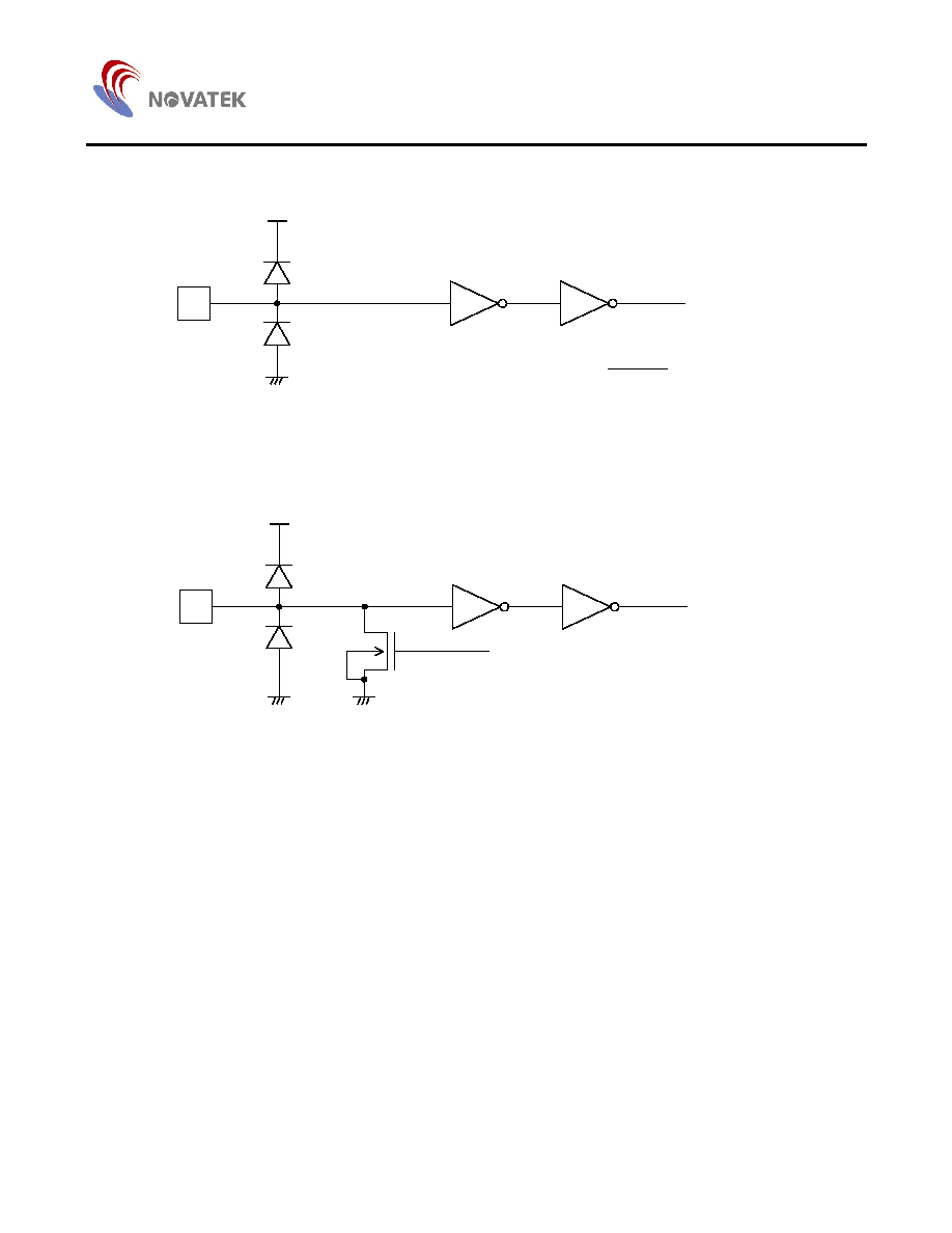
Input / Output Circuits
V
DD
V
SS
I
Input Signal
Applicable Pins
L/R, S/C, D0 - D6,
, LP, FR, MD
DISPOFF
Input Circuit (1)
V
DD
I
V
SS
V
SS
Input Signal
Control Signal
Applicable Pins
D7, XCK
Input Circuit (2)
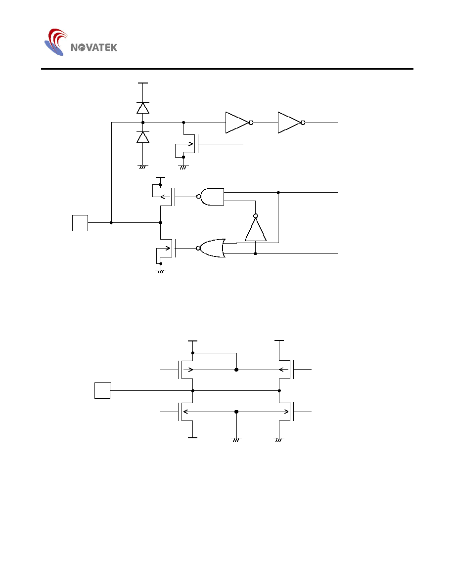
NT7706
5/34
Ver2.0
V
DD
I/O
V
SS
V
SS
Input Signal
Control Signal
Applicable Pins
EIO1, EIO2
Output Signal
Control Signal
V
SS
V
DD
Input / Output Circuit
Control Signal 1
Control Signal 3
Control Signal 2
Control Signal 4
V0
V12
O
V43
Applicable Pins
Y1 to Y240
V5
V
SS
LCD Driver Output circuit