
CF5005B series
NIPPON PRECISION CIRCUITS INC.--1
High-frequency Crystal Oscillator Module ICs
OVERVIEW
The CF5005B series are high-frequency crystal oscillator module ICs. They are comprised of an oscillator cir-
cuit and output buffer optimized for operation at 125 to 165MHz. The crystal oscillator circuit has a built-in
thin-film feedback resistor with good temperature characteristics and built-in capacitors with excellent fre-
quency response, making possible a stable 3rd-harmonic oscillator with only the addition of a crystal element.
FEATURES
I
3.0 to 3.6V operating supply voltage range
I
125 to 165MHz recommended operating fre-
quency range
I
Inverter amplifier feedback resistor built-in
I
Oscillator capacitors C
G
, C
D
built-in
I
Output three-state function (high impedance in
standby mode, oscillator stops)
I
f
O
output frequency (oscillator frequency)
I
8mA output drive capability (V
DD
= 3.0V)
I
CMOS output duty level
I
Chip form (CF5005B
��
)
SERIES CONFIGURATION
ORDERING INFORMATION
Version
Recommended
operating
frequency
1
[MHz]
1. The recommended operating frequency is a yardstick value derived from the crystal used for NPC characteristics authentication. However, the
oscillator frequency band is not guaranteed. Specifically, when used at high frequencies, the characteristics can vary greatly due to crystal char-
acteristics and mounting conditions, so the oscillation characteristics of components must be carefully evaluated.
gm ratio
Built-in capacitance [pF]
R
f
[k
]
C
G
C
D
CF5005BLA
125 to 150
1.0
1
6
2.2
CF5005BLB
140 to 165
1.0
1
3
2.2
Device
Package
CF5005B
��
�1
Chip form
CF5005B series
NIPPON PRECISION CIRCUITS INC.--2
PAD LAYOUT
(Unit:
�
m)
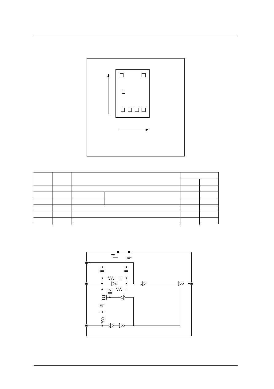
PIN DESCRIPTION and PAD DIMENSIONS
BLOCK DIAGRAM
Chip size: 0.92
�
1.31 mm
Chip thickness: 300 � 30 �m
Chip base: V
DD
level
Name
I/O
Description
Pad dimensions [�m]
X
Y
INHN
I
Output state control input. Oscillator stops when LOW. Pull-up resistor built in
195
212
XT
I
Amplifier input.
Crystal oscillator connection pins.
Crystal oscillator connected between XT and XTN
385
212
XTN
O
Amplifier output.
575
212
VSS
�
Ground
766
212
Q
O
Output. Output frequency (f
O
). High impedance in standby mode
765
1152
VDD
�
Supply voltage
162
1152
Substrate potential: V
DD
Q
VDD
XT
VSS
(0,0)
(920,1310)
X
Y
INHN
XTN
HA5005BL
XT
VSS
VDD
Q
C
G
C
D
R
f 1
XTN
INHN
R
f 2
C
f

CF5005B series
NIPPON PRECISION CIRCUITS INC.--3
SPECIFICATIONS
Absolute Maximum Ratings
V
SS
= 0V
Recommended Operating Conditions
V
SS
= 0V, f
165MHz, C
L
15pF unless otherwise noted.
Electrical Characteristics
V
DD
= 3.0 to 3.6V, V
SS
= 0V, Ta =
-
20 to 80
�
C unless otherwise noted.
Parameter
Symbol
Condition
Rating
Unit
Supply voltage range
V
DD
-
0.5 to 7.0
V
Input voltage range
V
IN
-
0.5 to V
DD
+ 0.5
V
Output voltage range
V
OUT
-
0.5 to V
DD
+ 0.5
V
Operating temperature range
T
opr
-
40 to 85
�
C
Storage temperature range
T
stg
-
65 to 150
�
C
Output current
I
OUT
25
mA
Parameter
Symbol
Condition
Rating
Unit
min
typ
max
Operating supply voltage
V
DD
3.0
�
3.6
V
Input voltage
V
IN
V
SS
�
V
DD
V
Operating temperature
T
OPR
-
20
�
80
�
C
Parameter
Symbol
Condition
Rating
Unit
min
typ
max
HIGH-level output voltage
V
OH
Q: Measurement cct 1, V
DD
= 3.0V, I
OH
= 8mA
2.5
2.7
�
V
LOW-level output voltage
V
OL
Q: Measurement cct 2, V
DD
= 3.0V, I
OL
= 8mA
�
0.3
0.4
V
Output leakage current
I
Z
Q: Measurement cct 2, INHN = LOW,
V
DD
= 3.6V
V
OH
= V
DD
�
�
10
�A
V
OL
= V
SS
�
�
10
HIGH-level input voltage
V
IH
INHN
0.7V
DD
�
�
V
LOW-level input voltage
V
IL
INHN
�
�
0.3V
DD
V
Current consumption
I
DD
Measurement cct 3, load cct 1,
INHN = open, C
L
= 15pF
f = 133MHz
�
30
65
mA
f = 156MHz
�
35
80
Standby current
I
ST
Measurement cct 3, INHN = LOW
�
�
10
�A
INHN pull-up resistance
R
UP1
Measurement cct 4
INHN = V
SS
0.4
�
4
M
R
UP2
INHN = 0.7V
DD
50
�
150
k
AC feedback resistance
R
f1
Design value, determined by the internal wafer pattern
1.76
2.2
2.64
k
DC feedback resistance
R
f2
Measurement cct 5
50
�
150
k
AC feedback capacitance
C
f
Design value, determined by the internal wafer pattern
9.3
10
10.7
pF
Built-in capacitance
C
G
Design value, determined by the
internal wafer pattern
CF5005BLA
0.93
1
1.07
pF
CF5005BLB
0.93
1
1.07
C
D
Design value, determined by the
internal wafer pattern
CF5005BLA
5.58
6
6.42
pF
CF5005BLB
2.79
3
3.21

CF5005B series
NIPPON PRECISION CIRCUITS INC.--4
Switching Characteristics
V
DD
= 3.0 to 3.6V, V
SS
= 0V, Ta =
-
20 to 80
�
C unless otherwise noted.
FUNCTIONAL DESCRIPTION
Standby Function
The oscillator stops when INHN goes LOW. When the oscillator stops, the oscillator output on Q goes high
impedance.
Parameter
Symbol
Condition
Rating
Unit
min
typ
max
Output rise time
t
r
Measurement cct 3, load cct 1, 0.1V
DD
to 0.9V
DD
, C
L
= 15pF
�
1.5
2.5
ns
Output fall time
t
f
Measurement cct 3, load cct 1, 0.9V
DD
to 0.1V
DD
, C
L
= 15pF
�
1.5
2.5
ns
Output duty cycle
1
1. Monitored in sample lots.
Duty
Measurement cct 3, load cct 1, Ta = 25
�
C, V
DD
= 3.3V, C
L
= 15pF,
f
165MHz
40
�
60
%
Output disable delay time
2
2. Oscillator stop function is built-in. When INHN goes LOW, normal output stops. When INHN goes HIGH, normal output is not resumed until after the
oscillator start-up time has elapsed.
t
PLZ
Measurement cct 6, load cct 1, Ta = 25
�
C, V
DD
= 3.0V, C
L
15pF
�
�
100
ns
Output enable delay time
2
t
PZL
Measurement cct 6, load cct 1, Ta = 25
�
C, V
DD
= 3.0V, C
L
15pF
�
�
100
ns
INHN
Q
Oscillator
HIGH (or open)
f
O
output frequency
Normal operation
LOW
High impedance
Stopped

CF5005B series
NIPPON PRECISION CIRCUITS INC.--5
MEASUREMENT CIRCUITS
Measurement cct 1
2.5V
P
-
P
, 10MHz sine wave input signal
C1 : 0.001
�
F
R1 : 50
R2 : 312.5
Measurement cct 4
Measurement cct 2
Measurement cct 5
Measurement cct 3
Measurement cct 6
R1 : 50
Signal
Generator
VDD
VSS
XT
Q
R1
R2
C1
V
OH
0V
Q output
VDD
VSS
I
PR
INHN
V
PR
R
UP1
=
V
DD
I
PR
(V
PR
= V
SS
)
R
UP2
=
I
PR
(V
PR
= 0.7V
DD
)
V
DD
0.7V
DD
A
V
VDD
VSS
Q
V
OL
V
A
I
OL
, I
Z
I
Z
INHN
VDD
VSS
I
Rf
R
f2
=
XT
V
DD
I
Rf
XTN
A
VDD
VSS
XT
Q
X'tal
XTN
INHN
I
DD
I
ST
A
Signal
Generator
VSS
XT
Q
R1
VDD
INHN