
SM5007 series
NIPPON PRECISION CIRCUITS--1
NIPPON PRECISION CIRCUITS INC.
Crystal Oscillator Module ICs
OVERVIEW
The SM5007 series are crystal oscillator module ICs, that feature low current consumption. Highly accurate
thin-film feedback resistors and high-frequency capacitors are built-in, eliminating the need for external com-
ponents to make a stable fundamental-harmonic oscillator.
FEATURES
I
Capacitors C
G
, C
D
built-in
I
Standby function (oscillator stops)
I
6 µA (typ.) low standby current (5 V operation)
I
Power-save pull-up resistor built-in
I
Inverter amplifier feedback resistor built-in
I
3.2 mA (V
DD
= 4.5 V), 1.6 mA (V
DD
= 2.7 V)
drive capability
I
2.7 to 5.5 V supply voltage
I
Low current consumption
I
Oscillator frequency output
(f
O
or f
O
/2, determined by internal connection)
I
8-pin VSOP (SM5007AL
◊
V)
I
Chip form (CF5007A
◊◊
)
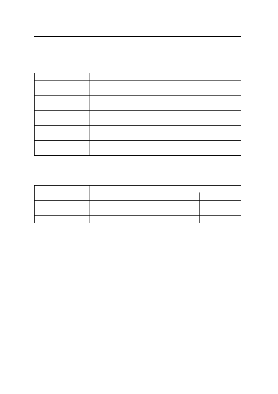
SERIES CONFIGURATION
Note: R e c o m m e n d e d o p e r ating frequency is not the guaranteed value but is measured using NPC's standard crystal.
Since the product feature is targeted at low current consumption, please evaluate oscillation margins seriously before actual use.
ORDERING INFORMATION
V ersion
R e c o m m e n d e d
Operating
frequency [MHz]
Output
frequency
gm ratio
Built-in capacitance
[pF]
Input level
Output duty
level
S t a n d by
output state
3 V
5 V
C
G
C
D
C F 5 0 0 7 A A 1
3 0
3 0
f
O
2
1 0
1 0
T T L
C M O S
L O W
C F 5 0 0 7 A A 2
3 0
3 0
f
O
/2
2
1 0
1 0
T T L
C M O S
L O W
S M 5 0 0 7 A L 1 V
C F 5 0 0 7 A L 1
2 0
3 0
f
O
1
1 0
1 0
C M O S
C M O S
High
i m p e d a n c e
S M 5 0 0 7 A L 2 V
C F 5 0 0 7 A L 2
2 0
3 0
f
O
/2
1
1 0
1 0
C M O S
C M O S
High
i m p e d a n c e
D e vice
P a ck ag e
S M 5 0 0 7 A L
◊
V
8-pin V S O P
C F 5 0 0 7 A
◊◊
≠ 1
Chip form

SM5007 series
NIPPON PRECISION CIRCUITS--2
PACKAGE DIMENSIONS
(Unit : mm)
∑ 8-pin VSOP
4.4 0.2
6.4 0.3
3.1 0.3
0.22 0.1
1.15 0.05
0.5 0.2
0.575typ
0.15
+ 0.1
- 0.05
0.12
0.10
0.1 0.05
0.65
M
0 to 10

SM5007 series
NIPPON PRECISION CIRCUITS--3
PAD LAYOUT
(Unit :
µ
m)
PINOUT
(Top view)
PIN DESCRIPTION and PAD DIMENSIONS
BLOCK DIAGRAM
Chip size: 0.92
◊
1.04 mm
Chip thickness: 300 ± 30 µm
Chip base: V
D D
level
Q
VDD
XT
VSS
(0,0)
(920,1040)
X
Y
HA5007
INH
XT
1
XT
VSS
Q
VDD
NC
NC
0 0 7
XT
INH
2
3
4
8
7
6
5
N u m b e r
N a m e
I/O
Description
P ad dimensions [µm]
X
Y
1
I N H
I
Output state control input. Oscillator stopped when LOW . Pow er-saving pull-up
resistor built in
1 9 5
2 1 2
2
X T
I
Amplifier input.
Cr ystal oscillator connection pins.
Cr ystal oscillator connected between XT and X T
3 8 5
2 1 2
3
X T
O
Amplifier output.
5 7 5
2 1 2
4
V S S
≠
G r o u n d
7 6 6
2 1 2
5
Q
O
Output. Output frequency (f
O
or f
O
/2) determined by internal connection
7 6 5
8 8 2
6
N C
≠
No connection
≠
≠
7
N C
≠
No connection
≠
≠
8
V D D
≠
Supply voltage
1 6 2
8 8 2
XT
VSS
VDD
Q
C
G
C
D
1/2
R
f
XT
INH
SM5007 series
NIPPON PRECISION CIRCUITS--4
SPECIFICATIONS
Absolute Maximum Ratings
V
SS
= 0 V
Recommended Operating Conditions
V
SS
= 0 V
Note: Since the recommended operating conditions will change in accordance with operating frequency, load capacitance, pow er dissipation, or crystal
characteristics, please evaluate oscillation margins seriously before actual use.
P arameter
S y m b o l
Condition
Rating
Unit
Supply voltage ra n g e
V
D D
-
0.5 to 7.0
V
Input voltage ra n g e
V
IN
-
0.5 to V
D D
+ 0.5
V
Output voltage ra n g e
V
O U T
-
0.5 to V
D D
+ 0.5
V
O p e rating temperature ra n g e
T
opr
-
40 to 85
∞
C
Storage temperature ra n g e
T
stg
Chip form
-
65 to 150
∞
C
8-pin V S O P
-
55 to 125
Output current
I
O U T
1 5
m A
P ow er dissipation
P
D
8-pin V S O P
3 0 0
m W
Soldering temperature
T
sld
8-pin V S O P
2 5 5
∞
C
Soldering time
t
sld
8-pin V S O P
1 0
s
P arameter
S y m b o l
Condition
Rating
Unit
m i n
typ
m a x
Supply voltage
V
D D
2.7
≠
5.5
V
Input voltage
V
IN
V
S S
≠
V
D D
V
O p e rating temperature
T
O P R
-
2 0
≠
8 0
∞
C

SM5007 series
NIPPON PRECISION CIRCUITS--5
Electrical Characteristics
3 V operation: V
DD
= 2.7 to 3.3 V, V
SS
= 0 V, Ta =
-
20 to 80
∞
C unless otherwise noted.
P arameter
S y m b o l
Condition
Rating
Unit
m i n
typ
m a x
HIGH-level output voltage
V
O H
Q: Measurement cct 1, I
O H
= 1.6 m A
2.2
≠
≠
V
L O W -level output voltage
V
O L
Q: Measurement cct 1, I
O L
= 1.6 m A
≠
≠
0.4
V
Output leakage current
(AL series only)
I
Z
Q: Measurement cct 2, I N H = L O W , V
O H
= V
D D
≠
≠
1 0
µ A
Q: Measurement cct 2, I N H = L O W , V
O L
= V
S S
≠
≠
1 0
HIGH-level input voltage
V
IH
I N H
S M 5 0 0 7 A L
◊
V
C F 5 0 0 7 A L
◊
0.7V
D D
≠
≠
V
C F 5 0 0 7 A A
◊
2.0
≠
≠
L O W -level input voltage
V
IL
I N H
S M 5 0 0 7 A L
◊
V
C F 5 0 0 7 A L
◊
≠
≠
0.3V
D D
V
C F 5 0 0 7 A A
◊
≠
≠
0.3
Current consumption
I
D D 1
I N H = open, Measurement cct 3, No load,
f = 30 MHz cr ystal oscillator
C F 5 0 0 7 A A 1
1.8
4.8
m A
S M 5 0 0 7 A L 1 V
C F 5 0 0 7 A L 1
1.2
3.2
C F 5 0 0 7 A A 2
1.4
3.6
S M 5 0 0 7 A L 2 V
C F 5 0 0 7 A L 2
0.8
2.0
I
D D 2
I N H = open, Measurement cct 3,
C
L
= 15 p F, f = 30 MHz cr ystal oscillator
C F 5 0 0 7 A A 1
3.4
6.8
S M 5 0 0 7 A L 1 V
C F 5 0 0 7 A L 1
2.8
5.2
C F 5 0 0 7 A A 2
2.2
4.6
S M 5 0 0 7 A L 2 V
C F 5 0 0 7 A L 2
1.6
3.0
Standby current
I
S T
I N H = V
S S
, Measurement cct 3
≠
2
5
µ A
I N H pull-up resistance
R
U P 1
Measurement cct 4, V
D D
= 3 V, I N H = V
S S
0.6
≠
1 2
M
R
U P 2
Measurement cct 4, V
D D
= 3 V, I N H = 2.1 V
4 0
≠
2 0 0
k
Negative resistance
-
R
L
V
D D
= 3 V, Ta = 25
∞
C , 30 M H z
C F 5 0 0 7 A A
◊
≠ 1 4 0
S M 5 0 0 7 A L
◊
V
C F 5 0 0 7 A L
◊
≠ 7 0
F e e d b a ck resistance
R
f
Measurement cct 5
5 0
≠
3 0 0
k
Built-in capacitance
C
G
Design value
9.3
1 0
10.7
p F
C
D
9.3
1 0
10.7
p F