
CF5012 series
NIPPON PRECISION CIRCUITS INC.--1
Low-current Consumption Crystal Oscillator Module ICs
OVERVIEW
The CF5012 series are low-current consumption 3rd-harmonic crystal oscillator module ICs. Internal circuit
optimization means these devices have reduced current consumption in comparison with our existing 3rd-har-
monic oscillator devices. The crystal oscillator circuit has a built-in thin-film feedback resistor with good tem-
perature characteristics and built-in capacitors with excellent frequency response, resulting in a stable 3rd-
order overtone oscillator with only the connection of a crystal element.
FEATURES
I
3rd-harmonic oscillation
I
2.7 to 3.6V operating supply voltage range
I
30 to 45MHz recommended operating frequency
range
I
Inverter amplifier feedback resistor built-in
I
Oscillator capacitors C
G
, C
D
built-in
I
Output three-state function
(high impedance in standby mode)
I
f
O
output frequency (oscillator frequency)
I
8mA output drive capability (V
DD
= 2.7V)
I
6.5mA (typ) low current consumption
(V
DD
= 3V, C
L
= 15pF, f = 40MHz)
I
CMOS output duty level
I
Chip form (CF5012
���
)
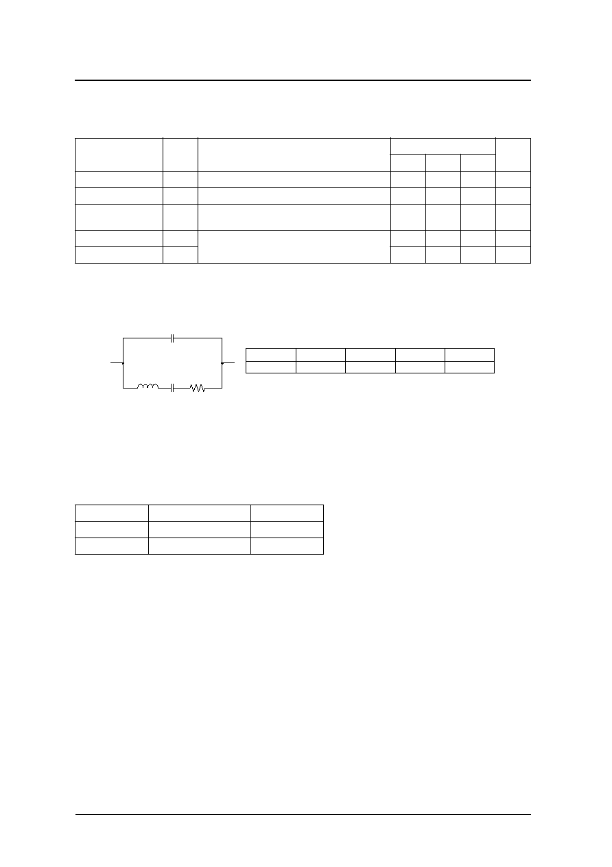
SERIES CONFIGURATION
Note: Recommended operating frequency is not the guaranteed value but is measured using NPC's standard crystal.
ORDERING INFORMATION
Version
Recommended
operating
frequency [MHz]
gm ratio
Built-in capacitance [pF]
R
f
[k
]
C
G
C
D
CF5012ANB
30 to 45
1.0
8
15
3.1
Device
Package
CF5012
���
�1
Chip form

CF5012 series
NIPPON PRECISION CIRCUITS INC.--2
PAD LAYOUT
(Unit:
�
m)
PIN DESCRIPTION and PAD DIMENSIONS
BLOCK DIAGRAM
Chip size: 0.92
�
1.18 mm
Chip thickness: 300 � 30 �m
Chip base: V
DD
level
Name
I/O
Description
Pad dimensions [�m]
X
Y
INHN
I
Output state control input. High impedance when LOW. Pull-up resistor built in
195
174.4
XT
I
Amplifier input
Crystal oscillator connection pins.
Crystal oscillator connected between XT and XTN
385
174.4
XTN
O
Amplifier output
575
174.4
VSS
�
Ground
765
174.4
Q
O
Output. Output frequency. High impedance in standby mode
757.6
1017.6
VDD
�
Supply voltage
165.4
1014.6
Substrate potential: V
DD
Q
VDD
XT
VSS
(0,0)
(920,1180)
X
Y
INHN
XTN
HA5012ANB
XT
VSS
VDD
Q
C
G
C
D
XTN
INHN
R
f

CF5012 series
NIPPON PRECISION CIRCUITS INC.--3
SPECIFICATIONS
Absolute Maximum Ratings
V
SS
= 0V
Recommended Operating Conditions
V
SS
= 0V, f
45MHz, C
L
= 15pF unless otherwise noted.
Electrical Characteristics
V
DD
= 2.7 to 3.6V, V
SS
= 0V, Ta =
-
20 to +80
�
C unless otherwise noted.
Parameter
Symbol
Condition
Rating
Unit
Supply voltage range
V
DD
-
0.5 to +7.0
V
Input voltage range
V
IN
-
0.5 to V
DD
+ 0.5
V
Output voltage range
V
OUT
-
0.5 to V
DD
+ 0.5
V
Operating temperature range
T
opr
-
40 to +85
�
C
Storage temperature range
T
stg
-
65 to +150
�
C
Output current
I
OUT
25
mA
Parameter
Symbol
Condition
Rating
Unit
min
typ
max
Supply voltage
V
DD
2.7
�
3.6
V
Input voltage
V
IN
V
SS
�
V
DD
V
Operating temperature
T
OPR
-
20
�
+80
�
C
Parameter
Symbol
Condition
Rating
Unit
min
typ
max
HIGH-level output voltage
V
OH
Q: Measurement cct 1, V
DD
= 2.7V, I
OH
= 8mA
2.2
2.4
�
V
LOW-level output voltage
V
OL
Q: Measurement cct 2, V
DD
= 2.7V, I
OL
= 8mA
�
0.3
0.4
V
Output leakage current
I
Z
Q: Measurement cct 2, INHN = LOW,
V
DD
= 3.6V
V
OH
= V
DD
�
�
10
�A
V
OL
= V
SS
�
�
10
�A
HIGH-level input voltage
V
IH
INHN
0.7V
DD
�
�
V
LOW-level input voltage
V
IL
INHN
�
�
0.3V
DD
V
Current consumption
I
DD
Measurement cct 3, load cct 1, INHN = open, C
L
= 15pF,
f = 40MHz
�
6.5
13
mA
INHN pull-up resistance
R
UP
Measurement cct 4
40
100
250
k
Feedback resistance
R
f
Measurement cct 5
2.63
3.1
3.57
k
Built-in capacitance
C
G
Design value, determined by the internal wafer pattern
7
8
9
pF
C
D
13
15
17
pF
CF5012 series
NIPPON PRECISION CIRCUITS INC.--4
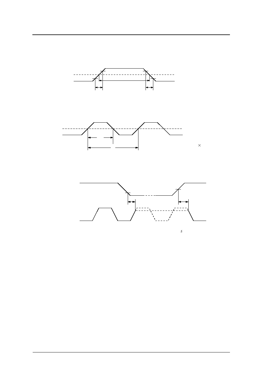
Switching Characteristics
V
DD
= 2.7 to 3.6V, V
SS
= 0V, Ta =
-
20 to +80
�
C unless otherwise noted.
Current consumption and Output waveform with NPC's standard crystal
FUNCTIONAL DESCRIPTION
Standby Function
When INHN goes LOW, the oscillator output on Q goes high impedance.
Parameter
Symbol
Condition
Rating
Unit
min
typ
max
Output rise time
t
r
Measurement cct 3, load cct 1, 0.1V
DD
to 0.9V
DD
, C
L
= 15pF
�
2.0
4.0
ns
Output fall time
t
f
Measurement cct 3, load cct 1, 0.9V
DD
to 0.1V
DD
, C
L
= 15pF
�
2.0
4.0
ns
Output duty cycle
1
1. Monitored in sample lots.
Duty
Measurement cct 3, load cct 1, Ta = 25
�
C, V
DD
= 3.0V,
C
L
= 15pF, f = 40MHz
40
�
60
%
Output disable delay time
t
PLZ
Measurement cct 3, load cct 1, Ta = 25
�
C, V
DD
= 3.0V,
C
L
= 15pF
�
�
100
ns
Output enable delay time
t
PZL
�
�
100
ns
INHN
Q
Oscillator
HIGH (or open)
f
O
output frequency
Normal operation
LOW
High impedance
Normal operation
f (MHz)
R (
)
L (mH)
Ca (fF)
Cb (pF)
40
20.53
11.34
1.396
3.989
L
Ca
R
Cb
CF5012 series
NIPPON PRECISION CIRCUITS INC.--5
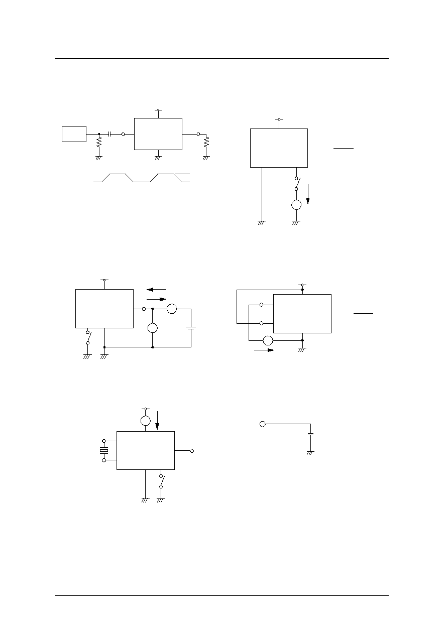
MEASUREMENT CIRCUITS
Measurement cct 1
2.0V
P
-
P
, 10MHz sine wave input signal
C1 : 0.001
�
F
R1 : 50
R2 : 275
Measurement cct 4
Measurement cct 2
Measurement cct 5
Measurement cct 3
Load cct 1
C
L
= 15pF
Signal
Generator
VDD
VSS
XT
Q
R1
R2
C1
V
OH
0V
Q output
VDD
VSS
I
PR
INHN
R
UP
=
V
DD
I
PR
A
VDD
VSS
Q
V
OL
V
A
I
OL
, I
Z
I
Z
INHN
VDD
VSS
I
Rf
R
f
=
XT
V
DD
I
Rf
XTN
A
VDD
VSS
XT
Q
X'tal
XTN
INHN
I
DD
A
Q output
C
L
(Including probe capacitance)
CF5012 series
NIPPON PRECISION CIRCUITS INC.--6
Switching Time Measurement Waveform
T
r
, T
f
, Duty
Output duty cycle
Output Enable/Disable Delay
0.9V
DD
0.1V
DD
0.9V
DD
0.1V
DD
t
r
t
f
Q output
DUTY measurement
voltage (0.5V
DD
)
T
W
DUTY measurement
voltage
(
0.5V
DD
)
Q output
T
W
T
DUTY= T
W
/ T 100 (%)
Q output
INHN
V
IH
V
IL
t
PLZ
t
PZL
INHN input waveform
t
r =
t
f 10ns

CF5012 series
NIPPON PRECISION CIRCUITS INC.--7
NC0111AE
2002.01
NIPPON PRECISION CIRCUITS INC. reserves the right to make changes to the products described in this data sheet in order to
improve the design or performance and to supply the best possible products. Nippon Precision Circuits Inc. assumes no responsibility for
the use of any circuits shown in this data sheet, conveys no license under any patent or other rights, and makes no claim that the circuits
are free from patent infringement. Applications for any devices shown in this data sheet are for illustration only and Nippon Precision
Circuits Inc. makes no claim or warranty that such applications will be suitable for the use specified without further testing or modification.
The products described in this data sheet are not intended to use for the apparatus which influence human lives due to the failure or
malfunction of the products. Customers are requested to comply with applicable laws and regulations in effect now and hereinafter,
including compliance with export controls on the distribution or dissemination of the products. Customers shall not export, directly or
indirectly, any products without first obtaining required licenses and approvals from appropriate government agencies.
NIPPON PRECISION CIRCUITS INC.
4-3, Fukuzumi 2-chome, Koto-ku,
Tokyo 135-8430, Japan
Telephone: +81-3-3642-6661
Facsimile: +81-3-3642-6698
http://www.npc.co.jp/
Email: sales
@
npc.co.jp