
SM5050A
NIPPON PRECISION CIRCUITS--1
NIPPON PRECISION CIRCUITS INC.
Single-output Clock Generator IC
OVERVIEW
The SM5050A is a single-output clock generator IC that generates standard high-frequency clocks derived
from a 20 to 40MHz crystal oscillator master clock. The high-frequency output stage uses optimized PLL cir-
cuits for low jitter output. The oscillator capacitors C
G
and C
D
are built-in, realizing a high-frequency output
oscillator by just the connection of a crystal. Two program inputs allows selection from 4 frequency multipli-
ers, making the SM5050A able to generate multi-standard frequency clock outputs.
FEATURES
s
2.7 to 3.6V operating supply voltage
s
20 to 40MHz master clock frequency (fundamen-
tal)
s
Output frequency ranges
� 100 to 166.6MHz (V
DD
= V
DDQ
= 3.0 to 3.6V)
� 100 to 125MHz (V
DD
= V
DDQ
= 2.7 to 3.6V)
s
8mA output drive capability
s
Oscillator capacitors (C
G
, C
D
) and feedback resis-
tor (R
f
) built-in
s
100ps (typ) low jitter output (peak-to-peak)
s
2 program inputs for 4 selectable multiplier ratios
s
Standby function
s
Packaging
� Chip form (CF5050A)
� 8-pin VSOP package (SM5050AV)
PINOUT
ORDERING INFORMATION
PAD DIMENSIONS
PACKAGE DIMENSIONS
(Top view )
D e vice
P a ck ag e
C F 5 0 5 0 A � 1
Chip form
S M 5 0 5 0 A V
8-pin V S O P
1
P1
2
VSS
3
Q
4
VDD
5
XTN
6
XT
7
INHN
8
P0
(Unit: �m)
Chip size: 2.16
�
1 . 5 7 m m
Chip thickness: 300 � 30�m
Chip base: V
S S
level
(Unit: m m )
Q
VDD
XTN
VSS
(0,0)
(2160,1570)
INHN
XT
SA5050A
VDDQ
VSSQ
P1
P0
0.575 typ
3.1
�
0.3
1.15
� 0.05
4.4
� 0.2
6.4
�
0.3
0.5
� 0.2
0.1
� 0.05
0.22
� 0.1
0.65
0.12
M
0.10
0 to 10
0.15
+
0.1
-
0.05
S M 5 0 5 0 A
NIPPON PRECISION CIRCUITS--2
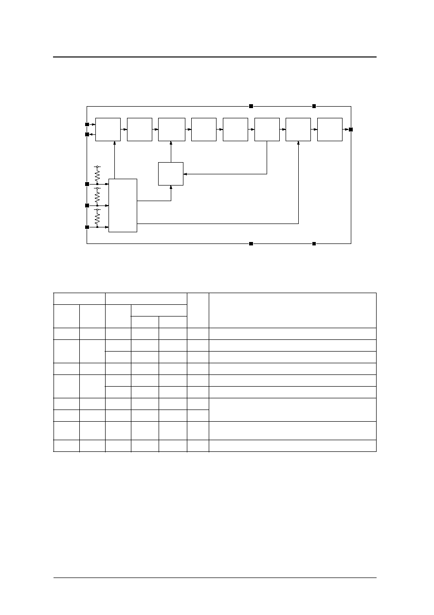
BLOCK DIAGRAM
PIN DESCRIPTION
S M 5 0 5 0 A V
C F 5 0 5 0 A
I/O
1
1. Ip = input with built-in pull-up resistor.
Description
N u m b e r
N a m e
N a m e
P ad dimensions [�m]
X
Y
1
P 1
P 1
6 2 0
1 3 3 0
Ip
Program input 1. Selects the output frequency multiplier ratio.
2
V S S
V S S
2 9 0
1 1 3 2
�
G r o u n d
V S S Q
2 9 0
9 2 0
�
Output circuit ground
3
Q
Q
2 9 0
5 6 9
O
Output (CMOS)
4
V D D
V D D Q
5 4 0
2 4 0
�
Output circuit supply
V D D
9 0 6
2 4 0
�
Supply
5
X T N
X T N
1 5 2 4
2 4 0
O
Cr ystal oscillator connection pins.
Cr ystal connected between XT and XTN.
6
X T
X T
1 8 7 0
5 4 2
I
7
I N H N
I N H N
1 8 7 0
1 0 1 5
Ip
O p e rating state control (inhibit).
When INHN is LOW , output is high impedance and PLL circuits stop.
8
P 0
P 0
1 5 4 0
1 3 3 0
Ip
Program input 0. Selects the output frequency multiplier ratio.
VCO
XT
XTN
LPF
Q
P0
P1
INHN
Phase
Detector
Charge
Pump
Oscillator
R-counter
Duty
Control
Circuit
Output
Buffer
N-counter
Control
Circuit
VDDQ
VDD
VSSQ
VSS

S M 5 0 5 0 A
NIPPON PRECISION CIRCUITS--3
OUTPUT FREQUENCY SETTINGS
Note: The output frequency range is 100 to 166.6MHz. The master clock frequency can be adjusted to any value within the range 20 to 40MHz,
so the master clock frequency and multiplier should be selected such that the output frequency is within the output frequency ra n g e.
SPECIFICATIONS
Absolute Maximum Ratings
V
SS
= 0V
Recommended Operating Conditions
V
SS
= 0V, f
OUT
= 100 to 166.6MHz, C
L
= 15pF
Program inputs
Multiplier ratio
Master clock
frequency [MHz]
Output frequency
[ M H z ]
S u p p ly voltag e [V]
P 0
P 1
L O W
L O W
�
4
25.00
1 0 0
2.7 to 3.6
L O W
H I G H
�
4.25
25.00
106.25
H I G H
L O W
�
5
25.00
1 2 5
26.66
133.3
3.0 to 3.6
H I G H
H I G H
�
6.25
24.8832
155.52
26.66
166.6
P arameter
S y m b o l
Condition
Rating
Unit
Supply voltage ra n g e
V
D D
-
0.5 to 6.0
V
Input voltage ra n g e
V
IN
-
0.5 to V
D D
+ 0.5
V
Output voltage ra n g e
V
O U T
-
0.5 to V
D D
+ 0.5
V
Storage temperature ra n g e
T
stg
C F 5 0 5 0 A
-
65 to 150
�
C
S M 5 0 5 0 A V
-
55 to 125
�
C
O p e rating temperature ra n g e
T
opr
-
40 to 85
�
C
Output current
I
O U T
2 5
m A
P ow er dissipation
P
D
S M 5 0 5 0 A V
1 5 0
m W
P arameter
S y m b o l
Condition
Rating
Unit
m i n
typ
m a x
O p e rating supply voltage
V
D D
f
O U T
1 2 5 M H z
2.7
�
3.6
V
f
O U T
1 6 6 . 6 M H z
3.0
�
3.6
Input voltage
V
IN
V
S S
�
V
D D
V
O p e rating temperature
T
opr
-
2 0
�
8 0
�
C

S M 5 0 5 0 A
NIPPON PRECISION CIRCUITS--4
DC Characteristics
V
DD
= 2.7 to 3.6V, V
SS
= 0V, Ta =
-
20 to 80
�
C unless otherwise noted
P arameter
S y m b o l
Condition
Rating
Unit
m i n
typ
m a x
Q HIGH-level output voltage
V
O H
V
D D
= 2.7V, I
O H
= 8mA
2.2
�
�
V
Q L OW -level output voltage
V
O L
V
D D
= 2.7V, I
O L
= 8mA
�
�
0.4
V
Q output leakage current
I
Z
Measurement circuit 4,
INHN = V
S S
V
O H
= V
D D
�
�
1 0
� A
V
O L
= V
S S
�
�
1 0
INHN HIGH-level input voltage
V
IH1
0.7V
D D
�
�
V
P0, P1 HIGH-level input voltage
V
IH2
0.9V
D D
�
�
V
I N H N L OW -level input voltage
V
IL1
�
�
0.3V
D D
V
P0, P1 LOW -level input voltage
V
IL2
�
�
0.1V
D D
V
Current consumption
I
D D
25MHz cr ystal, measurement circuit 1,
load circuit 1, INHN = open, C
L
= 15pF,
P0 = HIGH, P1 = LOW , V
D D
= 3.0V
�
2 3
�
m A
25MHz cr ystal, measurement circuit 1,
load circuit 1, INHN = open, C
L
= 15pF,
P0 = HIGH, P1 = LOW
�
�
4 2
Standby current
I
S T
INHN = V
S S
, measurement circuit 1
�
�
4 0
� A
INHN, P0, P1 input pull-up
resistance
R
U P 1
V
D D
= 3V, measurement circuit 2
0.3
�
6
M
R
U P 2
1 0
�
2 0 0
k
Negative resistance
-
R
L
V
D D
= 3V, Ta = 25
�
C , f = 30MHz
�
-
2 4 0
�
F e e d b a ck resistance
R
f
Measurement circuit 3
1 0 0
3 0 0
9 0 0
k
Internal capacitance
C
G
Design values
15.98
18.44
20.90
p F
C
D
15.98
18.44
20.90
p F
S M 5 0 5 0 A
NIPPON PRECISION CIRCUITS--5
Switching Characteristics
V
DD
= 2.7 to 3.6V, V
SS
= 0V, Ta =
-
20 to 80
�
C unless otherwise noted
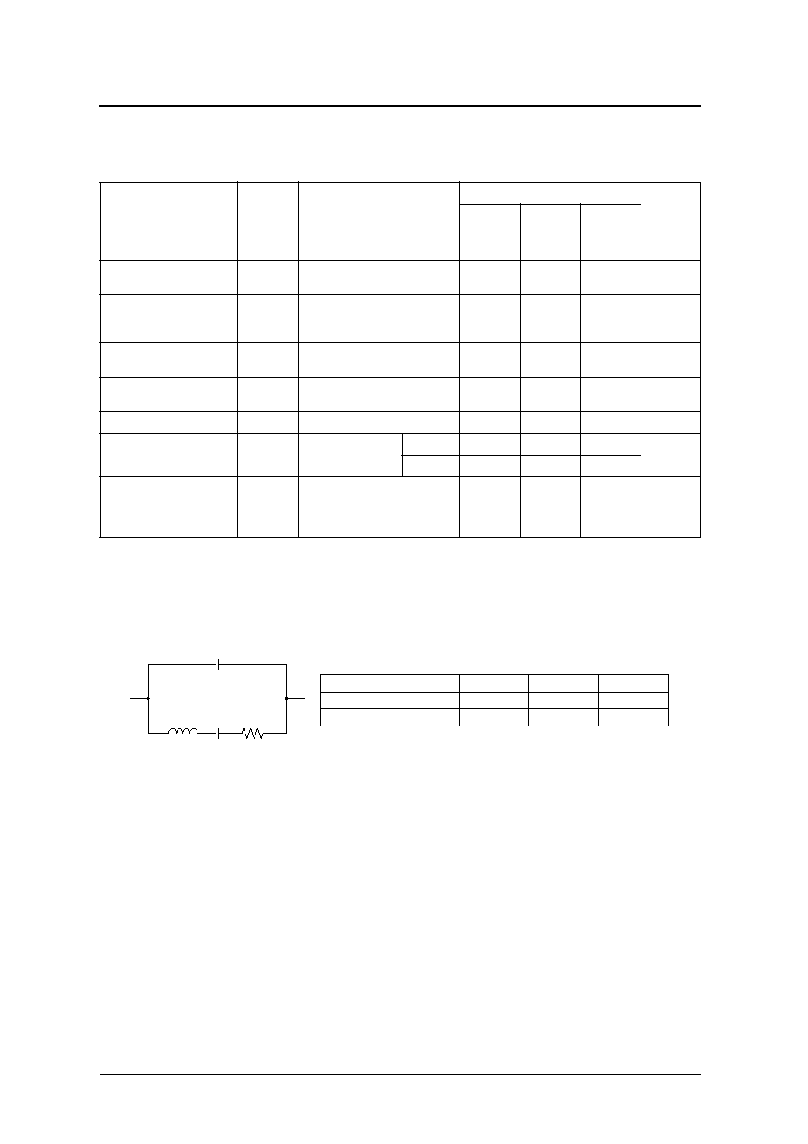
NPC STANDARD CRYSTAL DATA
P arameter
S y m b o l
Condition
Rating
Unit
m i n
typ
m a x
Output rise time
t
r
0.2V
D D
0.8V
D D
, measurement
circuit 1, load circuit 1, C
L
= 15pF
�
1
2.5
ns
Output fall time
t
f
0.8V
D D
0.2V
D D
, measurement
circuit 1, load circuit 1, C
L
= 15pF
�
1
2.5
ns
Output duty cycle
Duty
V
D D
= 3V, Ta = 25
�
C , measurement
circuit 1, load circuit 1, C
L
= 15pF,
f
1 6 6 . 6 M H z
4 0
�
6 0
%
Output disable delay time
1
1. Time from when INHN goes LOW until Q output goes high impedance.
t
P L Z
V
D D
= 3V, Ta = 25
�
C , measurement
circuit 1, load circuit 1, C
L
= 15pF
�
�
1 0 0
ns
Star tup time
2 ,3
2. Time from when either INHN goes LOW to HIGH or supply voltage V
D D
= 3.0V until normal signal output.
t
S Z L
V
D D
= 3V, Ta = 25
�
C , measurement
circuit 1, load circuit 1, C
L
= 15pF
�
1
�
m s
Oscillator frequency
f
Measurement circuit 1
2 0
�
4 0
M H z
Output frequency
f
O U T
Measurement circuit 1
V
D D
= 2.7V
1 0 0
�
1 2 5
M H z
V
D D
= 3.0V
1 0 0
�
166.6
Output clock jitter
3
3. Measured values using NPC characteristics standard evaluation board and standard cr ystal.
Jitter
V
D D
= 3V, Ta = 25
�
C , 25MHz cr ystal,
P0 = HIGH, P1 = LOW , measurement
circuit 1, load circuit 1,C
L
= 15pF,
peak-to-peak
�
1 0 0
�
ps
f (MHz)
R (
)
L (mH)
Ca (fF)
Cb (pF)
25
4.368
1.885
21.52
4.793
27
7.421
2.402
14.48
4.097
L
Ca
R
Cb

S M 5 0 5 0 A
NIPPON PRECISION CIRCUITS--6
MEASUREMENT CIRCUITS
Measurement Circuit 1
Measurement Circuit 2
Measurement Circuit 3
Measurement Circuit 4
Load Circuit 1
VDDQ
VSSQ
XT
Q
X'tal
XTN
INHN
I
DD
I
ST
A
VSS
VDD
VDDQ
VSSQ
P0, P1,
INHN
VSS
VDD
I
PR
V
IH
V
IL
V
DD
I
PR
(V
IL
= 0V)
R
UP2
=
I
PR
V
DD
= 3.0V
V
IH
= 2.1V
V
DD
V
IH
R
UP1
=
3.0V
V
A
VDDQ
VSSQ
XT
XTN
A
VSS
VDD
I
Rf
R
f
=
V
DD
I
Rf
VDDQ
VSSQ
Q
INHN
A
VSS
VDD
I
Z
V
OH
V
OL
V
I
Z
Q output
C
L
: 15pF
(Including probe capacitance)

S M 5 0 5 0 A
NIPPON PRECISION CIRCUITS--7
Switching Time Measurement Waveforms
Output duty level
Output duty cycle time
Output Disable Delay Time/Startup Time
0.8V
DD
0.2V
DD
0.8V
DD
0.2V
DD
t
r
t
f
Q output
DUTY measurement
voltage (0.5V
DD
)
T
W
DUTY measurement
voltage
(
0.5V
DD
)
Q output
T
W
T
DUTY= T
W
/ T 100 (%)
Q output
INHN
V
IL
t
PLZ
INHN input waveform
t
r =
t
f 10ns
V
IH
t
SZL
,,,,,,,,,
,,,,,,,,,
,,,,,,,,,
,,,,,,,,,
Hi-Z
,,,,,,,,
,,,,,,,,
,,,,,,,,
,,,,,,,,

S M 5 0 5 0 A
NIPPON PRECISION CIRCUITS--8
NIPPON PRECISION CIRCUITS INC. reserves the right to make changes to the products described in this data sheet in order to
improve the design or performance and to supply the best possible products. Nippon Precision Circuits Inc. assumes no responsibility fo r
the use of any circuits shown in this data sheet, conveys no license under any patent or other rights, and makes no claim that the circuits
are free from patent infringement. Applications for any devices shown in this data sheet are for illustration only and Nippon Precision
Circuits Inc. makes no claim or warranty that such applications will be suitable for the use specified without fur ther testing or modification.
The products described in this data sheet are not intended to use for the apparatus which influence human lives due to the failure or
malfunction of the products. Customers are requested to comply with applicable laws and regulations in effect now and hereinafter,
including compliance with expor t controls on the distribution or dissemination of the products. Customers shall not expor t, directly or
indirectly, any products without first obtaining required licenses and approvals from appropriate gover nment agencies.
NIPPON PRECISION CIRCUITS INC.
4-3, Fukuzumi 2-chome
Koto-ku, Tokyo 135-8430, Japan
Telephone: 03-3642-6661
Facsimile: 03-3642-6698
NC9921AE
2000.07
NIPPON PRECISION CIRCUITS INC.