CF5705 series
NIPPON PRECISION CIRCUITS--1
NIPPON PRECISION CIRCUITS INC.
Analog Watch Stepping Motor Driver
OVERVIEW
The CF5705 series is a low-current analog watch stepping motor driver CMOS IC with built-in 32.768 kHz
crystal oscillator circuit.
FEATURES
s
32.768 kHz crystal oscillator circuit
C
G
and C
D
built-in
s
-
3.6 to
-
1.2 V operating supply voltage range
s
Operating current consumption
� V
SS
= �1.55V, C
D
= 16pF: 250 nA (max)
� V
SS
= �2.8V, C
D
= 26pF: 1000 nA (max)
Note: Current consumption depends on the built-in capacitor.
s
Reset function
4 Hz and subsequent frequency dividers are reset
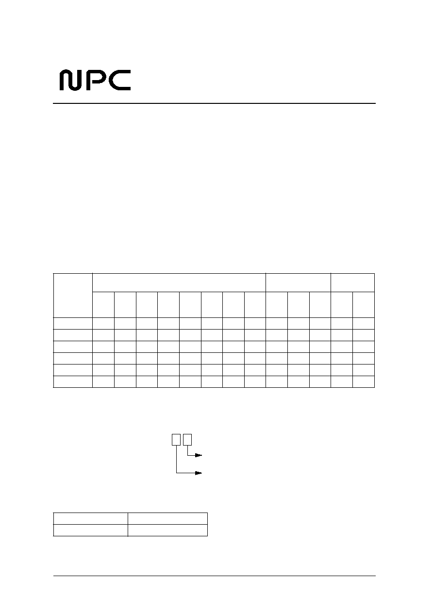
SERIES LINEUP
PART NUMBER GUIDE
ORDERING INFORMATION
V ersion
P ad coordinates
M o t o r
Built-in
capacitor
1
1. Parasitic capacitance is included. Parasitic capacitance: C
G
= C
D
= 4pF
1
2
3
4
5
6
7
8
C y c le
(Tcy/2)
s e c
Pulse
(Tpw)
s e c
Test
(Tcy)
s e c
C
G
p F
C
D
p F
C F 5 7 0 5 A A
X T
X T N
R E S E T
V S S
T E S T
O U T 2
O U T 1
V D D
1
4 . 9 m
1 2 5 m
4
1 6
C F 5 7 0 5 B C
V S S
R E S E T
X T
X T N
V D D
O U T 2
O U T 1
T E S T
2 5 0 m
2 3 . 4 m
1 2 5 m
4
2 6
C F 5 7 0 5 A D
X T
X T N
R E S E T
V S S
T E S T
O U T 2
O U T 1
V D D
1
2 3 . 4 m
1 2 5 m
4
3 0
C F 5 7 0 5 A E
X T
X T N
R E S E T
V S S
T E S T
O U T 2
O U T 1
V D D
2 0
5 . 9 m
1 2 5 m
4
1 6
C F 5 7 0 5 C F
V S S
T E S T
X T N
X T
V D D
O U T 2
O U T 1
R E S E T
1
4 . 9 m
6 2 . 5 m
4
1 6
C F 5 7 0 5 C G
V S S
T E S T
X T N
X T
V D D
O U T 2
O U T 1
R E S E T
1
3 . 9 m
6 2 . 5 m
4
1 6
D e vice
P a ck ag e
C F 5 7 0 5
��
Chip form
Function(Motor, Built-in capacitor)
CF5705
Pad coordinate

CF5705 series
NIPPON PRECISION CIRCUITS--2
PAD DIMENSIONS
(Top view)
PAD COORDINATES
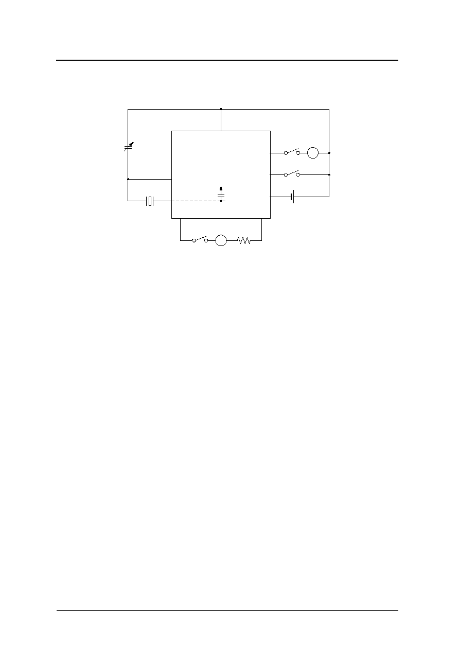
BLOCK DIAGRAM
PAD DESCRIPTION
Pin nu m b e r : Refer to Series lineup.
Chip size: 1.000
�
1.060 m m
Chip thickness: 220
�
m
P ad size: 100
�
100
�
m
R e verse side: V
D D
level
(0,0)
(1000,1060)
1
NPC
2
3
4
5
6
7
8
HA5705
N u m b e r
X (
�
m )
Y (
�
m )
1
1 5 5
7 8 5
2
1 5 5
5 9 7
3
1 5 5
3 6 3
4
1 5 5
1 7 5
5
8 4 4
1 7 5
6
8 4 4
3 6 3
7
8 4 4
6 9 4
8
8 4 4
8 8 2
XTN
TEST
RESET
XT
OUT2
OUT1
32kHz
Oscillator
Voltage
regulator
Divider and
Output buffer control
N a m e
Description
V S S
Negative supply voltage
V D D
P ositive supply voltage
X T
Cr ystal oscillator circuit input
X T N
Cr ystal oscillator circuit output
O U T 1
Stepping motor driver output 1
O U T 2
Stepping motor driver output 2
R E S E T
Reset input
T E S T
Test mode select. 512 Hz clock output

CF5705 series
NIPPON PRECISION CIRCUITS--3
SPECIFICATIONS
Absolute Maximum Ratings
V
DD
= 0 V
Recommended Operating Conditions
Electrical Characteristics
V
DD
= 0 V, T
a
= 25
�
C, X'tal C
I
= 55k
max
P arameter
S y m b o l
Rating
Unit
Supply voltage ra n g e
V
S S
-
5.0 to 0.3
V
Input voltage ra n g e
V
IN
V
S S
-
0.3 to 0.3
V
Storage temperature ra n g e
T
stg
-
40 to 125
�
C
P arameter
S y m b o l
Rating
Unit
Supply voltage
V
S S
-
3.6 to
-
1.2
V
O p e rating temperature
T
o p g
-
20 to 75
�
C
P arameter
S y m b o l
Condition
Rating
Unit
m i n
typ
m a x
O p e rating supply voltage
V
S S
-
2.0
-
-
1.2
V
O p e rating current consumption
1
1. Current consumption is measured in the measurement circuit (see next page).
I
D D
No load, V
S S
= �1.55V,
(C
T R
+ C
G
) = 15 pF, C
D
= 16 pF
�
0.15
0.25
� A
No load, V
S S
= �2.8V,
(C
T R
+ C
G
) = 24 pF, C
D
= 26 pF
�
0.40
1.00
� A
Reset input current
I
R S T
R E S E T : V
R S T
= V
D D
, V
S S
= �
1.55V
�
6
�
n A
R E S E T : V
R S T
= V
D D
, V
S S
= �2.8V
�
2 5
1 0 0
n A
Reset input resistance
R
R S T
V
R S T
=
-
1.35 V, V
S S
= �1.55V
1 5
3 5
6 0
k
V
R S T
=
-
2.6 V, V
S S
= �2.8V
5
1 5
5 0
k
Motor output current
I
M O T
R
L
= 2 k
, V
S S
=
-
1.55 V
0.7
�
�
m A
R
L
= 1 k
, V
S S
=
-
2.4 V
2.18
2.29
�
m A
Motor output cycle time
2
(normal mode)
2. Refer to Series lineup.
T
C Y
Refer to the SERIES LINEUP
s
Motor output cycle time
2
(test mode)
t
C Y
m s
Motor output pulsewidth
2
T
P W
m s
Oscillator start voltage
2
V
S TA
-
1.3
�
�
V
Oscillator start time
T
S TA
From supply ON to 512 Hz output
on T E S T
�
2
5
s
Frequency voltage deviation
f/f
V
S S
=
-
1.2
-
3.6 V, C
T R
= 5 p F
�
0.2
1
ppm/0.1V
Frequency deviation
3
3.
' = [f (1.55V) � f'
0
] / f'
0
(C
D
= 16pF)
' = [f (2.8V) � f'
0
] / f'
0
(C
D
= 26pF)
f'
0
: Oscillation frequency center value of Standard Deviation in the same measuring conditions
'
Built-in C
D
� 8
�
8
p p m
Built-in C
D
and C
G
� 16
�
1 6
p p m
Internal capacitance
2
C
G
, C
D
(C
G
+ C
D
) < 62 pF
Refer to the SERIES LINEUP
p F
CF5705 series
NIPPON PRECISION CIRCUITS--4
Measurement Circuit
Cr ystal: f = 32.768 kHz, CI = 20 k
, C0 = 1.3pF, C1 = 2.6fF
XTN
TEST
X'tal
VSS
VDD
RESET
C
TR
XT
OUT2
OUT1
A
C
D
A
I
MOT
R
L
I
RST

CF5705 series
NIPPON PRECISION CIRCUITS--5
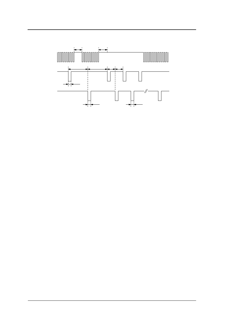
FUNCTIONAL DESCRIPTION
Motor Output Waveform
The motor output waveform cycle time and output pulsewidth are set by mask option.
Reset Function
Reset operation
A reset operation occurs when RESET is held HIGH
(V
DD
) for a period of 93.75 ms or greater, otherwise
the reset is ignored. When the reset pulse is valid, the
4 Hz and subsequent frequency dividers are reset.
Reset Release
When the reset is released, the first output pulse
occurs on the output pin opposite the output pin
where the preceding motor drive output pulse
occurred; first pulse occurs on OUT1 if previous
motor drive pulse occurred on OUT2, and vice versa.
A delay of T
CY
/2
-
0.125 to T
CY
/2 takes place from
when reset is released until the first output pulse
occurs.
OUT1
OUT2
T
PW
T
CY
/2
V
DD
V
SS
T
PW
T
CY
/2
V
DD
V
SS
T < T
ON
T > T
ON
V
DD
V
SS
RESET
(open)
OUT1
T
PW
V
DD
V
SS
OUT2
T
CY
/2
T
CY
/2
V
DD
V
SS
T
D
CF5705 series
NIPPON PRECISION CIRCUITS--6
Test Function
Normal mode (TEST = open circuit)
In test mode, a 512 Hz rectangular wave is output on
TEST. Note that the output load (probe) must be
greater than 10 M
and less than 20 pF. The motor
drive outputs on OUT1 and OUT2 continue to oper-
ate normally.
Test mode 1 (TEST = V
DD
)
Test mode 1 is invoked when TEST is held HIGH for
a minimum of 2 cycles of the 512
Hz clock
(T
CH
> 3.9 ms), otherwise it is ignored. In test mode
1, high-speed motor output operation occurs, with
the cycle time set by mask option to 62.5 or 125 ms.
Test mode 2 (TEST = V
SS
)
Test mode 2 is a dedicated IC test mode. In test mode
2, the device operates at 32-times speed, with the
supply voltage connected directly to the oscillator
circuit. Note that if a reset input occurs, the internal
operation is reset and device output stops. Once
operation stops, normal operation is not restored
until TEST is either open circuit or goes LOW.
OUT1
OUT2
T
PW
T
CY
/2
V
DD
V
SS
T
PW
T
CY
/2
V
DD
V
SS
t
CY
/2
t
CY
/2
T
PW
T < T
ch
T > T
ch
V
DD
V
SS
TEST

CF5705 series
NIPPON PRECISION CIRCUITS--7
NIPPON PRECISION CIRCUITS INC. reserves the right to make changes to the products described in this data sheet in order to
improve the design or performance and to supply the best possible products. Nippon Precision Circuits Inc. assumes no responsibility fo r
the use of any circuits shown in this data sheet, conveys no license under any patent or other rights, and makes no claim that the circuits
are free from patent infringement. Applications for any devices shown in this data sheet are for illustration only and Nippon Precision
Circuits Inc. makes no claim or warranty that such applications will be suitable for the use specified without fur ther testing or modification.
The products described in this data sheet are not intended to use for the apparatus which influence human lives due to the failure or
malfunction of the products. Customers are requested to comply with applicable laws and regulations in effect now and hereinafter,
including compliance with expor t controls on the distribution or dissemination of the products. Customers shall not expor t, directly or
indirectly, any products without first obtaining required licenses and approvals from appropriate gover nment agencies.
NIPPON PRECISION CIRCUITS INC.
4-3, Fukuzumi 2-chome
Koto-ku, Tokyo 135-8430, Japan
Telephone: 03-3642-6661
Facsimile: 03-3642-6698
NC9815AE
2000.07
NIPPON PRECISION CIRCUITS INC.