 | –≠–ª–µ–∫—Ç—Ä–æ–Ω–Ω—ã–π –∫–æ–º–ø–æ–Ω–µ–Ω—Ç: CF5760DA | –°–∫–∞—á–∞—Ç—å:  PDF PDF  ZIP ZIP |
CF5760 series
NIPPON PRECISION CIRCUITS--1
NIPPON PRECISION CIRCUITS INC.
CMOS Analog Clock IC
OVERVIEW
The CF5760 series devices are analog clock ICs that derive their timing from a 32.768 kHz oscillator element.
They feature a reset function (optional seconds control function) which can be used to maintain accurate time.
Various alarm functions and motor outputs are available to match a wide range of clock specifications.
FEATURES
I
1.2 to 2.0V operating supply voltage
I
1.2µA (typ) / 1.5V current consumption
I
32.768 kHz oscillator circuit
I
Oscillator capacitance C
G
and C
D
built-in
I
Alarm output function
I
Reset function (optional seconds control function)
I
Input chattering elimination function (AI/R)
I
Chip form (CF5760
◊◊
)
PAD LAYOUT
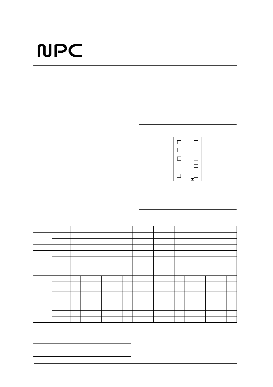
SERIES CONFIGURATION
ORDERING INFORMATION
Top view
Chip size: 0.76
◊
1.21 mm
Chip thickness: 300 ± 30 µm
P ad size: 100
◊
100 µm
R e verse side: V
D D
level
1
XT
VSS
(0,0)
2
3
4
5
9
8
7
6
XTN
AON
AO
VDD
O1
AI/R
O2
HA5760
C F 5 7 6 0 A A
C F 5 7 6 0 B A
C F 5 7 6 0 C C
C F 5 7 6 0 DA
C F 5 7 6 0 E A
C F 5 7 6 0 F C
C F 5 7 6 0 H A
C F 5 7 6 0 J A
Built-in
capacitance
1
1. Built-in capacitance includes the parasitic capacitance.
C
G
(pF)
3
3
3
3
3
3
3
3
C
D
(pF)
2 5
2 5
3 3
2 5
2 5
3 3
2 5
2 5
Alarm input/reset input level
H I G H / L OW
H I G H / L OW
L O W / H I G H
L O W / H I G H
≠ / L OW
L O W / H I G H
L O W / H I G H
L O W / H I G H
Motor output
Active level
L O W
L O W
H I G H
L O W
≠
≠
H I G H
≠
Needle period
t
C Y
(s)
1
1
1
1
1
0.0625
1
0.0625
Pulsewidth
t
P W
(ms)
23.4
23.4
31.25
27.3
1 0 0 0
62.5
46.875
62.5
Alarm output
Pins
A O
A O N
A O
A O N
A O
A O N
A O
A O N
A O
A O N
A O
A O N
A O
A O N
A O
A O N
Active level
H I G H
L O W
H I G H
F
(32kHz)
H I G H
L O W
H I G H
F
(32kHz)
≠
≠
H I G H
L O W
H I G H
L O W
H I G H
F
(32kHz)
Frequency
f
P W
(kHz)
4
4
D C
≠
2
2
D C
≠
≠
≠
2
2
2
2
D C
≠
Modulation
f
C Y
(Hz)
8
8
≠
≠
8 + 1
8 + 1
≠
≠
≠
≠
8 + 1
8 + 1
8 + 1
8 + 1
≠
≠
I
O H
min (
µ
A)
9 0 0
9 0 0
9 0 0
1 0
9 0 0
9 0 0
9 0 0
1 0
≠
≠
9 0 0
9 0 0
9 0 0
9 0 0
9 0 0
1 0
I
O L
min (
µ
A)
9 0 0
9 0 0
1 0
1 0
9 0 0
9 0 0
1 0
1 0
≠
≠
9 0 0
9 0 0
9 0 0
9 0 0
1 0
1 0
D e vice
P a ck ag e
C F 5 7 6 0
◊◊
Chip form

CF5760 series
NIPPON PRECISION CIRCUITS--2
BLOCK DIAGRAM
PAD DESCRIPTION/DIMENSIONS
N o .
N a m e
Description
Dimensions (µm)
X
Y
1
V D D
Supply
1 5 5
1 0 6 5
2
AI/R
Alarm input and reset input
1 5 5
8 5 4
3
O 1
Motor output 1
1 5 5
6 2 0
4
O 2
Motor output 2
1 4 5
1 4 5
5
V S S
G r o u n d
6 1 5
1 4 5
6
A O
Alarm output 1
6 1 5
3 2 5
7
A O N
Alarm output 2
6 1 5
5 0 5
8
X T N
Oscillator output
6 1 5
7 4 6
9
X T
Oscillator input
6 1 5
1 0 6 5
7 Stage
Divider
9 Stage
Divider
Reset
Input
Alarm
Input
Alarm Output
Control
Motor Output
Control
VDD
VSS
AO
AON
O1
O2
XT
AI/R
XTN
C
D
C
G

CF5760 series
NIPPON PRECISION CIRCUITS--3
SPECIFICATIONS
Absolute Maximum Ratings
Electrical Characteristics
T
a
= 25
∞
C, V
DD
= 1.5V, V
SS
= 0V, C
G
= 23pF, C
D
= 25pF, X'tal (f
0
= 32.768kHz, C
I
= 50k
max) unless oth-
erwise noted
P arameter
S y m b o l
Condition
Rating
Unit
Supply voltage ra n g e
V
D D
-
V
S S
-
0.3 to 5.0
V
Input voltage ra n g e
V
IN
V
S S
V
IN
V
D D
V
O p e rating temperature ra n g e
T
opr
-
30 to 80
∞
C
Storage temperature ra n g e
T
stg
-
65 to 150
∞
C
P arameter
S y m b o l
Condition
Rating
Unit
m i n
typ
m a x
O p e rating voltage
V
D D
1.2
≠
2.0
V
Current consumption
I
D D
O1 = O2 = open
≠
1.2
4.0
µ A
Oscillator start-up time
t
S TA
V
D D
= 1.2V
≠
≠
5.0
s
Motor output current
I
M O T
V
D D
= 1.2V, R
L
= 200
1
1. R
L
is the load resistance connected between O1 and O2.
4.0
≠
≠
m A
AI/R HIGH-level input current
I
IH
V
D D
= 1.5V
2
4
8
µ A
AI/R LOW -level input current
I
IL
V
D D
= 1.5V
2
4
8
µ A
Oscillator frequency stability
f/f
V
D D
= 1.2 to 2.0V
≠
0.5
1.0
ppm/0.1V
Alarm L O W -level output current
2
(AO , AO N )
2. CF5760AA/ CC/ FC/ HA: If the outputs (AO or AON) are shor t circuit, the output current is I
A O
900
µ
A.
I
O L 1
V
D D
= 1.5V, V
O L
= 0.75V
9 0 0
2 0 0 0
≠
µ A
I
O L 2
V
D D
= 1.5V, V
O L
= 0.75V
1 0
3 0
≠
µ A
Alarm HIGH-level output current
2
(AO , AO N )
I
O H 1
V
D D
= 1.5V, V
O H
= 0.75V
9 0 0
2 0 0 0
≠
µ A
I
O H 2
V
D D
= 1.5V, V
O H
= 0.75V
1 0
3 0
≠
µ A
F output voltage
3
3. The F output voltage rating, V F, when a load capacitance, C
L
, is connected between pin F and V S S , is the difference voltage between the center volt-
a g e, 0.5V
D D
, and the peak voltage.
V
F
V
D D
= 1.2V, C
L
= 50pF
0.4
≠
≠
V
Internal capacitance
4
4. C
G
is the capacitance between V D D a n d X T. C
D
is the capacitance between V D D a n d X T N .
C
G
Refer to the SERIES LINEUP
p F
C
D
p F

CF5760 series
NIPPON PRECISION CIRCUITS--4
FUNCTIONAL DESCRIPTION
Motor Output
Motor output waveform (step motor driver)
Motor output waveform (sweep motor driver)
Input Chattering Elimination Function (AI/R)
A bounce delay is provided on the AI/R input to eliminate erroneous operation caused by input bounce (chat-
tering).
Input Control Functions
When AI/R is open circuit, a 256Hz signal is output.
When AI/R is HIGH or LOW, it selects the alarm (HIGH)/reset (LOW) function or reset (HIGH)/alarm (LOW)
function depending on the version.
O1
(Active High)
O2
(Active High)
t
PW
t
PW
t
CY
t
CY
: Needle period
t
PW
: Pulse width
t
CY
t
O N
< 62.5ms: input is ignored.
62.5
t
O N
125ms: indeterminate
t
O N
> 125ms: input is accepted.
O1
O2
t
CY
62.5ms
t
CY
: Needle period
t
PW
: Pulse width
t
CY
62.5ms
t
PW
62.5ms
t
PW
62.5ms
t
ON
AI/R
(Active Low)
CF5760 series
NIPPON PRECISION CIRCUITS--5
Reset Function (optional seconds control function)
When AI/R goes active level for a reset, the motor output stops. When the reset is released, the first motor out-
put pulse occurs on the output pin opposite to that which had the last output pulse immediately before the reset.
Alarm Output
Alarm output waveform
F Output Function
The AON pin may be replaced by the F pin which is used to output a 32kHz signal (unaffected by the reset
function).
O1
(Active High)
O2
(Active High)
t
PW
t
PW
t
CY
t
CY
AI/R
(Active Low)
t
CY
+0
-125msec
t
ON
*1: Opposite phase to AO .
f
P W
= alarm fundamental frequency
f
C Y
= alarm modulation frequency
AO
(Active High)
AI/R
(Active High)
AON
(Active Low)
f
PW
(Hz)
f
CY
(Hz)
t
ON
*1