 | –≠–ª–µ–∫—Ç—Ä–æ–Ω–Ω—ã–π –∫–æ–º–ø–æ–Ω–µ–Ω—Ç: CF5760 | –°–∫–∞—á–∞—Ç—å:  PDF PDF  ZIP ZIP |
CF5760 series
NIPPON PRECISION CIRCUITS INC.--1
CMOS Analog Clock IC
OVERVIEW
The CF5760 series are analog clock ICs that derive their timing from a 32.768 kHz oscillator element. They
feature a reset function (optional seconds control function) which can be used to maintain accurate time. Vari-
ous alarm functions and motor outputs are available to match a wide range of clock specifications.
FEATURES
I
1.2 to 2.0V operating supply voltage
I
1.2µA (typ) / 1.5V current consumption
I
32.768 kHz oscillator circuit
I
Oscillator capacitance C
G
and C
D
built-in
I
Alarm output function
I
Reset function (optional seconds control function)
I
Input chattering elimination function (AI/R)
I
Chip form (CF5760
◊◊
)
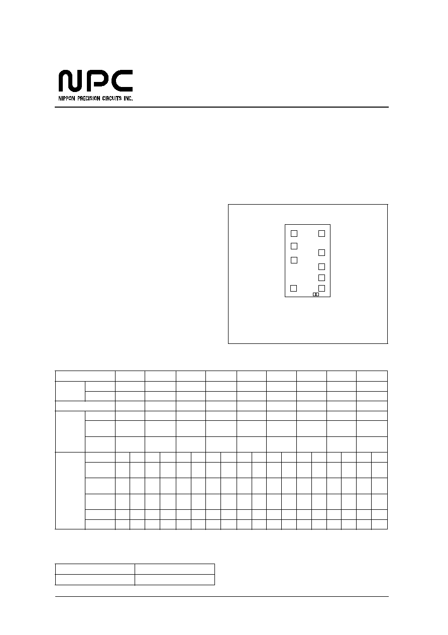
PAD LAYOUT
SERIES CONFIGURATION
ORDERING INFORMATION
Top view
Chip size: 0.76
◊
1.21 mm
Chip thickness: 300 ± 30 µm
Pad size: 100
◊
100 µm
Reverse side: V
DD
level
1
XT
VSS
(0,0)
2
3
4
5
9
8
7
6
XTN
AON
AO
VDD
O1
AI/R
O2
HA5760
CF5760AA
CF5760BA
CF5760CC
CF5760DA
CF5760EA
CF5760FC CF5760GB CF5760HA
CF5760JA
Built-in
capacitance
1
1. Built-in capacitance includes the parasitic capacitance.
C
G
[pF]
3
3
3
3
3
3
27
3
3
C
D
[pF]
25
25
33
25
25
33
26
25
25
Alarm input/reset input level
HIGH/LOW
HIGH/LOW
LOW/HIGH
LOW/HIGH
≠/LOW
LOW/HIGH
LOW/HIGH
LOW/HIGH
LOW/HIGH
Motor output
Active level
LOW
LOW
HIGH
LOW
≠
≠
HIGH
HIGH
≠
Needle period
t
CY
[s]
1
1
1
1
1
0.0625
1
1
0.0625
Pulsewidth
t
PW
[ms]
23.4
23.4
31.25
27.3
1000
62.5
31.25
46.875
62.5
Alarm output
Pins
AO
AON
AO
AON
AO
AON
AO
AON
AO
AON
AO
AON
AO
AON
AO
AON
AO
AON
Active level
HIGH LOW HIGH
F
(32kHz)
HIGH LOW HIGH
F
(32kHz)
≠
≠
HIGH LOW HIGH LOW HIGH LOW HIGH
F
(32kHz)
Frequency
f
PW
[kHz]
4
4
DC
≠
2
2
DC
≠
≠
≠
2
2
2
2
2
2
DC
≠
Modulation
f
CY
[Hz]
8
8
≠
≠
8 + 1
8 + 1
≠
≠
≠
≠
8 + 1
8 + 1
8 + 1
8 + 1
8 + 1
8 + 1
≠
≠
I
OH
min [
µ
A]
900
900
900
10
900
900
900
10
≠
≠
900
900
900
900
900
900
900
10
I
OL
min [
µ
A]
900
900
10
10
900
900
10
10
≠
≠
900
900
10
10
900
900
10
10
Device
Package
CF5760
◊◊
Chip form

CF5760 series
NIPPON PRECISION CIRCUITS INC.--2
BLOCK DIAGRAM
PAD DESCRIPTION/DIMENSIONS
No.
Name
Description
Dimensions [µm]
X
Y
1
VDD
Supply
155
1065
2
AI/R
Alarm input and reset input
155
854
3
O1
Motor output 1
155
620
4
O2
Motor output 2
145
145
5
VSS
Ground
615
145
6
AO
Alarm output 1
615
325
7
AON
Alarm output 2
615
505
8
XTN
Oscillator output
615
746
9
XT
Oscillator input
615
1065
7 Stage
Divider
9 Stage
Divider
Reset
Input
Alarm
Input
Alarm Output
Control
Motor Output
Control
VDD
VSS
AO
AON
O1
O2
XT
AI/R
XTN
C
D
C
G

CF5760 series
NIPPON PRECISION CIRCUITS INC.--3
SPECIFICATIONS
Absolute Maximum Ratings
Electrical Characteristics
T
a
= 25
∞
C, V
DD
= 1.5V, V
SS
= 0V, C
G
= 23pF, C
D
= 25pF, X'tal (f
0
= 32.768kHz, C
I
= 50k
max) unless oth-
erwise noted
Parameter
Symbol
Condition
Rating
Unit
Supply voltage range
V
DD
-
V
SS
-
0.3 to 5.0
V
Input voltage range
V
IN
V
SS
V
IN
V
DD
V
Operating temperature range
T
opr
-
30 to 80
∞
C
Storage temperature range
T
stg
-
65 to 150
∞
C
Parameter
Symbol
Condition
Rating
Unit
min
typ
max
Operating voltage
V
DD
1.2
≠
2.0
V
Current consumption
I
DD
O1 = O2 = open
≠
1.2
4.0
µA
Oscillator start-up time
t
STA
V
DD
= 1.2V
≠
≠
5.0
s
Motor output current
I
MOT
V
DD
= 1.2V, R
L
= 200
1
1. R
L
is the load resistance connected between O1 and O2.
4.0
≠
≠
mA
AI/R HIGH-level input current
I
IH
V
DD
= 1.5V
2
4
8
µA
AI/R LOW-level input current
I
IL
V
DD
= 1.5V
2
4
8
µA
Oscillator frequency stability
f/f
V
DD
= 1.2 to 2.0V
≠
0.5
1.0
ppm/0.1V
Alarm LOW-level output current
2
(AO, AON)
2. CF5760AA/ CC/ FC/ HA: If the outputs (AO or AON) are short circuit, the output current is I
AO
900
µ
A.
I
OL1
V
DD
= 1.5V, V
OL
= 0.75V
900
2000
≠
µA
I
OL2
V
DD
= 1.5V, V
OL
= 0.75V
10
30
≠
µA
Alarm HIGH-level output current
2
(AO, AON)
I
OH1
V
DD
= 1.5V, V
OH
= 0.75V
900
2000
≠
µA
I
OH2
V
DD
= 1.5V, V
OH
= 0.75V
10
30
≠
µA
F output voltage
3
3. The F output voltage rating, V
F
, when a load capacitance, C
L
, is connected between pin F and VSS, is the difference voltage between the center volt-
age, 0.5V
DD
, and the peak voltage.
V
F
V
DD
= 1.2V, C
L
= 50pF
0.4
≠
≠
V
Internal capacitance
4
4. C
G
is the capacitance between VDD and XT. C
D
is the capacitance between VDD and XTN.
C
G
Refer to the SERIES LINEUP
pF
C
D
pF

CF5760 series
NIPPON PRECISION CIRCUITS INC.--4
FUNCTIONAL DESCRIPTION
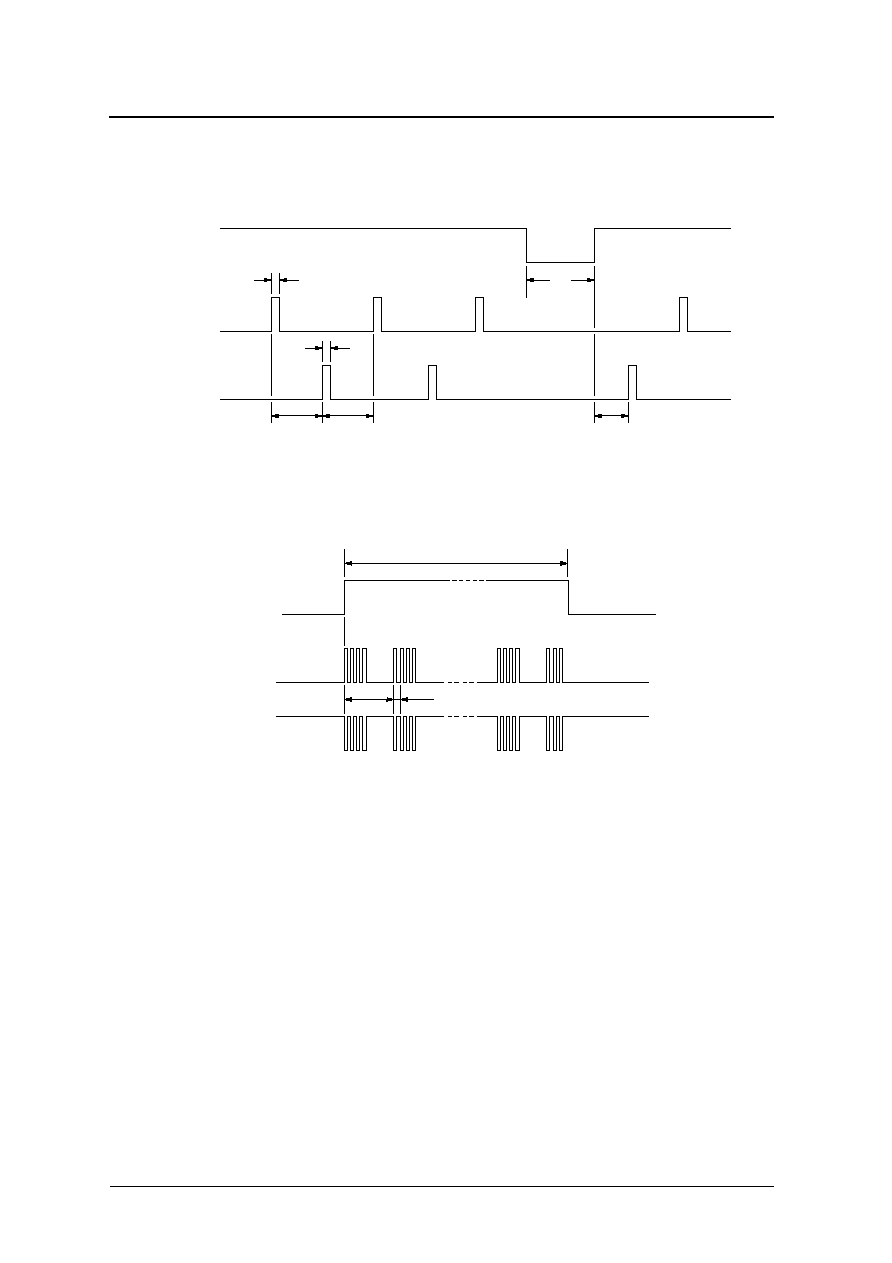
Motor Output
Motor output waveform (step motor driver)
Motor output waveform (sweep motor driver)
Input Chattering Elimination Function (AI/R)
A bounce delay is provided on the AI/R input to eliminate erroneous operation caused by input bounce (chat-
tering).
Input Control Functions
When AI/R is open circuit, a 256Hz signal is output.
When AI/R is HIGH or LOW, it selects the alarm (HIGH)/reset (LOW) function or reset (HIGH)/alarm (LOW)
function depending on the version.
O1
(Active High)
O2
(Active High)
t
PW
t
PW
t
CY
t
CY
: Needle period
t
PW
: Pulse width
t
CY
t
ON
< 62.5ms: input is ignored.
62.5
t
ON
125ms: indeterminate
t
ON
> 125ms: input is accepted.
O1
O2
t
CY
62.5ms
t
CY
: Needle period
t
PW
: Pulse width
t
CY
62.5ms
t
PW
62.5ms
t
PW
62.5ms
t
ON
AI/R
(Active Low)
CF5760 series
NIPPON PRECISION CIRCUITS INC.--5
Reset Function (optional seconds control function)
When AI/R goes active level for a reset, the motor output stops. When the reset is released, the first motor out-
put pulse occurs on the output pin opposite to that which had the last output pulse immediately before the reset.
Alarm Output
Alarm output waveform
F Output Function
The AON pin may be replaced by the F pin which is used to output a 32kHz signal (unaffected by the reset
function).
O1
(Active High)
O2
(Active High)
t
PW
t
PW
t
CY
t
CY
AI/R
(Active Low)
t
CY
+0
-125msec
t
ON
*1: Opposite phase to AO.
f
PW
= alarm fundamental frequency
f
CY
= alarm modulation frequency
AO
(Active High)
AI/R
(Active High)
AON
(Active Low)
f
PW
(Hz)
f
CY
(Hz)
t
ON
*1