CF5761 series
NIPPON PRECISION CIRCUITS INC.--1
CMOS Analog Clock IC with Alarm Function
OVERVIEW
The CF5761 series are analog clock ICs with alarm functions that derive their timing from a standard
32.768kHz oscillator element. Two kinds of alarm output are available and can be selected using a control pin.
The series lineup comprises devices with various alarm patterns and motor outputs for a wide range of clock
specifications. They support convenient functions, such as input chattering elimination circuit and power-on
clear functions. They are fabricated using Molybdenum-gate CMOS process, realizing low power consump-
tion.
FEATURES
I
32.768kHz fundamental frequency oscillator
I
Feedback resistor and oscillator capacitor C
D
built-in
I
Supports various alarms: piezo-alarm, electromag-
netic speaker
I
Snooze function
I
Switchable alarm function using SEL pin
I
Alarm auto-stop function (see series lineup)
I
Input chattering elimination circuit (SEL, AI, SN)
I
Test function
I
1.2 to 3.6V operating supply voltage
I
Chip form (CF5761
��
)
I
Molybdenum-gate CMOS process
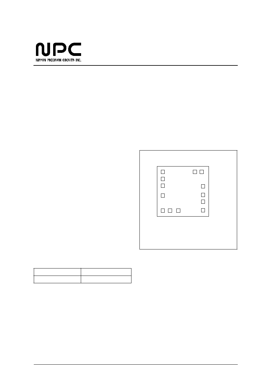
PAD LAYOUT
(Unit:
�
m)
ORDERING INFORMATION
Chip size: 1.41
�
1.37 mm
Chip thickness: 300 � 30 �m
Pad size: 100
�
100 �m
Reverse side: V
DD
level
(0,0)
(1410, 1370)
HA5761
XTN
AO1
NPC
AO3 SEL
AO2
VSS
O2
O1
XT
SN
AI
TI
VDD
1
2
3
4
5
6
7
8
10
9
11
12
13
Device
Package
CF5761
��
Chip form
CF5761 series
NIPPON PRECISION CIRCUITS INC.--2
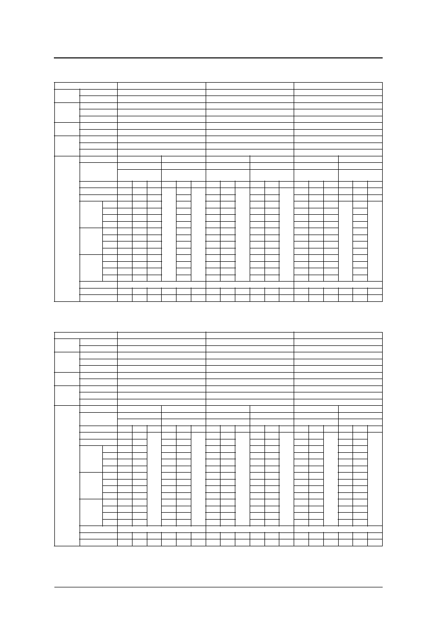
SERIES LINEUP
CF5761CA
CF5761EA
CF5761HA
Built-in
capacitance
1
1. C
G
and C
D
built-in parasitic capacitance (C
G
= C
D
= 4pF)
C
G
[pF]
4
4
4
C
D
[pF]
27
27
27
Motor output
Active level
�
LOW
LOW
Needle period t
CY
[s]
0.0625 (8Hz sweep)
1
10
Pulsewidth t
PW
[ms]
62.5 (50% duty)
23.4
13.7
AI input
Active level
HIGH (pull-down)
HIGH (pull-down)
HIGH (pull-down)
Bounce delay [ms]
62.5
62.5
62.5
SN input
Active level
HIGH (pull-down)
HIGH (pull-down)
HIGH (pull-down)
Snooze time t
SNZ
[s]
300
300
300
Bounce delay [ms]
62.5
62.5
62.5
Alarm output
SEL pin
LOW
HIGH
LOW
HIGH
LOW
HIGH
Application
Simple alarm
Simple alarm
Step tone alarm
Simple alarm
Simple alarm
Simple alarm
AO1, AO3: tone
AO2: motor bell
AO1, AO3: tone
AO2: Magnet speaker
AO1, AO2: motor bell
AO1, AO2: motor bell
AO1, AO3: tone
AO1, AO3: tone
Pin
AO1
AO2
AO3
AO1
AO2
AO3
AO1
AO2
AO3
AO1
AO2
AO3
AO1
AO2
AO3
AO1
AO2
AO3
Active level
H
H
L
64Hz
clock
output
H
32Hz
clock
output
H
L
32kHz
F
output
H
L
32kHz
F
output
H
H
L
H
H
L
Frequency f
PW
[kHz]
4
DC
4
2
�
�
DC
DC
4
�
4
4
�
4
Modulation
f
CY
[Hz]
Step 1
8
�
8
8
1+2+4+8
1+2+4+8
�
�
1+16
1+16
1+16
See special timing in functional descr
iption.
�
See special timing in functional descr
iption.
Step 2
�
�
�
�
1+2+8
1+2+8
�
�
�
�
�
�
Step 3
�
�
�
�
1+8
1+8
�
�
�
�
�
�
Step 4
�
�
�
�
DC
DC
�
�
�
�
�
�
Duty [%]
Step 1
50
�
50
50
50
50
�
�
50
�
50
�
Step 2
�
�
�
�
50
50
�
�
�
�
�
�
Step 3
�
�
�
�
50
50
�
�
�
�
�
�
Step 4
�
�
�
�
�
�
�
�
�
�
�
�
Step time [s]
Step 1
�
�
�
�
0�8
0�8
�
�
�
�
�
�
Step 2
�
�
�
�
8�16
8�16
�
�
�
�
�
�
Step 3
�
�
�
�
16�24
16�24
�
�
�
�
�
�
Step 4
�
�
�
�
24�
24�
�
�
�
�
�
�
Auto-stop [s]
None
None
None
I
OH
[mA] min.
-
0.9
-
0.9
-
0.9
-
0.9
-
0.9
-
0.9
-
0.9
-
0.01
-
0.01
-
0.9
-
0.01
-
0.01
-
0.9
-
0.9
-
0.9
-
0.9
-
0.9
-
0.9
I
OL
[mA] min.
0.9
0.01
0.9
0.9
0.01
0.9
0.01
0.9
0.01
0.01
0.9
0.01
0.9
0.01
0.9
0.9
0.01
0.9
CF5761LB
CF5761MB
CF5761NB
Built-in
capacitance
1
1. C
G
and C
D
built-in parasitic capacitance (C
G
= C
D
= 4pF)
C
G
[pF]
4
4
4
C
D
[pF]
34
34
34
Motor output
Active level
LOW
�
LOW
Needle period t
CY
[s]
1
0.0625 (8Hz sweep)
1
Pulsewidth t
PW
[ms]
31.3
62.5 (50% duty)
23.4
AI input
Active level
LOW (pull-up)
LOW (pull-up)
LOW (pull-up)
Bounce delay [ms]
62.5
62.5
62.5
SN input
Active level
LOW (pull-up)
LOW (pull-up)
LOW (pull-up)
Snooze time t
SNZ
[s]
300
300
300
Bounce delay [ms]
62.5
62.5
62.5
Alarm output
SEL pin
LOW
HIGH
LOW
HIGH
LOW
HIGH
Application
Step volume alarm
Simple alarm
Step volume alarm
Simple alarm
Step volume alarm
Step volume alarm
AO1, AO2: tone
AO1, AO2: motor bell
AO1, AO2: tone
AO1, AO2: motor bell
AO1, AO2: tone
AO1, AO2: tone
Pin
AO1
AO2
AO3
AO1
AO2
AO3
AO1
AO2
AO3
AO1
AO2
AO3
AO1
AO2
AO3
AO1
AO2
AO3
Active level
H
L
Not
used
H
H
Not
used
H
L
Not
used
H
H
Not
used
H
L
Not
used
H
L
Not
used
Frequency f
PW
[kHz]
2
2
DC
DC
2
2
DC
DC
4
4
2
2
Modulation
f
CY
[Hz]
Step 1
1+8
1+8
�
�
1+8
1+8
�
�
1+8
1+8
1+8
1+8
Step 2
1+8
1+8
�
�
1+8
1+8
�
�
1+8
1+8
1+8
1+8
Step 3
1+8
1+8
�
�
1+8
1+8
�
�
1+8
1+8
1+8
1+8
Step 4
�
�
�
�
1+8
1+8
�
�
�
�
�
�
Duty [%]
Step 1
6.25
6.25
�
�
6.25
6.25
�
�
6.25
6.25
12.5
12.5
Step 2
12.5
12.5
�
�
12.5
12.5
�
�
12.5
12.5
25
25
Step 3
50
50
�
�
25
25
�
�
50
50
50
50
Step 4
�
�
�
�
50
50
�
�
�
�
�
�
Step time [s]
Step 1
0�8
0�8
�
�
0�4
0�4
�
�
0�8
0�8
0�8
0�8
Step 2
8�16
8�16
�
�
4�8
4�8
�
�
8�16
8�16
8�16
8�16
Step 3
16�
16�
�
�
8�12
8�12
�
�
16�
16�
16�
16�
Step 4
�
�
�
�
12�
12�
�
�
�
�
�
�
Auto-stop [s]
300
300
300
I
OH
[mA] min.
-
0.9
-
0.9
-
0.9
-
0.9
-
0.9
-
0.9
-
0.9
-
0.9
-
0.9
-
0.9
-
0.9
-
0.9
-
0.9
-
0.9
-
0.9
-
0.9
-
0.9
-
0.9
I
OL
[mA] min.
0.9
0.9
0.9
0.9
0.9
0.9
0.9
0.9
0.9
0.9
0.9
0.9
0.9
0.9
0.9
0.9
0.9
0.9
CF5761 series
NIPPON PRECISION CIRCUITS INC.--3
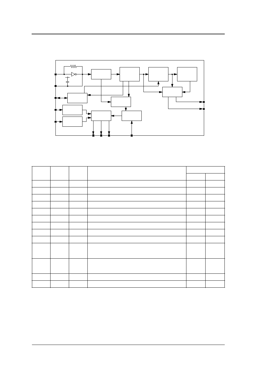
BLOCK DIAGRAM
PAD DESCRIPTION and DIMENSIONS
Number
Name
I/O
Function
Pad dimensions
X [�m]
Y [�m]
1
O1
O
Movement motor drive output 1 (CMOS output)
155
1215
2
O2
O
Movement motor drive output 2 (CMOS output)
155
1023
3
VSS
�
Ground
155
835
4
AO2
O
Alarm output 2
155
567
5
AO1
O
Alarm output 1
155
155
6
AO3
O
Alarm output 3
351
155
7
SEL
I
Alarm function select. Pull-down resistor built-in
583
155
8
XTN
O
Crystal oscillator output. Oscillator capacitance C
D
built-in
1255
166
9
XT
I
Crystal oscillator input. Crystal connected between XT and XTN
1255
399
10
SN
I
Snooze input
Pull-down resistor built-in (CF5761CA, EA, HA)
Pull-up resistor built-in (CF5761LB, MB, NB)
1255
587
11
AI
I
Alarm input
Pull-down resistor built-in (CF5761CA, EA, HA)
Pull-up resistor built-in (CF5761LB, MB, NB)
1255
821
12
T1
I/O
Test pin
1217
1215
13
VDD
�
Supply
1029
1215
XT
6-stage
divider
5-stage
divider
4-stage
divider
4-stage
divider
XTN
T1
AI
SN
Test control
Alarm input
control
Snooze input
control
Alarm output
control
Alarm pattern
select
Alarm pattern
control
Motor output
control
AO2
AO1
AO3
SEL
O1
O2

CF5761 series
NIPPON PRECISION CIRCUITS INC.--4
SPECIFICATIONS
Absolute Maximum Ratings
Electrical Characteristics
1.5V operation
T
a
= 25
�
C, V
SS
= 0V, V
DD
= 1.5V, X'tal (f
0
= 32.768kHz, C
I
= 35k
max, C
G
= 20pF) unless otherwise noted
Parameter
Symbol
Condition
Rating
Unit
Supply voltage range
V
DD
-
V
SS
-
0.3 to 5.0
V
Input voltage range
V
IN
V
SS
to V
DD
V
Operating temperature range
T
opr
-
30 to 80
�
C
Storage temperature range
T
stg
-
65 to 150
�
C
Parameter
Symbol
Condition
Rating
Unit
min
typ
max
Operating voltage
V
DD
1.2
1.5
3.6
V
Oscillator startup time
1
1. Measured using standard circuits.
t
1
V
DD
= 1.2V
�
�
5.0
s
Frequency voltage characteristic
f/f
�
�
1.0
ppm/0.1V
Current consumption
1
I
DD
No output load
�
0.5
1.0
�A
No output load, F output
�
0.9
1.8
O1, O2 motor output current
2
2. R
L
is the resistance of the motor coil connected between O1 and O2.
I
OUT
V
DD
= 1.2V, R
L
= 400
2.40
2.55
�
mA
AI HIGH-level input current
I
IH1
V
DD
= 1.5V, V
IH
= 1.5V
0.6
3
7.5
�A
AI LOW-level input current
I
IL1
V
DD
= 1.5V, V
IL
= 0V
0.6
3
7.5
�A
SN, SEL HIGH-level input current
I
IH2
V
DD
= 1.5V, V
IH
= 1.5V
0.2
1
2
�A
I
IH3
V
DD
= 1.5V, V
IH
= 0.5V
9
18
36
SN LOW-level input current
I
IL2
V
DD
= 1.5V, V
IL
= 0V
0.2
1
2
�A
I
IL3
V
DD
= 1.5V, V
IL
= 1.0V
9
18
36
AO1, AO2, AO3 LOW-level output
current
3
3. The rating varies depending on the device selected. Please refer to the series lineup table for details.
I
OL1
V
DD
= 1.5V, V
OL
= 0.75V
900
2000
�
�A
I
OL2
V
DD
= 1.5V, V
OL
= 0.75V
10
30
100
AO1, AO2, AO3 HIGH-level output
current
3
I
OH1
V
DD
= 1.5V, V
OH
= 0.75V
900
2000
�
�A
I
OH2
V
DD
= 1.5V, V
OH
= 0.75V
10
30
100
T1 LOW-level output current
I
OLT
V
DD
= 1.5V, V
OL
= 1.5V
5
10
20
�A
T1 HIGH-level output current
I
OHT
V
DD
= 1.5V, V
OH
= 0V
5
10
20
�A
F output voltage
4
4. F output voltage is the difference voltage, with load capacitor C
L
connected between F and VSS pins, between 0.5V
DD
and the peak voltage.
V
F
V
DD
= 1.2V, output
capacitance C
L
= 50pF
0.4
�
�
V
Built-in capacitance
C
D
See series lineup
pF
CF5761 series
NIPPON PRECISION CIRCUITS INC.--5
3.0V operation
T
a
= 25
�C, V
SS
= 0V, V
DD
= 3.0V, X'tal (f
0
= 32.768kHz, C
I
= 35k
max, C
G
= 20pF) unless otherwise noted
Measurement Circuit
Parameter
Symbol
Condition
Rating
Unit
min
typ
max
Operating voltage
V
DD
1.2
3.0
3.6
V
Oscillator startup time
1
1. Measured using standard circuits.
t
1
V
DD
= 2.4V
�
�
5.0
s
Frequency voltage characteristic
f/f
�
�
1.0
ppm/0.1V
Current consumption
1
I
DD
No output load
�
0.6
1.2
�A
No output load, F output
�
1.3
2.6
O1, O2 motor output current
2
2. R
L
is the resistance of the motor coil connected between O1 and O2.
I
OUT
V
DD
= 2.4V, R
L
= 1k
2.26
�
�
mA
AI HIGH-level input current
I
IH1
V
DD
= 3.0V, V
IH
= 3.0V
0.6
3
7.5
�A
AI LOW-level input current
I
IL1
V
DD
= 3.0V, V
IL
= 0V
0.6
3
7.5
�A
SN, SEL HIGH-level input current
I
IH2
V
DD
= 3.0V, V
IH
= 3.0V
0.2
1
2
�A
I
IH3
V
DD
= 3.0V, V
IH
= 0.5V
25
50
100
SN LOW-level input current
I
IL2
V
DD
= 3.0V, V
IL
= 0V
0.2
1
2
�A
I
IL3
V
DD
= 3.0V, V
IL
= 2.5V
25
50
100
AO1, AO2, AO3 LOW-level output
current
3
3. The rating varies depending on the device selected. Please refer to the series lineup table for details.
I
OL1
V
DD
= 3.0V, V
OL
= 1.5V
900
�
�
�A
I
OL2
V
DD
= 3.0V, V
OL
= 1.5V
10
�
�
AO1, AO2, AO3 HIGH-level output
current
3
I
OH1
V
DD
= 3.0V, V
OH
= 1.5V
900
�
�
�A
I
OH2
V
DD
= 3.0V, V
OH
= 1.5V
10
�
�
T1 LOW-level output current
I
OLT
V
DD
= 3.0V, V
OL
= 3.0V
�
20
�
�A
T1 HIGH-level output current
I
OHT
V
DD
= 3.0V, V
OH
= 0V
�
20
�
�A
F output voltage
4
4. F output voltage is the difference voltage, with load capacitor C
L
connected between F and VSS pins, between 0.5V
DD
and the peak voltage.
V
F
V
DD
= 2.4V, output
capacitance C
L
= 50pF
0.8
�
�
V
Built-in capacitance
C
D
See series lineup
pF
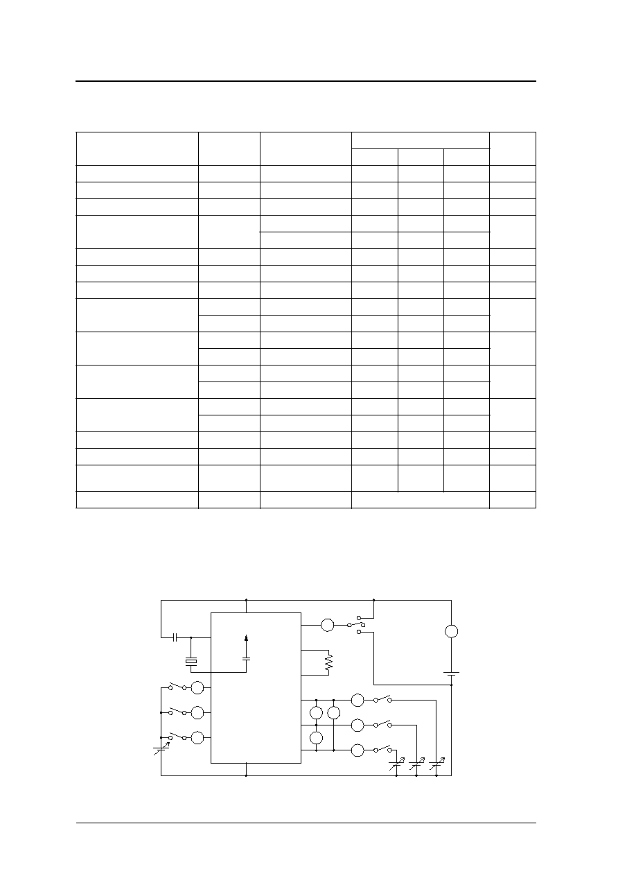
X'tal f
0
= 32.768kHz, C
I
= 35k
max, C
L
= 12.5pF, C
0
= 1.3pF, C
1
= 2.6pF, C
G
= 20pF, R
L
= 400
or 1k
XTN
O1
X'tal
O2
VDD
T1
C
G
XT
AO1
AI
C
D
I
AO
R
L
SN
SEL
AO2
AO3
VSS
I
O
A
A
A
A
A
A
A
I
O
V
O
A
I
DD
V
DD
A
A
A
V
I
I
I

CF5761 series
NIPPON PRECISION CIRCUITS INC.--6
FUNCTIONAL DESCRIPTION
Motor Output
The CF5761 series comprise devices with different step movement and sweep movement cycles and pulse-
widths.
Step movement
Sweep movement
Parameter
CF5761CA
CF5761EA
CF5761HA
CF5761LB
CF5761MB
CF5761NB
Active level
�
LOW
LOW
LOW
�
LOW
Movement cycle t
CY
[s]
0.0625
1
10
1
0.0625
1
Pulsewidth t
PW
[ms]
62.5
23.4
13.7
31.3
62.5
23.4
Movement
Sweep
Step
Step
Step
Sweep
Step
O1
VSS
O2
t
PW
VDD
VSS
VDD
t
CY
t
CY
t
PW
O1
t
CY
O2
t
CY
t
PW
VSS
VDD
VSS
VDD

CF5761 series
NIPPON PRECISION CIRCUITS INC.--7
Alarm Control
The alarm is controlled using AI, SN, and SEL inputs. These pins have built-in chattering elimination circuits
to prevent incorrect operation due to input chatter. The alarm output timing in response to these inputs is shown
in the following figure.
Input
Function
Input chatter elimination
AI
Alarm control input.
When AI is active, the specified alarm pattern is output on AO1, AO2 and AO3.
t
ON
< 62.5ms, the input is not accepted.
t
ON
> 125ms, the input is accepted.
62.5ms
t
ON
125ms, the input state is
undefined.
SN
Snooze function control input.
When the snooze input is accepted, the snooze time count begins. The snooze time is 300s.
SEL
Alarm function select input.
Selects one of two alarm patterns. When SEL is switched (from HIGH to LOW, or LOW to
HIGH), the snooze state and auto-stop function is released, and the alarm signal is output.
SEL
Alarm output
5min
5min
A
A
B
B A
SN
5min
B
5min 5min
AI
5min
5min
B
B
A
A
A
B
A
B
Auto-stop
released
Auto-stop
Snooze
released
Alarm
stops
ON
OFF
ON
OFF
B
A

CF5761 series
NIPPON PRECISION CIRCUITS INC.--8
Alarm Modes
The CF5761 series provide several alarm modes and various alarm pattern outputs for a wide range of clock
specifications, as described in the following table.
The alarm pattern timing for each device in the CF5761 series is shown in the series lineup.
The CF5761HA has a special modulated alarm pattern when SEL is HIGH, as shown in the following figure.
Outputs AO1 and AO3 have a frequency modulated alarm waveform output at the alarm fundamental fre-
quency of 4kHz (4096Hz). The modulation pattern is output on AO2.
Power-ON Initialization
The CF5761 series are reset to the following conditions after power is applied.
I
AI, SN, SEL input state
These inputs are reset to LOW, except where the device has an active-LOW input in which case it is reset to
HIGH. See the series lineup table.
I
O1, O2
In step movement devices, both outputs are HIGH and subsequent output occurs on O1. In sweep movement
devices, O1 is reset LOW and O2 is reset HIGH, and output starts immediately.
I
AO1, AO2, AO3
No output after reset. However, F output (CF5761EA: 32kHz on AO3) and clock output start immediately.
I
Test mode
Test mode is released after reset. Note that after the oscillator starts, the input state of each pin is read and
operation commences accordingly.
Alarm mode
Mode description
Output
Device
Simple alarm
A fixed alarm pattern is repeatedly rung (basic mode).
Motor bell
Piezo-electric speaker
Electromagnetic speaker
CF5761CA/EA/HA/LB/MB
Step tone
modulated alarm
At fixed intervals, the alarm pattern changes, increasing the tone pitch
with each step.
Motor bell
CF5761EA
Step volume
modulated alarm
At fixed intervals, using a fixed alarm pattern, the output waveform duty
changes, increasing the volume with each step.
Piezo-electric speaker
Electromagnetic speaker
CF5761LB/MB/NB
AO1 output
62.5msec 62.5msec
437.5msec
1sec
187.5msec
AO3 output
AO2 output
CF5761 series
NIPPON PRECISION CIRCUITS INC.--9
Test Function
The CF5761 series have a test mode of operation where the output cycles are compressed. T1 has a built-in
chattering elimination circuit to prevent incorrect operation due to input chatter. When T1 goes HIGH for an
interval of 31.25ms or greater, test mode is invoked. When T1 becomes open circuit, normal mode operation
resumes immediately and a 256Hz signal is output on T1.
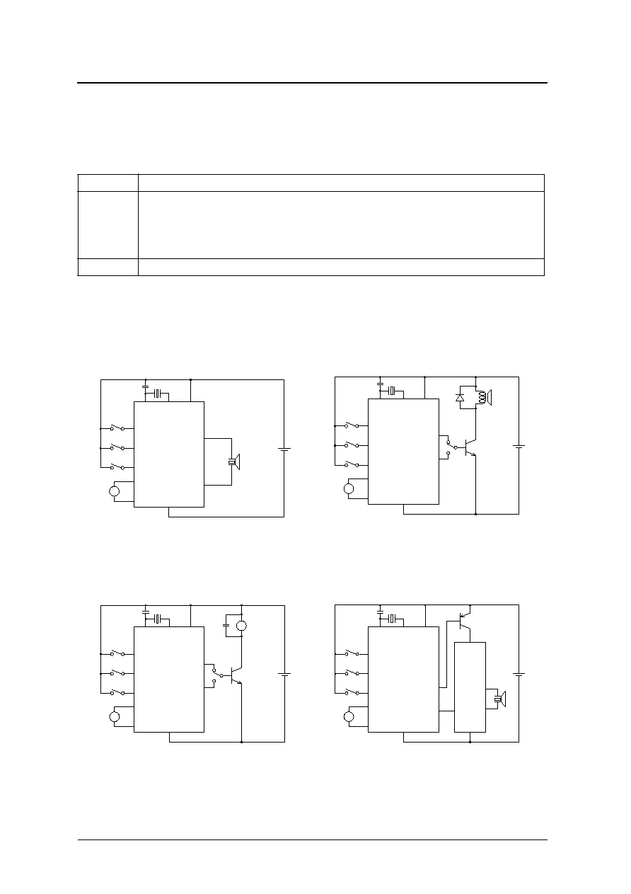
TYPICAL APPLICATION CIRCUITS
T1
Function
HIGH
Motor outputs: In step movement devices, the output runs 16 times faster with normal pulsewidth. In sweep movement devices,
the output runs 16 times faster with 50% duty pulsewidth.
Alarm outputs: Alarm operates at the same frequency with modulation frequency 16 times faster and step output changes 8 times
faster (CF5761EA, LB, NB) or 4 times faster (CF5761MB).
Snooze time, auto-stop time
1
: 281.25ms (CF5761EA, LB, NB) or 562.5ms (CF5761MB) in step output alarm mode, and
140.625ms in other modes.
1. The auto-stop time applies only to CF5761 versions that support the auto-stop function. See the series lineup table.
Open circuit
256Hz output (normal operation)
Piezo-electric speaker
Electromagnetic speaker
Motor bell
Melody alarm
XTN
X'tal
AO1
VDD
C
G
XT
AO2
AI
SN
SEL
AO3
VSS
O1
O2
M
XTN
X'tal
AO1
VDD
C
G
XT
AO2
AI
SN
SEL
AO3
VSS
O1
O2
M
XTN
X'tal
AO1
VDD
C
G
XT
AO2
AI
SN
SEL
AO3
VSS
O1
O2
M
M
Motorbell
XTN
X'tal
AO1
VDD
C
G
XT
AO2
AI
SN
SEL
AO3
VSS
O1
O2
M
VSS
F
VDD
Melody IC

CF5761 series
NIPPON PRECISION CIRCUITS INC.--10
NC0016AE
2001.12
NIPPON PRECISION CIRCUITS INC. reserves the right to make changes to the products described in this data sheet in order to
improve the design or performance and to supply the best possible products. Nippon Precision Circuits Inc. assumes no responsibility for
the use of any circuits shown in this data sheet, conveys no license under any patent or other rights, and makes no claim that the circuits
are free from patent infringement. Applications for any devices shown in this data sheet are for illustration only and Nippon Precision
Circuits Inc. makes no claim or warranty that such applications will be suitable for the use specified without further testing or modification.
The products described in this data sheet are not intended to use for the apparatus which influence human lives due to the failure or
malfunction of the products. Customers are requested to comply with applicable laws and regulations in effect now and hereinafter,
including compliance with export controls on the distribution or dissemination of the products. Customers shall not export, directly or
indirectly, any products without first obtaining required licenses and approvals from appropriate government agencies.
NIPPON PRECISION CIRCUITS INC.
4-3, Fukuzumi 2-chome, Koto-ku,
Tokyo 135-8430, Japan
Telephone: +81-3-3642-6661
Facsimile: +81-3-3642-6698
http://www.npc.co.jp/
Email: sales
@
npc.co.jp