01/03/28 ( 1 / 3 )
NJU7118
LOW POWER AND LOW OFFSET VOLTAGE
SUPER SMALL-SIZED SINGLE C-MOS COMPALATOR
!
GENERAL DESCRIPTION
!
PACKAGE INFORMATION
The
NJU7118
is a super small-sized package single
C-MOS comparators with open drain output.
The operating voltage is from 1V to 5.5V, and the interface
can be connected with most of TTL and C-MOS type standard
logic ICs.
Furthermore, The input offset voltage is lower than 4mV
and the package is super small-sized SC88A, therefore they
can be suitable for battery use items and other portable items.
!
FEATURES
!
PIN CONFIGURATION
"
Single Low Power Supply
V
DD
=1.0~5.5V
"
Low Offset Voltage
V
IO
=4mV max
"
Low Operating Current
I
DD
=10uA typ
"
Open Drain Output
"
Package Outline
SC88A
"
C-MOS Technology
!
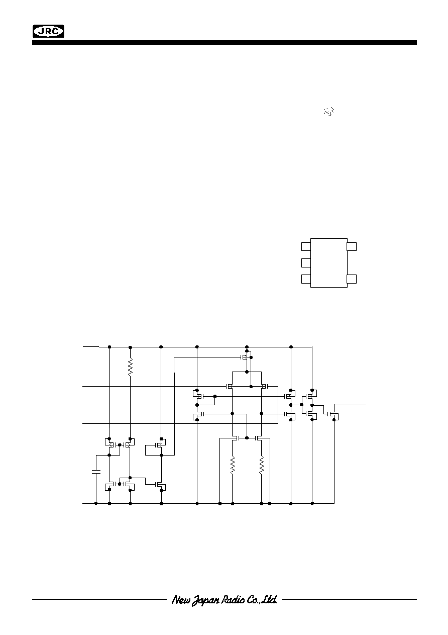
EQUIVALENT CIRCUIT
NJU7118F2
(Top View)
IN+
V
SS
IN-
V
DD
OUT
1
2
3 4
5
V
DD
IN-
OUT
IN+
V
SS
01/03/28 ( 2 / 3 )
NJU7118
!
ABSOLUTE MAXIMUM RATINGS
(Ta=25
�C)
PARAMETER SYMBOL
RATING
UNIT
Supply Voltage
V
DD
7.0 V
Differential Input Voltage
V
ID
�7.0 (Note1)
V
Common Mode Input Voltage
V
IC
-0.3~7.0 V
Power Dissipation
P
D
250 (Note2)
mW
Operating Temperature
Topr
-40~+85
�C
Storage Temperature
Tstg
-55~+125
�C
Note1) If the supply voltage (V
DD
) is less than 7.0V, the input voltage must not over the V
DD
level though 7.0V
is limit specified.
Note2) The power dissipation is value mounted on aglass epoxy board (FR-4) in size of 50x50x1.6 millimeters
square.
Note3) Decoupling capacitor should be connected between V
DD
and V
SS
due to the stabilized operation for the
circuit.
!
ELECTRICAL CHARACTERISTICS
(V
DD
=3.0V,R
L
=,Ta=25
�C)
PARAMETER SYMBOL CONDITIONS MIN
TYP
MAX
UNIT
Operating Voltage
V
DD
1.0 - 5.5
V
Input Offset Voltage
V
IO
V
IN
=V
DD
/2 -
-
4
mV
Input Offset Current
I
IO
- 1 -
pA
Input Bias Current
I
IB
- 1 -
pA
Input Common Mode
Voltage Range
V
ICM
0~2.5 -
-
V
Low Level Output Voltage
V
OL
I
OL
=+5mA -
-
0.3
V
Operating Current
I
DD
-
10
20 uA
(V
DD
=3.0V,f=10kHz,C
L
=15pF,Ta=25
�C)
PARAMETER SYMBOL CONDITIONS MIN
TYP
MAX
UNIT
Propagation Delay
Low to High
t
PLH
Over
Drive=100mV
- 540 - ns
Propagation Delay
High to Low
t
PHL
Over
Drive=100mV
- 190 - ns
Output Signal Falling Time
t
THL
Over
Drive=100mV - 4 -
ns
01/03/28 ( 3 / 3 )
NJU7118
!
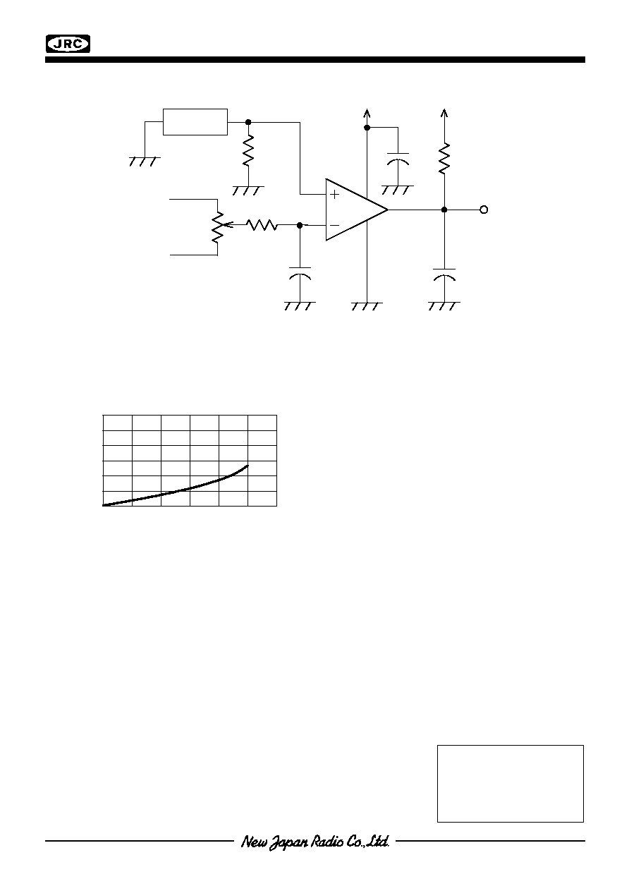
SWITCHING CHARACTERISTICS MEASUREMENT CIRCUIT
!
TYPICAL CHARACTERISTICS
Output Voltage vs. Output Current
(Sink)
0.0
0.5
1.0
1.5
2.0
2.5
3.0
0
5
10
15
20
25
30
Output Current IOL (mA)
OutputVoltage VOL (V)
[CAUTION]
The specifications on this data book are only
given for information , without any guarantee
as regards either mistakes or omissions.
The application circuits in this data book are
described only to show representative usages
of the product and not intended for the
guarantee or permission of any right including
the industrial rights.
1uF
5.1kohm
C
L
0.1uF
V
DD
10 Turn
0V
PULSE
GENERATER
50ohm
DUT
V
DD