 | –≠–ª–µ–∫—Ç—Ä–æ–Ω–Ω—ã–π –∫–æ–º–ø–æ–Ω–µ–Ω—Ç: NR8576AA | –°–∫–∞—á–∞—Ç—å:  PDF PDF  ZIP ZIP |

NR8576 Series
NIPPON PRECISION CIRCUITS--1
NIPPON PRECISION CIRCUITS INC.
Real-time Clock Modules
OVERVIEW
The NR8576 Series devices are serial-interface type
real-time clock module ICs with built-in crystal
oscillator elements. They feature timer counter cir-
cuits that keep track of time from the current second
to the current year, automatic leap-year adjustment,
and a supply voltage detect function. Also, a 32.768
kHz/1 Hz select output function is incorporated for
independent hardware control. They are available in
compact 14-pin SOPs (NR8576A
◊
) and miniature
18-pin SOPs (NR8576B
◊
).
FEATURES
s
Crystal oscillator element built-in for adjustment-
free use
s
Timer counters for second, minute, hour, day, day
of the week, month, and year
s
2.5 to 5.5 V operating voltage range
s
1.7 ± 0.3 V supply voltage detection threshold
s
1.0 µA at 3.0 V (typ) current consumption
s
Automatic leap-year calendar adjustment
s
32.768 kHz and 1 Hz output selectable
s
Package
∑ 14-pin SOP (NR8576A
◊
)
∑ 18-pin SOP (NR8576B
◊
)
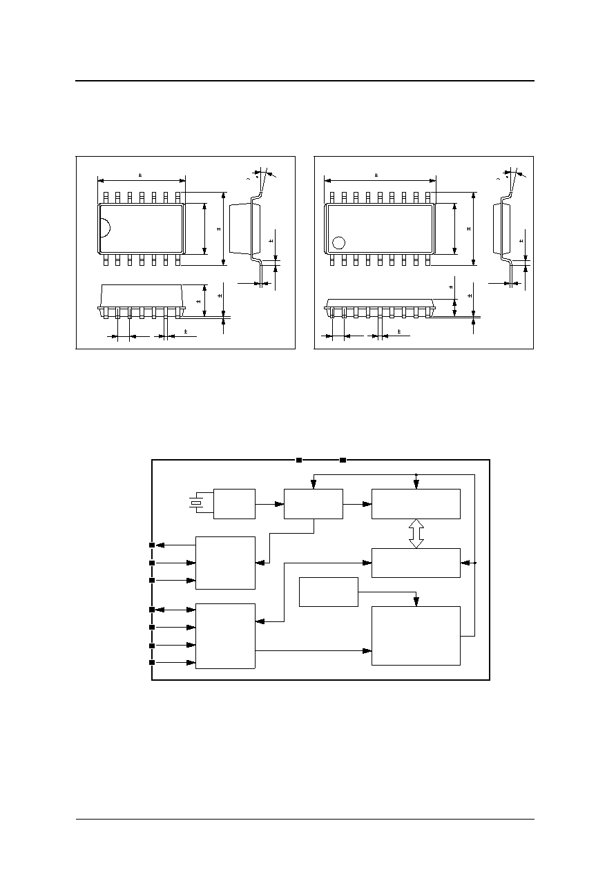
SERIES CONFIGURATION
PINOUTS
14-pin SOP
18-pin SOP
Device
Package
Frequency deviation
NR8576AA
14-pin SOP
5 ± 12 ppm
NR8576AB
14-pin SOP
5 ± 23 ppm
NR8576BA
18-pin SOP
5 ± 12 ppm
NR8576BB
18-pin SOP
5 ± 23 ppm
1
CE
2
N.C
3
VSS
4
N.C
5
N.C
6
FOUT
7
10
9
8
14
13
12
11
FSEL
WR
FOE
N.C
N.C
VDD
CLK
DATA
NR8576A
1
CE
2
N.C
3
VSS
4
N.C
5
N.C
6
FOUT
7
16
17
18
12
13
14
15
FSEL
WR
FOE
N.C
N.C
VDD
CLK
DATA
8
11
N.C
N.C
N.C
N.C
10
9
NR8576B
NR8576 Series
NIPPON PRECISION CIRCUITS--2
PACKAGE DIMENSIONS
Unit: mm
14-pin SOP
1.27
3.2 0.1
0.10 0.05
5.0
0 10
0.35 0.1
0.15
10.1 0.2
0.6 0.2
7.4 0.2
18-pin SOP
1.27
1.8 0.1
0.05 0.05
5.4
7.8 0.2
0 10
0.4 0.1
0.15
11.4 0.2
0.6 0.2
BLOCK DIAGRAM
OSC
Divider
Timer Counter
Shift Register
Voltage
Detect
I/O
Controller
Control
Circuit
VDD
VSS
DATA
CLK
CE
Output
Controller
FOUT
WR
FSEL
FOE
32.768kHz

NR8576 Series
NIPPON PRECISION CIRCUITS--3
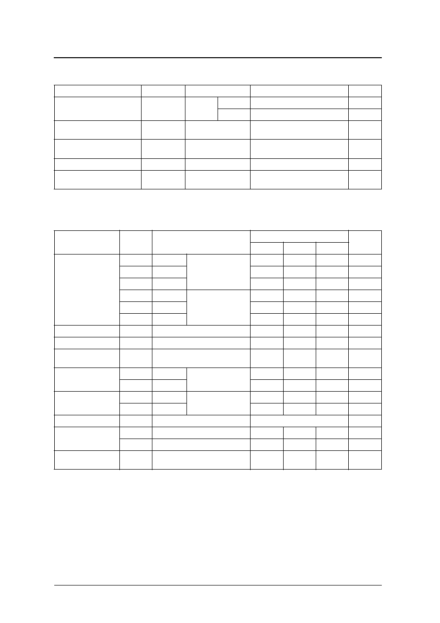
PIN DESCRIPTION
SPECIFICATIONS
Absolute Maximum Ratings
V
SS
= 0 V
Recommended Operating Conditions
V
SS
= 0 V
Name
I/O
Description
VSS
≠
Ground
CE
I
Chip enable.
HIGH: Enable
LOW: DATA goes high impedance; input on WR, CLK, and DATA stops; and the TM bit is cleared.
FSEL
I
FOUT output frequency select.
HIGH: 1 Hz
LOW: 32.768 kHz
WR
I
DATA input/output control switch.
HIGH: Data input mode (RTC write)
LOW: Data output mode (RTC read)
FOE
I
FOUT output enable control.
HIGH: The frequency selected by FSEL is output on FOUT.
LOW: FOUT goes high impedance.
VDD
≠
Supply voltage.
Connect a
0.1 µF capacitor between VDD and VSS.
CLK
I
System clock input.
Data is input (RTC write mode) and output (RTC read mode) on the rising edge of CLK.
DATA
I/O
Data read and write input/output
FOUT
O
Frequency output (output controlled by FOE and frequency selected by FSEL).
In 1 Hz output mode, the 1 Hz signal is synchronized to the internal 1 second signal.
FOUT output is not affected by the CE signal.
N. C
≠
No connection. Leave open for normal use.
Parameter
Symbol
Condition
Rating
Unit
Supply voltage range
V
DD
T
a
= 25
∞
C
-
0.3 to 7.0
V
Input voltage range
V
IN
T
a
= 25
∞
C
V
SS
-
0.3 to V
DD
+ 0.3
V
Output voltage range
V
OUT
T
a
= 25
∞
C
V
SS
-
0.3 to V
DD
+ 0.3
V
Storage temperature range
T
stg
-
55 to 125
∞
C
Soldering temperature
T
sld
260
∞
C
Soldering time
t
sld
10
s
Parameter
Symbol
Condition
Rating
Unit
Supply voltage range
V
DD
2.5 to 5.5
V
Clock supply voltage range
V
CLK
1.4 to 5.5
V
Operating temperature range
T
opr
-
40 to 85
∞
C
NR8576 Series
NIPPON PRECISION CIRCUITS--4
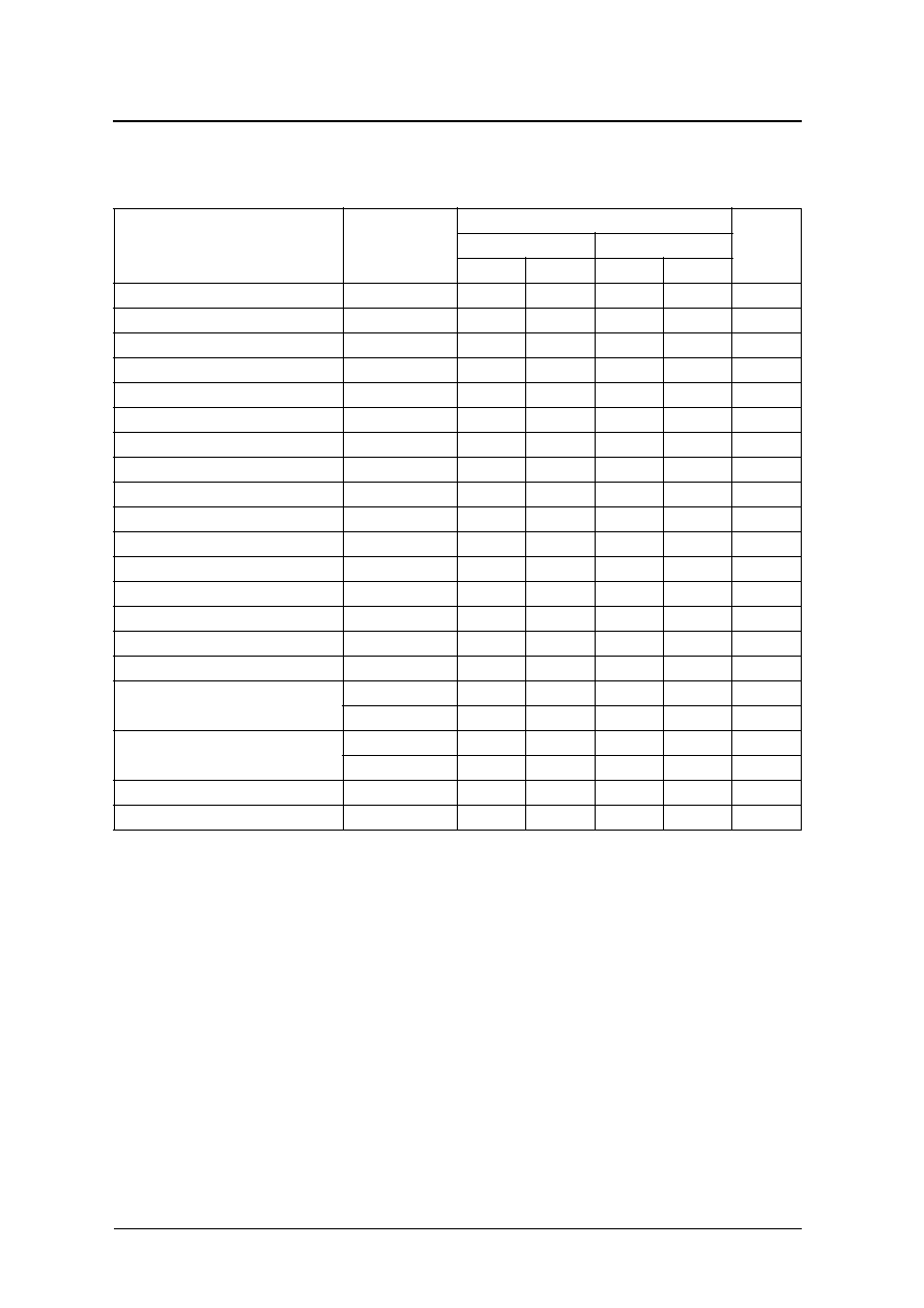
Oscillator Characteristics
DC Electrical Characteristics
V
SS
= 0 V, V
DD
= 5.0 V ± 10%, T
a
=
-
40 to 85
∞
C unless otherwise noted
Parameter
Symbol
Condition
Rating
Unit
Frequency deviation
f/f
O
T
a
= 25
∞
C,
V
DD
= 5.0 V
NR8576
◊
A
5 ± 12
ppm
NR8576
◊
B
5 ± 23
ppm
Frequency temperature characteristic
T
op
T
a
=
-
10 to 70
∞
C,
V
DD
= 5.0 V, 25
∞
C std
+10/
-
120
ppm
Frequency voltage characteristic
f/V
T
a
= 25
∞
C,
V
DD
= 2.0 to 5.5 V
±2
ppm/V
Oscillator start time
t
STA
T
a
= 25
∞
C, V
DD
= 2.5 V
3
s
Aging
f
A
T
a
= 25
∞
C, V
DD
= 5.0 V,
first year
±5
ppm
Parameter
Symbol
Condition
Rating
Unit
min
typ
max
Current consumption
I
DD1
V
DD
= 5.0 V
CE = V
SS
, FOE = V
SS
,
FSEL = V
DD
,
FOUT: floating
≠
1.5
3.0
µA
I
DD2
V
DD
= 3.0 V
≠
1.0
2.0
µA
I
DD3
V
DD
= 2.0 V
≠
0.5
1.0
µA
I
DD4
V
DD
= 5.0 V
CE = V
SS
, FOE = V
DD
,
FSEL = V
SS
,
FOUT: 32 kHz output
≠
4.0
10.0
µA
I
DD5
V
DD
= 3.0 V
≠
2.5
6.5
µA
I
DD6
V
DD
= 2.0 V
≠
1.5
4.0
µA
HIGH-level input voltage
V
IH
CE, FSEL, WR, FOE, CLK, DATA
0.8V
DD
≠
≠
V
LOW-level input voltage
V
IL
CE, FSEL, WR, FOE, CLK, DATA
≠
≠
0.2V
DD
V
Input OFF leakage current
I
OFF
CE, FSEL, WR, FOE, CLK;
V
IN
= V
DD
or V
SS
≠
≠
0.5
µA
HIGH-level output voltage
V
OH1
V
DD
= 5.0 V
I
OH
=
-
1.0 mA;
DATA, FOUT
4.5
≠
≠
V
V
OH2
V
DD
= 3.0 V
2.0
≠
≠
V
LOW-level output voltage
V
OL1
V
DD
= 5.0 V
I
OL
= 1.0 mA;
DATA, FOUT
≠
≠
0.5
V
V
OL2
V
DD
= 3.0 V
≠
≠
0.8
V
Output load fanout
N/C
L
FOUT
2 LSTTL/30 pF max.
Output leakage current
I
OZH
V
OUT
= 5.5 V; DATA, FOUT
-
1.0
≠
1.0
µA
I
OZL
V
OUT
= 0 V; DATA, FOUT
-
1.0
≠
1.0
µA
Supply voltage detect
threshold voltage
V
DT
1.4
1.7
2.0
V
NR8576 Series
NIPPON PRECISION CIRCUITS--5
AC Characteristics
V
DD
= 3.0 V, V
SS
= 0 V, T
a
= 25
∞
C unless otherwise noted
Parameter
Symbol
Rating
Unit
V
DD
= 5 V ± 10%
V
DD
= 3 V ± 10%
min
max
min
max
CLK clock period
t
CLK
0.75
7800
1.5
7800
µs
CLK LOW-level pulsewidth
t
CLKL
0.375
3900
0.75
3900
µs
CLK HIGH-level pulsewidth
t
CLKH
0.375
3900
0.75
3900
µs
CE setup time
t
CES
0.375
3900
0.75
3900
µs
CE hold time
t
CEH
0.375
≠
0.75
≠
µs
CE enable time
t
CE
≠
0.9
≠
0.9
s
Write data setup time
t
SD
0.1
≠
0.2
≠
µs
Write data hold time
t
HD
0.1
≠
0.1
≠
µs
WR setup time
t
WRS
100
≠
100
≠
ns
WR hold time
t
WRH
100
≠
100
≠
ns
DATA output delay time
t
DATD
≠
0.2
≠
0.4
µs
DATA output floating time
t
DZ
≠
0.1
≠
0.2
µs
Clock rise time
t
r1
≠
50
≠
100
ns
Clock fall time
t
f1
≠
50
≠
100
ns
FOUT rise time (C
L
= 30 pF)
t
r2
≠
100
≠
200
ns
FOUT fall time (C
L
= 30 pF)
t
f2
≠
100
≠
200
ns
Disable time (C
L
= 30 pF)
t
HZ
≠
100
≠
200
ns
t
LZ
≠
100
≠
200
ns
Enable time (C
L
= 30 pF)
t
ZH
≠
100
≠
200
ns
t
ZL
≠
100
≠
200
ns
FOUT duty cycle (C
L
= 30 pF)
Duty
40
60
40
60
%
Wait time
t
RCV
0.95
≠
1.9
≠
µs

NR8576 Series
NIPPON PRECISION CIRCUITS--6
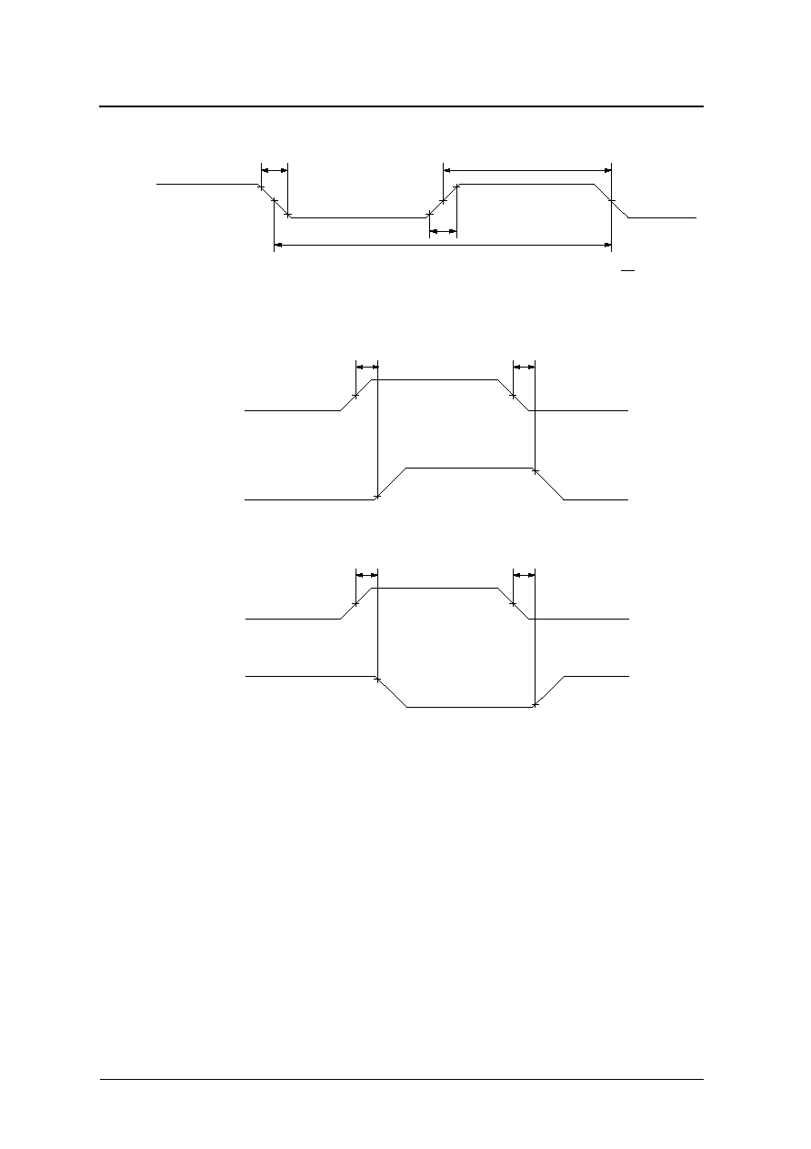
Timing Diagrams
Data read
Data write
WR
CE
CLK
DATA
t
CE
t
WRS
t
CES
t
CLKH
t
CLK
t
DATD
t
CLKL
t
f1
t
r1
t
DZ
t
CEH
t
RCV
t
WRH
WR
CE
CLK
DATA
t
CE
t
WRS
t
CES
t
CLKH
t
CLK
t
SD
t
CLKL
t
f1
t
r1
t
CEH
t
RCV
t
WRH
t
HD
NR8576 Series
NIPPON PRECISION CIRCUITS--7
FOUT
Disable/Enable
Note that FOE and FSEL do not have chatter elimination circuits. Consequently, switching either FOE or
FSEL during 32 kHz mode operation may generate chatter noise on the FOUT output. Also, note that the 1 Hz
and 32 kHz oscillators are not synchronized to each other, so switching intervals shortens the duty cycle.
Accordingly, a wait time (
chattering time + output frequency period) should be incorporated when switching
intervals.
FOUT
t
r2
t
H
t
t
f2
10%
50%
90%
Duty=
X
100(%)
t
t
H
FOE
t
HZ
t
ZH
10%
50%
90%
50%
FOUT
FOE
t
LZ
t
ZL
10%
50%
90%
50%
FOUT
NR8576 Series
NIPPON PRECISION CIRCUITS--8
FUNCTIONAL DESCRIPTION
Timer data configuration
s
Counter data in BCD code format
s
Automatic long/short month and leap-year adjustment
s
24-hour time display
s
LSB first write and read data
1. * bit: Optional write bits.
2. FDT bit: Supply voltage detect bit
∑ The FDT bit is set to 1 when the voltage between VDD and VSS falls below 1.7 ± 0.3 V.
∑ The FDT bit is reset to 0 for data reads longer than 48 bits. Note that the FDT bit is not reset to 0 for data
reads of 47 bits or less.
∑ The read/write data bits should be should be set to 0. After the supply voltage is applied, the FDT bit
should be set to 0.
3. TM bit: Factory test bit. Should be set to 0 for normal use.
FDT
S40
S20
S10
S8
S1
S2
S4
mi40
mi20
mi10
mi8
mi1
mi2
mi4
h20
h10
h8
h1
h2
h4
w1
w2
w4
d20
d10
d8
d1
d2
d4
mo10
mo8
mo1
mo2
mo4
TM
y80
y40
y20
y10
y8
y1
y2
y4
MSB
LSB
Second ( 0 to 59 )
Minute ( 0 to 59 )
Hour ( 0 to 23 )
Week ( 1 to 7 )
Day ( 1 to 31 )
Month ( 1 to 12 )
Year ( 0 to 99 )
VDD
CE
V
DET
FDT
(READ MODE)
Detected Pulse
0.5 second
0.5 second
NR8576 Series
NIPPON PRECISION CIRCUITS--9
Data Read
Data is output when WR is LOW and CE is HIGH.
Time and calendar data is loaded into shift registers
on the first rising edge of the clock CLK, and the sec-
onds' digit LSB is output on DATA.
The data is then loaded and shifted in the sequence
second, minute, hour, week, day, and month on the
rising edge of CLK, and output on DATA. The output
data is valid after 52 rising edges of the clock; data
input after 52 cycles does not alter the first 52 bits of
valid data.
WR
CE
CLK
DATA
S1
second
year
FDT
S40
S20
S10
S8
S4
S2
y80
y40
y20
y10
y8
1
2
3
52
53
54
54+n
OUTPUT MODE
NON CHANGE
OUTPUT DATA
Within the 52 cycles of valid data, data already input
can be output if there is a falling edge of CE after the
corresponding number of cycles. For example, the
data comprising the second-to-week is output is CE
goes LOW after 28 clock cycles.
For continuous data reads, a wait time (t
RCV
) is
required before the next data cycle if CE has gone
LOW.
Note that if an update operation (a 1 s carry) occurs
during a data read, an error of
-
1 s in the read data is
generated.
The data read time should be completed after
t
CE
0.9 s.

NR8576 Series
NIPPON PRECISION CIRCUITS--10
NIPPON PRECISION CIRCUITS INC. reserves the right to make changes to the products described in this data sheet in order to
improve the design or performance and to supply the best possible products. Nippon Precision Circuits Inc. assumes no responsibility for
the use of any circuits shown in this data sheet, conveys no license under any patent or other rights, and makes no claim that the circuits
are free from patent infringement. Applications for any devices shown in this data sheet are for illustration only and Nippon Precision
Circuits Inc. makes no claim or warranty that such applications will be suitable for the use specified without further testing or modification.
The products described in this data sheet are not intended to use for the apparatus which influence human lives due to the failure or
malfunction of the products. Customers are requested to comply with applicable laws and regulations in effect now and hereinafter,
including compliance with export controls on the distribution or dissemination of the products. Customers shall not export, directly or
indirectly, any products without first obtaining required licenses and approvals from appropriate government agencies.
NIPPON PRECISION CIRCUITS INC.
4-3, Fukuzumi 2-chome
Koto-ku, Tokyo 135-8430, Japan
Telephone: 03-3642-6661
Facsimile: 03-3642-6698
NC9603CE
1997.06
NIPPON PRECISION CIRCUITS INC.
Data Write
Data is input when WR is HIGH and CE is HIGH.
The seconds' digit signal to the timer counter stops
on the first falling edge of CLK and the counter
remains stopped until the next rising edge of CE. The
1 Hz to 128 Hz frequency divider step counters are
reset during the interval between the first and second
rising edges of CLK.
The data is then input on DATA into the shift regis-
ter, starting with seconds' digit LSB synchronized
with the rising edge of CLK.
After the final data is input into the shift register fol-
lowing 52 cycles, the shift register contents are trans-
WR
CE
CLK
DATA
S1
second
year
FDT
S40
S20
S10
S8
S4
S2
y80
y40
y20
y10
y8
1
2
3
52
53
54
54+n
INPUT MODE
ferred to the timer counters. Note that a data write
must contain 52 bits of input data. If CE goes LOW
before 52 bits are input, the input data is invalid. If
the input data exceeds 52 bits, data from the 53rd bit
is ignored (the first 52 bits remain valid).
The data write time should be completed after
t
CE
0.9 s.
If a data read occurs immediately after a data write, a
wait time (t
RCV
) is required if CE has gone LOW.
Note that writing null data will cause incorrect oper-
ation. All bits must be valid data bits.