QS7777PF/CF
NIPPON PRECISION CIRCUITS--1
NIPPON PRECISION CIRCUITS INC.
QSurroundTM 3D Virtual Audio Processor
for Dolby AC-3 and ProLogic
OVERVIEW
The QS7777PF/CF is an audio processor IC which
implements the QSurroundTM technology developed
and licensed by QSound Labs, Inc. It processes
Dolby Digital (AC-3) and Dolby Surround audio sig-
nals to produce enhanced virtual 3D sounds, even for
2-speaker systems. It can generate 2, 3, 4, and 5-
channel speaker configurations, all with enhanced
surround signal outputs.
FEATURES
s
Enhanced surround signal from Dolby Digital
(AC-3) and Dolby Surround (ProLogic) input sig-
nals
s
2-step adjustable sound enhancement
s
Supported speaker configurations
� Dolby Digital (AC-3) 6-channel signals to 2, 3,
4, 5-channel speaker QSurround signal configu-
rations
� Dolby Surround (ProLogic) 4-channel signals
to 2, 3, 4-channel speaker QSurround signal
configurations
s
Monaural to virtual stereo conversion
s
Parallel and 2 serial interface control modes
selectable
� QS7777CF: I
2
C bus 2-wire serial interface
1
� QS7777PF: 3-wire serial interface (Data, Clock,
Strobe)
s
5 to 13V analog supply
s
4.5 to 5.5V digital supply
s
48-pin QFP package
1. NPC employs I
2
C bus serial interface components
under license from Philips, and conforms to the Phil-
ips I
2
C bus specifications.
APPLICATIONS
s
DVD and laser disk players
s
TV and AV equipment
s
Multimedia products (including sound cards)
s
Car audio
ORDERING INFORMATION
PINOUT
QS7777PF
QS7777CF
I
2
C bus is a registered tra d e m a r k of Philips Electronics N.V.
Dolby and the double-D symbol are registered tra d e m a r ks of Dolby Laboratories Licensing Corporation.
D e vice
P a ck ag e
Q S 7 7 7 7 P F
48-pin QFP
Q S 7 7 7 7 C F
48-pin QFP
Top view
Top view
38
39
40
41
42
43
44
45
46
47
48
1
2
3
4
5
6
7
8
9
10
11
13
14
15
16
17
18
19
20
21
22
23
26
27
28
29
30
31
32
33
34
35
36
QXDC3
QXDC4
FLIN
FRIN
CIN
SUBIN
RLIN
RRIN
MSC4
MSC5
MSC6
QXAC3
QXAC2
QXAC1
FLOUT
FROUT
COUT
RLOUT
RROUT
VDD
P/S
BYP
VREFOUT
VREFIN
MSC3
MSC2
MSC1
GND
PSAVE(STRB)
MUTE(SCL)
SPREAD(SDA)
AC
AR
QXDC1
QXCC4
QXCC3
QXCC2
QXCC1
VCC
QXBC5
QXBC4
QXBC3
QXBC2
QXBC1
12
MO
24
QXAC4
37
QXDC2
25
QXAC5
QS7777PF
38
39
40
41
42
43
44
45
46
47
48
1
2
3
4
5
6
7
8
9
10
11
13
14
15
16
17
18
19
20
21
22
23
26
27
28
29
30
31
32
33
34
35
36
QXDC3
QXDC4
FLIN
FRIN
CIN
SUBIN
RLIN
RRIN
MSC4
MSC5
MSC6
QXAC3
QXAC2
QXAC1
FLOUT
FROUT
COUT
RLOUT
RROUT
VDD
P/S
BYP
VREFOUT
VREFIN
MSC3
MSC2
MSC1
GND
PSAVE
MUTE(SCL)
SPREAD(SDA)
AC
AR
QXDC1
QXCC4
QXCC3
QXCC2
QXCC1
VCC
QXBC5
QXBC4
QXBC3
QXBC2
QXBC1
12
MO
24
QXAC4
37
QXDC2
25
QXAC5
QS7777CF
QS7777PF/CF
NIPPON PRECISION CIRCUITS--2
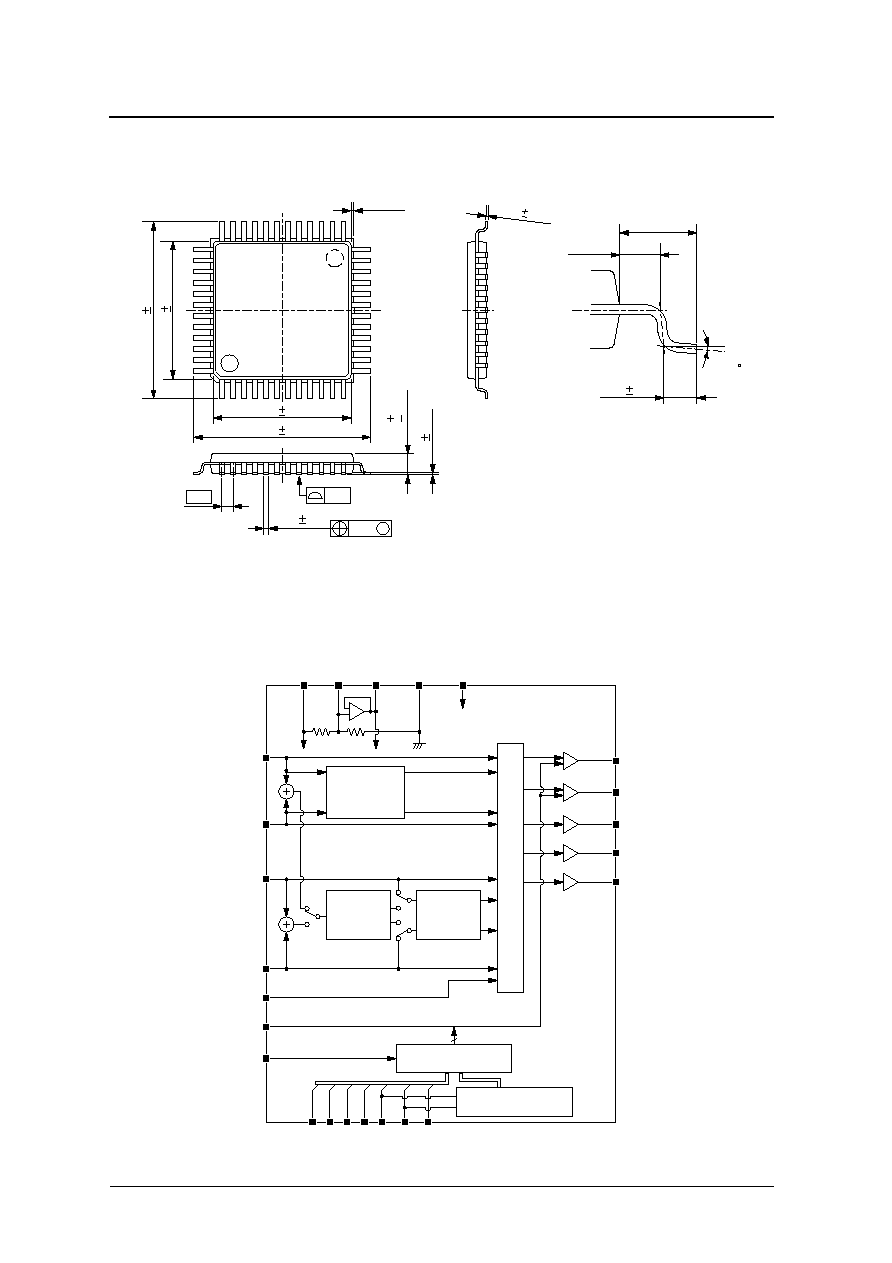
PACKAGE DIMENSIONS
Unit: mm
BLOCK DIAGRAM
0.19 0.05
0.10
0.07
0.10
0.17 0.05
0 to 10
1.50
0.10
0.20
0.08
M
0.50
0.35max
1.00typ
7.00 0.20
9.00 0.20
7.00
0.20
9.00
0.20
0.50 0.10
0.339typ
RROUT
VREFOUT
GND
VREFIN
VCC
FLIN
FRIN
RLIN
FLOUT
PSAVE
(STRB)
VDD
Digital
Circuitry
Analog
Circuitry
VREF
Qsound
3D Process
MONO to
STEREO
Qsound
3D Process
CIN
SUBIN
P/S
M
M
FROUT
RLOUT
RROUT
COUT
Decoder/Data Latches
Controls
Parallel/Serial Switch
,,,,,,
,,,,,,
,,,,,,
DATA
CLK
Shift
Register
MUTE
(SCL)
SPREAD
(SDA)
AC
AR
MO
BYP
,,,,,,,,,,,,,,,,,
,,,,,,,,,,,,,,,,,
,,,,,,,,,,,,,,,,,
Matrix Switch
QS7777PF/CF
NIPPON PRECISION CIRCUITS--3
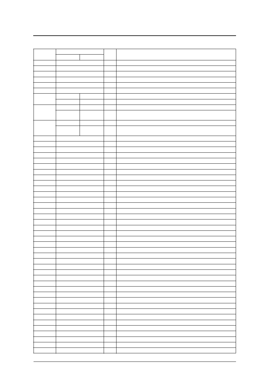
PIN DESCRIPTION
N u m b e r
N a m e
I/O
Description
P arallel
Serial
1
V R E F O U T
O
V
C C
/2 reference voltage output
2
V R E F I N
I
V
C C
/2 reference voltage input (biased internally to V
C C
/2)
3
M S C 3
I
Mono/stereo conversion filter capacitor 3
4
M S C 2
I
Mono/stereo conversion filter capacitor 2
5
M S C 1
I
Mono/stereo conversion filter capacitor 1
6
G N D
�
G r o u n d
7
P S AV E
�
I
P ow er save control (HIGH: pow er save on, LOW : pow er save off)
�
S T R B
I
Ser ial data strobe (not used on I
2
C bus device QS7777CF)
8
M U T E
�
I
Mute signal control (HIGH: mute on, LOW : mute off)
�
S C L
I
Ser ial data shift clock input (QS7777CF: CMOS input, no protection diode connected
between this pin and V D D )
9
S P R E A D
�
I
Enhancement control (HIGH: m a x i mum spread, LOW : minimum spread)
�
S D A
I/O
Ser ial data input (and ACK signal output for I
2
C bus device QS7777CF: n-channel
open-drain pin, no protection diode connected between this pin and V D D ) .
1 0
A C
I
Center speaker control (HIGH: actual center, LOW : virtual center)
1 1
A R
I
Rear speaker control (HIGH: actual rear, LOW : virtual rear)
1 2
M O
I
Mono-to-stereo conver t select (HIGH: ON, LOW : OFF)
1 3
B Y P
I
Bypass/QSurround select control (HIGH: bypass, LOW : QSurround)
1 4
P / S
I
Interface method select (HIGH: parallel input, LOW : serial input)
1 5
V D D
�
4.5 to 5.5V DC digital supply
1 6
R R O U T
O
Rear right-channel signal output
1 7
R L O U T
O
Rear left-channel signal output
1 8
C O U T
O
Center signal output
1 9
F R O U T
O
Front right-channel signal output
2 0
F L O U T
O
Front left-channel signal output
2 1
Q X A C 1
I
QExpander fi lter A capacitor 1
2 2
Q X A C 2
I
QExpander fi lter A capacitor 2
2 3
Q X A C 3
I
QExpander fi lter A capacitor 3
2 4
Q X A C 4
I
QExpander fi lter A capacitor 4
2 5
Q X A C 5
I
QExpander fi lter B capacitor 5
2 6
Q X B C 1
I
QExpander fi lter B capacitor 1
2 7
Q X B C 2
I
QExpander fi lter B capacitor 2
2 8
Q X B C 3
I
QExpander fi lter B capacitor 3
2 9
Q X B C 4
I
QExpander fi lter B capacitor 4
3 0
Q X B C 5
I
QExpander fi lter B capacitor 5
3 1
V C C
�
5 to 13V DC analog supply
3 2
Q X C C 1
I
QExpander fi lter C capacitor 1
3 3
Q X C C 2
I
QExpander fi lter C capacitor 2
3 4
Q X C C 3
I
QExpander fi lter C capacitor 3
3 5
Q X C C 4
I
QExpander fi lter C capacitor 4
3 6
Q X D C 1
I
QExpander fi lter D capacitor 1
3 7
Q X D C 2
I
QExpander fi lter D capacitor 2
3 8
Q X D C 3
I
QExpander fi lter D capacitor 3
3 9
Q X D C 4
I
QExpander fi lter D capacitor 4
4 0
F L I N
I
Front left-channel signal input
4 1
F R I N
I
Front right-channel signal input
4 2
C I N
I
Center-channel signal input
4 3
S U B I N
I
S u b - w oofer signal input
4 4
R L I N
I
Rear left-channel signal input
4 5
R R I N
I
Rear right-channel signal input
4 6
M S C 4
I
Mono/stereo conversion filter capacitor 4
4 7
M S C 5
I
Mono/stereo conversion filter capacitor 5
4 8
M S C 6
I
Mono/stereo conversion filter capacitor 6

QS7777PF/CF
NIPPON PRECISION CIRCUITS--4
SPECIFICATIONS
Absolute Maximum Ratings
Recommended Operating Conditions
DC Characteristics
V
CC
= 9V, V
DD
= 5V, T
a
= 25
�
C
P arameter
S y m b o l
Rating
Unit
Supply voltage range (analog)
V
C C
-
0.3 to 15
V
Supply voltage range (digital)
V
D D
-
0.3 to 7
V
Input voltage range (analog)
V
I A N A
-
0.3 to V
C C
+ 0.3
V
Input voltage range (digital)
V
IDIG
-
0.3 to V
D D
+ 0.3
V
I
2
C signal input voltage (SDA, SCL)
V
I O P E N
1 0
V
P ow er dissipation
P
D
2 5 0
m W
Storage temperature ra n g e
T
stg
-
40 to 125
�
C
Soldering temperature
T
sld
2 5 5
�
C
Soldering time
t
sld
1 0
s
P arameter
S y m b o l
Rating
Unit
Supply voltage range (analog)
V
C C
5 to 13
V
Supply voltage range (digital)
V
D D
4.5 to 5.5
V
O p e rating temperature ra n g e
T
opr
-
20 to 70
�
C
P arameter
S y m b o l
Condition
Rating
Unit
m i n
typ
m a x
Analog input impedance
Z
A I N
FLIN, FRIN, RLIN, RRIN, CIN, COUT
1 6
2 0
2 4
k
Reference voltage output
V
R E F O U T
�
V
C C
/2
�
V
HIGH-level input voltage
V
IH
0.7V
D D
�
�
V
L O W -level input voltage
V
IL
�
�
0.3V
D D
V
Input leakage current
I
L E A K
-
3
�
3
� A
Input leakage current (I
2
C input)
I
L O P E N
S D A, SCL, 10V input voltage
-
3
�
3
� A
L O W -level output voltage
V
O L
A CK signal output on SDA, 3mA sink
current
0
�
0.4
V
Supply voltage (analog)
V
C C
5
�
1 3
V
Supply voltage (digital)
V
D D
4.5
�
5.5
V
Current consumption (analog)
I
C C
Quiescent input signal
�
1 0
1 3
m A
Current consumption (digital)
I
D D
�
0.3
0.5
m A
Standby current (analog)
I
C C S A V E
�
0.1
0.2
m A

QS7777PF/CF
NIPPON PRECISION CIRCUITS--5
Noise and THD Characteristics
V
CC
= 9V, V
DD
= 5V, T
a
= 25
�
C
AC Characteristics
V
CC
= 9V, V
DD
= 5V, T
a
= 25
�
C
P arameter
S y m b o l
Condition
Rating
Unit
m i n
typ
m a x
Bypass noise voltage
N
B Y P
BYP = AR = AC = HIGH, MO = SPREAD =
L O W , "A"-wgt, FLOUT, R L O U T, FRO U T,
R R O U T, C O U T
�
1 1
2 2
� V
R M S
QSurround noise voltage (front)
N
Q S F
B Y P = M O = S P R E A D = L OW , AR = AC =
HIGH, "A"-wgt, FLOUT, FRO U T
�
1 6
3 2
� V
R M S
QSurround noise voltage (rear)
N
Q S R
B Y P = M O = S P R E A D = L OW , AR = AC =
HIGH, "A"-wgt, RLOUT, RRO U T
�
1 4
2 8
� V
R M S
QSurround mono total har monic
distortion (front)
T H D
F
MO = HIGH, all other excluding MO =
L O W , all inputs 1V
R M S
, f = 1kHz, FRO U T,
F L O U T
�
�
0.1
%
QSurround mono total har monic
distortion (rear)
T H D
R
MO = AR = AC = HIGH, BYP = SPREAD =
A E = L OW , all inputs 1V
R M S
, f = 1kHz,
R R O U T, R L O U T, C O U T
�
�
0.1
%
P arameter
S y m b o l
Condition
Rating
Unit
m i n
typ
m a x
Front maximum input voltage 1
V
F I N 1
FLIN = FRIN, RLIN = RRIN = CIN = SUBIN
= 0V, BYP = LOW , f = 1kHz
1.4
�
�
V
R M S
Front maximum input voltage 2
V
F I N 2
FLIN =
-
FRIN, RLIN = RRIN = CIN =
S U B I N = 0 V, BYP = LOW , f = 1kHz
0.5
�
�
V
R M S
R e a r m a x i mum input voltage 1
V
R I N 1
RLIN = RRIN, FLIN = FRIN = CIN = SUBIN
= 0V, BYP = LOW , AR = LOW , f = 1kHz
1.4
�
�
V
R M S
R e a r m a x i mum input voltage 2
V
R I N 2
RLIN =
-
RRIN, FLIN = FRIN = CIN =
S U B I N = 0 V, BYP = LOW , AR = LOW ,
f = 1kHz
0.3
�
�
V
R M S
Center maximum input voltage
V
C I N
FLIN = FRIN = RLIN = RRIN = SUBIN =
0 V, BYP = LOW , AC = LOW , f = 1kHz
1.7
�
�
V
R M S
S u b - w oofer maximum input voltage
V
S U B I N
FLIN = FRIN = RLIN = RRIN = CIN = 0V,
f = 1kHz
2.2
�
�
V
R M S
FIN to FOUT bypass gain
G
F F B Y P
BYP = HIGH, f = 1kHz, FLIN to FLOUT,
FRIN to FRO U T
-
2
0
2
d B
RIN to RO U T b ypass gain
G
R R B Y P
BYP = HIGH, AR = HIGH, f = 1kHz,
R L I N t o R L O U T, RRIN to RRO U T
-
2
0
2
d B
RIN to FOUT bypass gain
G
R F B Y P
BYP = HIGH, AR = LOW , f = 1kHz,
RLIN to FLOUT, RRIN to FRO U T
-
2
0
2
d B
CIN to COUT gain
G
C C
A C = HIGH, f = 1kHz, CIN to COUT
-
2
0
2
d B
CIN to FOUT gain
G
C F
A C = LOW , f = 1kHz, CIN to FLOUT,
CIN to FRO U T
-
2.8
-
0.8
1.2
d B
SUBIN to FOUT gain
G
S U B F
f = 1kHz, SUBIN to FLOUT, SUBIN to
F R O U T
-
8
-
6
-
4
d B
FIN to FOUT gain
G
F F
S P R E A D = H I G H , B Y P = L OW , f = 1kHz,
FLIN to FLOUT, FRIN to FRO U T
5.7
7.5
9.5
d B
FIN to FOUT crosstalk gain
G
F X F
S P R E A D = H I G H , B Y P = L OW , f = 1kHz,
FLIN to FRO U T, FRIN to FLOUT
3.7
5.7
7.7
d B
RIN to ROUT gain
G
R R
B Y P = L OW , AR = HIGH, f = 1kHz,
R L I N t o R L O U T, RRIN to RRO U T
2.7
4.7
6.7
d B
RIN to ROUT crosstalk gain
G
R X R
B Y P = L OW , AR = HIGH, f = 1kHz,
RLIN to RRO U T, RRIN to RLOUT
-
1.2
0.8
2.8
d B