 | –≠–ª–µ–∫—Ç—Ä–æ–Ω–Ω—ã–π –∫–æ–º–ø–æ–Ω–µ–Ω—Ç: SC47374S | –°–∫–∞—á–∞—Ç—å:  PDF PDF  ZIP ZIP |
SM9103M
NIPPON PRECISION CIRCUITS--1
NIPPON PRECISION CIRCUITS INC.
DVDRAM Head Amplifier LSI
OVERVIEW
The SM9103M is a photodiode photoelectric cur-
rent-to-voltage conversion head amplifier LSI for
optical disk pickups in DVDRAM/DVDROM equip-
ment. It sums the photodiode current data signals and
then converts the signals to a differential signal for
output. The output tracking servo and focusing servo
signals are derived from built-in sum and difference
circuits, and the gain for these servo signals can be
adjusted using serial interface controls. Each of the
signals from the photodiodes, used to generate DPD
(Differential Phase Detection) tracking servo signal,
is current-to-voltage converted and then also output.
It operates from a single 5 V supply, and is available
in 36-pin plastic SSOP packages.
FEATURES
s
RAM/ROM gain switching, low-noise RF signal
generator (differential output)
s
ROM tracking DPD signal output
s
Variable-gain RAM tracking push-pull signal out-
put
s
Address signal, high-speed push-pull signal output
s
Variable-gain focus error signal output
s
Tracking PD sum signal output
s
Focus PD sum signal output
s
Offset correction timing output (logic)
s
Temperature monitor function
s
Serial interface to control internal parameter set-
tings
s
Sleep-mode function
s
Single 5 V supply
s
36-pin plastic SSOP
TYPICAL APPLICATIONS
s
Double-speed DVDROM equipment
s
Double-speed DVDRAM equipment
ORDERING INFORMATION
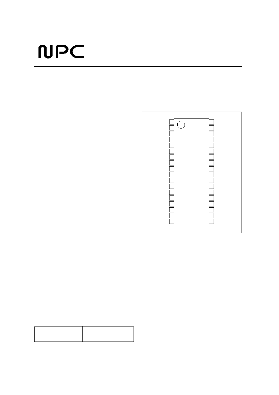
PINOUT
36-pin SSOP
(Top view)
Device
Package
SM9103M
36-pin SSOP
1
MODE
2
WRITE
3
DGND
4
DVCC
5
TEMPO
6
TEMPI
7
T1
8
T2
9
T3
10
T4
11
F1
12
F2
13
AGND
14
VREF
15
FSUBB
16
FSUB
17
FADDB
18
FADD
19
AGND
20
AVCC
21
DPDD
22
DPDC
23
DPDB
24
DPDA
25
DATAN
26
DATAP
27
TSUBB
28
TSUB
29
CAPAN
30
CAPAP
31
TADDB
32
TADD
33
CALREQ
34
SENB
35
SDATA
36
SCLK
SM9103M
NPC

SM9103M
NIPPON PRECISION CIRCUITS--2
PACKAGE DIMENSIONS
(Unit: mm)
BLOCK DIAGRAM
2.44 to 2.64
0.85
15.20 to 15.40
7.40 to 7.60
0.29 to 0.39
0.80
0.10 to 0.30
0.51 to 1.01
10.11 to 10.51
0.63 ± 0.10
7∞
0 to 8∞
0.23 to 0.32
7∞
0.51
±
0.20
45∞
R0.63 to 0.89
A
B
C
D
A+B+C+D
(A+B)-(C+D)
DATAP
DATAN
TADDB
TADD
CAPAP
CAPAN
TSUBB
TSUB
DPDA
DPDB
DPDC
DPDD
CALREQ
FSUB
FSUBB
FADDB
FADD
F2
F1
AGND
AVCC
TEMPO
TEMPI
T4
T3
T2
T1
WRITE
MODE
SDATA
SENB
SCLK
VREF
to each block
Serial interface
Gain switching
amplifier
(RAM read/write,
ROM read)
Analog
Signal
processor
Offset canceller
Thermal sensor
Canceller control
Offset canceller
Gain switching
amplifier
Differential
output buffer
Amplifier
Gain switch
(2dB step)
Buffer
Buffer
Buffer
Buffer
Differential
output buffer
Gain switch
(2dB step)
Amplifier
Analog
Signal
processor
+5V
+5V
DGND
DVCC

SM9103M
NIPPON PRECISION CIRCUITS--3
PIN DESCRIPTION
Number
Name
I/O
1
1. I = input, Ipd = Input with built-in pull-down resistor, I/O = input/output, O = output
Function
1
MODE
Ipd
Mode switching/offset correction control input 1
2
WRITE
Ipd
Mode switching/offset correction control input 2
3
DGND
≠
Logic circuit ground. Connect to the analog ground if there is no dedicated pickup or logic ground.
4
DVCC
≠
Logic circuit supply. Connect to the analog supply if there is no dedicated pickup or logic supply.
5
TEMPO
O
Thermal sensor test output. Leave open for normal operation
6
TEMPI
I
Thermal sensor test input. Leave open for normal operation
7
T1
I
Tracking PD input A
8
T2
I
Tracking PD input B
9
T3
I
Tracking PD input C
10
T4
I
Tracking PD input D
11
F1
I
Focus PD input E
12
F2
I
Focus PD input F
13
AGND
≠
Analog circuit ground
14
VREF
I
2.0 V reference voltage input
15
FSUBB
I
Focus error signal feedback input
16
FSUB
O
Focus error signal output
17
FADDB
I
Focus sum signal feedback input
18
FADD
O
Focus sum signal output
19
AGND
≠
Analog circuit ground
20
AVCC
≠
Analog circuit supply
21
DPDD
O
Buffered tracking signal output D for DPD servo
22
DPDC
O
Buffered tracking signal output C for DPD servo
23
DPDB
O
Buffered tracking signal output B for DPD servo
24
DPDA
O
Buffered tracking signal output A for DPD servo
25
DATAN
O
Phase-modulated data signal differential inverting output
26
DATAP
O
Phase-modulated data signal differential non-inverting output
27
TSUBB
I
Tracking push-pull signal feedback input
28
TSUB
O
Tracking push-pull signal output
29
CAPAN
O
ID data signal differential inverting output
30
CAPAP
O
ID data signal differential non-inverting output
31
TADDB
I
Tracking PD sum signal feedback input
32
TADD
O
Tracking PD sum signal output
33
CALREQ
O
Offset correction status/request output
34
SENB
I
Serial interface enable input
35
SDATA
I/O
Serial interface data input/acknowledge output
36
SCLK
I
Serial interface clock input

SM9103M
NIPPON PRECISION CIRCUITS--4
SPECIFICATIONS
Absolute Maximum Ratings
GND = 0 V
Recommended Operating Conditions
GND = 0 V
Parameter
Symbol
Condition
Rating
Unit
Supply voltage range
V
CC
-
0.5 to 7.0
V
Input voltage range
V
IN
-
0.5 to V
CC
+ 0.5
V
Input current range
I
IN
-
3.0 to +3.0
mA
Operating temperature range
T
opr
0 to 70
∞
C
Storage temperature range
T
stg
-
40 to 125
∞
C
Power dissipation
P
D
250
mW
Soldering temperature
T
sld
260
∞
C
Soldering time
t
sld
10
s
Parameter
Symbol
Condition
Rating
Unit
Specs-guaranteed supply voltage
range
V
CC
4.75 to 5.25
V
Operating supply voltage range
V
CC
4.5 to 5.5
V
Reference voltage input
V
REF
1.89 to 2.11
V
Operating temperature range
T
opr
0 to 70
∞
C

SM9103M
NIPPON PRECISION CIRCUITS--5
DC Electrical Characteristics
V
CC
= 5 V ± 5%, GND = 0 V, T
a
= 0 to 70
∞
C
Tracking PD Input Characteristics (T1, T2, T3, T4)
V
CC
= 5 V ± 5%, GND = 0 V, T
a
= 0 to 70
∞
C
Parameter
Symbol
Condition
Rating
Unit
min
typ
max
Current consumption
1
1. 18 k
resistor connected between TSUB and TSUBB
47 k
resistor connected between TADD and TADDB
22 k
resistor connected between FSUB and FSUBB
27 k
resistor connected between FADD and FADDB
SENB, SDATA, SCLK connected to GND; All other pins (excluding supply and ground pins) open circuit.
I
CC1
Operating mode
≠
24
30
mA
I
CC2
Sleep mode
≠
≠
1
MODE, WRITE, SENB, SDATA, SCLK HIGH-level
input voltage
V
IH
0.8V
CC
≠
≠
V
MODE, WRITE, SENB, SDATA, SCLK LOW-level
input voltage
V
IL
≠
≠
0.2V
CC
V
MODE, WRITE HIGH-level input current
I
IH1
V
IN
= V
CC
50
100
200
µA
SENB, SDATA, SCLK HIGH-level input current
I
IH2
V
IN
= V
CC
≠
≠
3
µA
MODE, WRITE, SENB, SDATA, SCLK LOW-level
input current
I
IL
V
IN
= 0 V
-
3
≠
≠
µA
CALREQ HIGH-level output voltage
V
OH
I
OH
=
-
0.2 mA
V
CC
-
0.2
≠
≠
V
CALREQ LOW-level output voltage
V
OL1
I
OL
= 0.8 mA
≠
≠
0.4
V
SDATA LOW-level output voltage
V
OL2
I
OL
= 7 mA
≠
≠
1.0
V
VREF input current
I
REF
V
REF
= 2.0 V
≠
≠
250
µA
Parameter
Condition
Rating
Unit
min
typ
max
Input impedance
No signal
≠
≠
250
Input conversion noise current
100 kHz to 10 MHz
RAM read
1
1. DATAP
-
DATAN output difference operation when 10 pF capacitors are connected to T1, T2, T3, T4
≠
0.035
≠
µA
rms
ROM read
1
≠
0.27
≠
Pin voltage
No signal
≠
≠
1.5
V