 | –≠–ª–µ–∫—Ç—Ä–æ–Ω–Ω—ã–π –∫–æ–º–ø–æ–Ω–µ–Ω—Ç: SM1126 | –°–∫–∞—á–∞—Ç—å:  PDF PDF  ZIP ZIP |

SM1126 Series
NIPPON PRECISION CIRCUITS--1
NIPPON PRECISION CIRCUITS INC.
Melody IC with Built-in SRAM
OVERVIEW
The SM1126 Series are melody ICs for use in mobile
telecommunications equipment. A maximum of 15
melodies can be stored in programmable ROM and
one in built-in read/write SRAM.
FEATURES
s
2.0 to 3.6 V supply voltage
s
Maximum of 16 melody selections (15 in ROM +
1 in SRAM)
s
Level hold playback mode
s
External reference clock input versions and built-
in RC oscillator versions available, set by master-
slice option (RC oscillator versions require an
external resistor and capacitor).
s
Selectable clock frequencies (fixed for all melo-
dies)
∑ External clock input versions (6 frequencies)
- 32.768 kHz system: 32.768, 65.536 and
131.072 kHz
- 38.4 kHz system: 38.4, 76.8 and 153.6 kHz
∑ Built-in RC oscillator versions (1 frequency)
- 131.072 kHz
s
2-pin serial data melody selection and 1-pin mel-
ody playback control
s
Parity check function
s
Delivery pattern alarm
s
Power save function
∑ External clock input versions
Clock gating in non-play modes
∑ Built-in RC oscillator versions
Oscillator stopped in non-play modes
ORDERING INFORMATION
PINOUT
(Top View)
8-pin VSOP
PACKAGE DIMENSIONS
(Unit: mm)
D e vice
P a ck ag e
SM1126
◊◊
V
8-pin VSOP
OSC
SIO
SC
ST
VSS
VDD
MTO
TEST
1
4
5
6
1126
◊◊
2
3
7
8
4.4 0.2
6.4 0.3
3.1 0.3
0.65
0.22 0.1
1.15 0.05
0.5 0.2
0.575 TYP
0.15
+
0.1
-
0.05
0.12
+
M
0.10
0.1 0.05
SM1126 Series
NIPPON PRECISION CIRCUITS--2
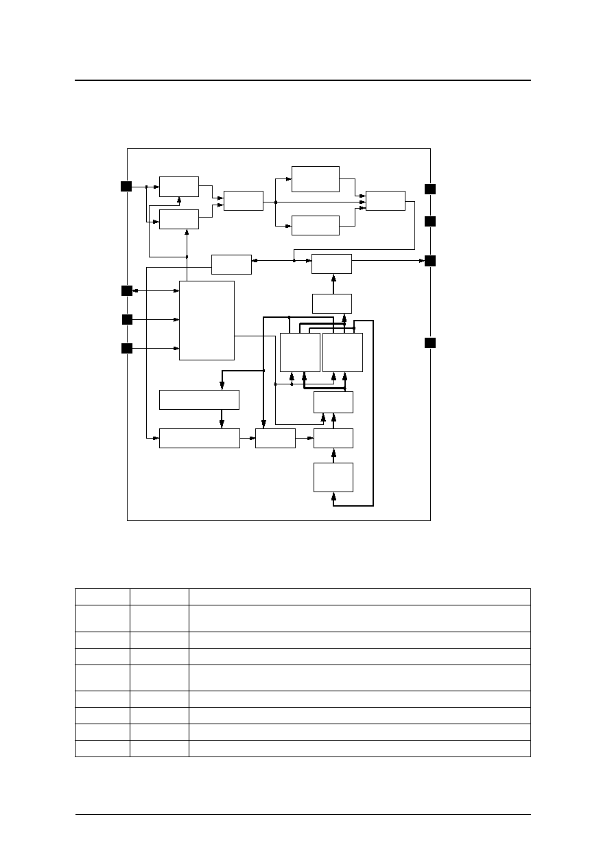
BLOCK DIAGRAM
PIN DESCRIPTION
N u m b e r
N a m e
Function
1
OSC
Built-in RC oscillator option: External resistor and capacitor connection pins
External clock input option: External reference clock input (gate circuit built-in)
2
SIO
Playback control serial interface data input. During parity check, the G flag is output while ST is HIGH.
3
SC
Playback control serial interface clock input
4
ST
Play mode: Playback start/stop control signal input
Write mode: Serial interface data write control signal input
5
TEST
Test input. Pull-down resistor built-in. Leave open or connect to VSS.
6
MTO
Playback melody signal output
7
VDD
Supply
8
VSS
Ground
Gate
Frequency
Multiplier
SW2
Divider
Scale
Counter
Scale
ROM
Tempo Latch
Tempo Counter
Rhythm
Counter
Address
Counter
Start
Address
Latch
Main
ROM
Control
Circuit
OSC
SIO
SC
ST
VSS
VDD
MTO
TEST
Multi-
Plexer
OSC
SW1
Divider
Main
RAM
Master slice
Master slice
(Pull-down resistance
built-in)
SM1126 Series
NIPPON PRECISION CIRCUITS--3
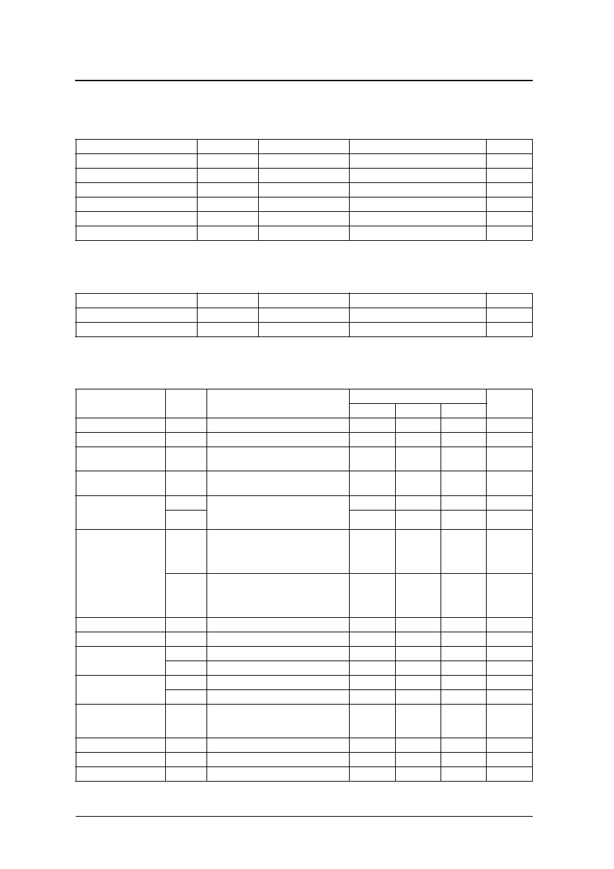
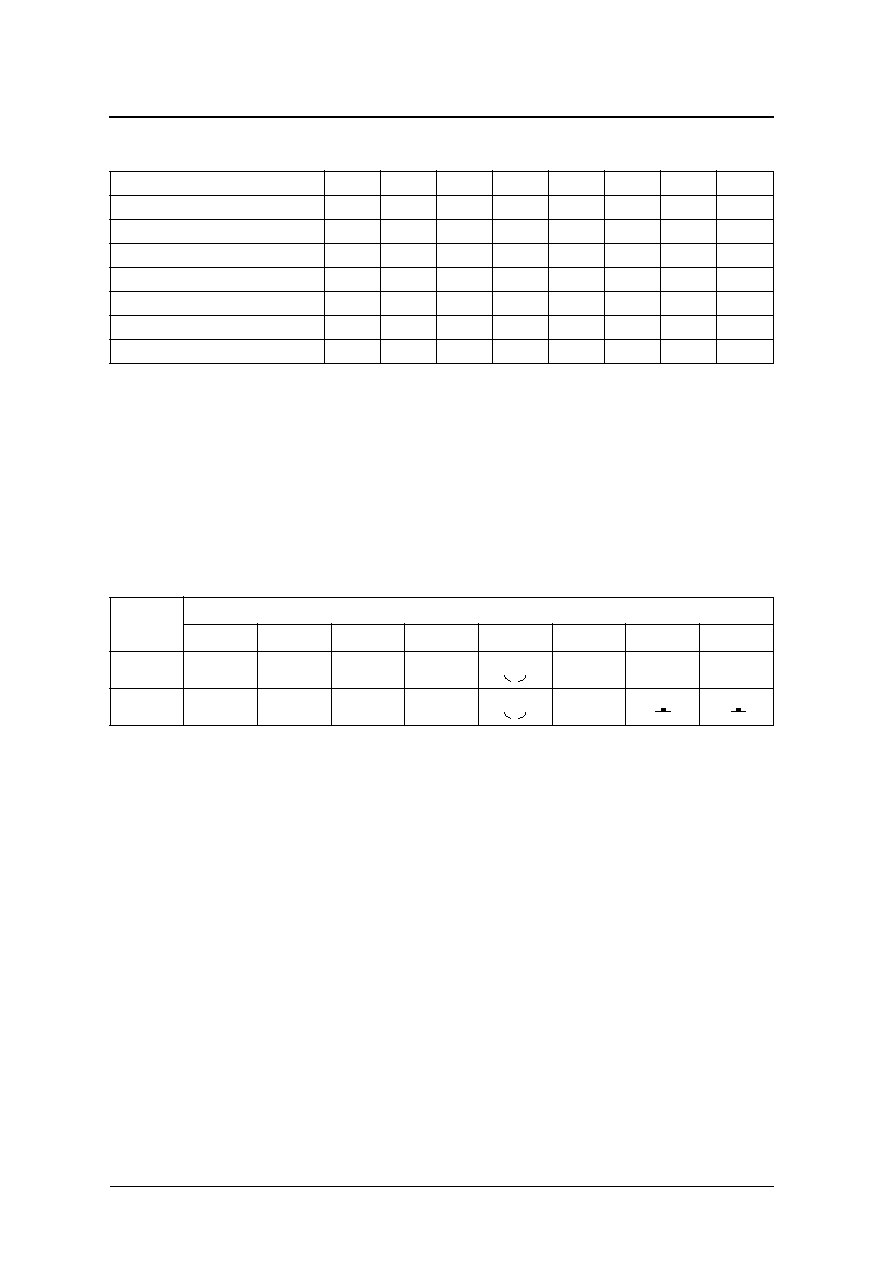
SPECIFICATIONS
Absolute Maximum Ratings
Recommended Operating Conditions
V
SS
= 0 V
DC Characteristics
T
a
=
-
20 to 70
∞
C, V
SS
= 0 V, V
DD
= 2.0 to 3.6 V
P arameter
S y m b o l
Condition
Rating
Unit
Supply voltage range
V
DD
-
V
SS
-
0.3 to 5.0
V
Input voltage range
V
IN
V
SS
-
0.2 to V
DD
+ 0.2
V
Power dissipation
P
D
100
mW
Storage temperature range
T
stg
-
40 to 125
∞
C
Soldering temperature
T
sld
255
∞
C
Soldering time
t
sld
10
s
P arameter
S y m b o l
Condition
Rating
Unit
Supply voltage
V
DD
2.0 to 3.6
V
Operating temperature
T
opr
-
20 to 70
∞
C
P arameter
S y m b o l
Condition
Rating
Unit
m i n
typ
m a x
Supply voltage
V
DD
2.0
3.0
3.6
V
Current consumption (1)
I
DD1
Non-playback mode, T
a
= 25
∞
C
≠
≠
0.5
µA
Current consumption (2)
I
DD2
External clock input option: Playback mode,
MTO pin open
≠
25
200
µA
Current consumption (3)
I
DD3
Built-in RC oscillator option: Playback mode,
MTO pin open
≠
215
600
µA
Input voltage
V
IH
External clock input option: ST, SIO, SC and
OSC pins, Built-in RC oscillator option: ST,
SIO and SC pins
V
DD
-
0.2
≠
V
DD
V
V
IL
V
SS
≠
V
SS
+ 0.2
V
Input current (1)
I
IH1
V
IH
= V
DD
, T
a
= 25
∞
C
External clock input option: ST, SIO, SC and
OSC pins, Built-in RC oscillator option: ST,
SIO and SC pins
≠
≠
0.5
µA
I
IL1
V
IL
= 0 V, T
a
= 25
∞
C
External clock input option: ST, SIO, SC and
OSC pins, Built-in RC oscillator option: ST,
SIO and SC pins
≠
≠
0.5
µA
Input current (2)
I
IH2
TEST pin, V
IH
= V
DD
≠
≠
200
µA
Start voltage
V
OPN
TEST pin
≠
≠
0.1
V
Output voltage (1)
V
OH1
SIO pin, I
OH1
= 1 mA, V
DD
= 2.4 V
V
DD
-
0.4
≠
V
DD
V
V
OL1
SIO pin, I
OL1
= 1 mA, V
DD
= 2.4 V
V
SS
≠
V
SS
+ 0.4
V
Output voltage (2)
V
OH2
MTO pin, I
OH2
= 1 mA
V
DD
-
0.4
≠
V
DD
V
V
OL2
MTO pin, I
OL2
= 1 mA
V
SS
≠
V
SS
+ 0.4
V
Oscillator frequency
f
OSC
Built-in RC oscillator option: NPC test board
measurement, V
DD
= 3.0 V, R
O
= 82 k
,
C
O
= 130 pF
117.965
131.072
144.179
kHz
Frequency stability
f/f
Built-in RC oscillator option
≠
0.2
≠
%/0.1V
Oscillator start voltage
V
DOB
Built-in RC oscillator option
≠
≠
1.6
V
Oscillator stop voltage
V
DOS
Built-in RC oscillator option
≠
≠
1.6
V
SM1126 Series
NIPPON PRECISION CIRCUITS--4
AC Characteristics
T
a
=
-
20 to 70
∞
C, V
SS
= 0 V, V
DD
= 2.0 to 3.6 V
OSC input pulse (external clock input version)
SC input pulse
P arameter
S y m b o l
Condition
Rating
Unit
m i n
typ
m a x
OSC pulse cycle
t
OSC
"OSC input pulse (external clock
input version)" timing
4.0
≠
≠
µs
OSC HIGH-level pulsewidth
t
OWH
2.0
≠
≠
µs
OSC LOW-level pulsewidth
t
OWL
2.0
≠
≠
µs
OSC pulse rise time
t
Or
≠
≠
200
ns
OSC pulse fall time
t
Of
≠
≠
200
ns
SC pulsewidth
t
SC
"SC input pulse" timing
4.0
≠
≠
µs
SC HIGH-level pulsewidth
t
SWH
2.0
≠
≠
µs
SC LOW-level pulsewidth
t
SWL
2.0
≠
≠
µs
SC pulse rise time
t
Sr
≠
≠
200
ns
SC pulse fall time
t
Sf
≠
≠
200
ns
SIO-SC setup time
t
DS
"SC-SIO-ST serial input pulse"
timing
2.0
≠
≠
µs
SIO-SC hold time
t
DH
2.0
≠
≠
µs
ST input write pulsewidth
t
WP
2.0
≠
≠
µs
ST input write pulse rise time
t
Wr
≠
≠
200
ns
ST input write pulse fall time
t
Wf
≠
≠
200
ns
SIO output enable delay
t
OE
"SIO parity check G-flag output
data" timing
≠
≠
600
ns
SIO output disable delay
t
OD
≠
≠
600
ns
V
DD
V
SS
0.5V
DD
t
Of
t
Or
OWH
t
t
OSC
t
0.1V
DD
0.9V
DD
OWL
V
DD
V
SS
OWL
0.5V
DD
t
Sf
t
Sr
SWH
t
SWL
t
SC
t
0.1V
DD
0.9V
DD
SM1126 Series
NIPPON PRECISION CIRCUITS--5
SC-SIO-ST serial input pulse
SIO parity check G-flag output data
ST must be set to LOW when switching ST
ST must be set to LOW when switching ST
SC
SIO
DS
t
DH
t
ST
0.9V
DD
0.1V
DD
Wr
t
WP
t
Wf
t
V
DD
V
SS
0.5V
DD
V
DD
V
SS
0.5V
DD
V
DD
V
SS
0.5V
DD
SC
SIO
ST
V
DD
V
SS
0.5V
DD
V
DD
V
SS
0.5V
DD
V
DD
V
SS
0.5V
DD
INPUT MODE
OUTPUT MODE (G FLAG OUTPUT)
INPUT MODE
OE
t
OD
t
0.9V
DD
0.1V
DD
0.1V
DD
0.9V
DD
SM1126 Series
NIPPON PRECISION CIRCUITS--6
FUNCTIONAL DESCRIPTION
Control Functions
External reference clock
SM1126 Series devices are available in external clock input versions and built-in RC oscillator versions, set
by master-slice option. In the case of the built-in RC oscillator option, an external resistor and capacitor is
required for the oscillator function.
SM1126 Series devices can operate at 6 selectable reference clock frequencies. All melodies playback at the
fixed speed set by the reference clock frequency. External clock input versions operate at one of 6 selectable
clock frequencies, as shown in table 1. Built-in RC oscillator versions operate at only one oscillator frequen-
cies--131.072 kHz.
Power-save function
In external clock input versions, the external reference clock input is used during playback mode only and is
otherwise ignored. If a clock signal is input when not in playback mode (when ST is LOW), the gate circuit
switches to cutoff the external reference clock signal from entering the device, preventing unwanted current
flow.
In built-in RC oscillator versions, the oscillator is stopped when not in playback mode (when ST is LOW),
preventing unwanted current flow.
Table 1. Reference clock frequencies (external clock)
F r e q u e n c y
s y s t e m
Selectable frequencies
32.768 kHz
32.768 kHz
65.536 kHz
131.072 kHz
38.4 kHz
38.4 kHz
76.8 kHz
153.6 kHz
Figure 1. External clock input version: OSC input during playback mode only
Figure 2. External clock input version: Continuous OSC input
Figure 3. Built-in RC oscillator version
ST
OSC
ST
OSC
ST
OSC
CR
Oscillation

SM1126 Series
NIPPON PRECISION CIRCUITS--7
Serial inputs
Serial data is input on SIO in sync with the SC clock in 8-bit units when ST is LOW. Data is not accepted
when ST is HIGH. When ST goes HIGH, the 8-bit data is latched. Note that if the input data exceeds 8 bits in
length, the most recent 8 bits are used and any preceding bits are ignored. Data is in MSB first format.
Input data is interpreted as a command or as a data word (in write mode), depending on the current operating
mode of the device. There are 3 types of commands:
s
Playback start command
s
SRAM write command
s
End-of-write command
The SRAM write command is used to invoke write mode operation, and end-of-write command is used to
return to play mode operation. In write mode, however, data is interpreted as data words to be written to
SRAM.
Note that pin SIO is an output pin only when the parity check command is executed. At all other times, SIO
is an input pin.
Playback control
The ST pin controls the start of playback. While ST is HIGH, the melody is played repeatedly, and when ST
goes LOW, playback stops. Melodies are selected by input serial data on pins SIO and SC, as shown in table 2.
The melody select command comprises a fixed code (1000) followed by 4 melody select data bits (B3 to B0).
The 8 bits of data are retained even after playback. If serial data is input during playback, the data is ignored
and playback continues.
Pin SC should be LOW when either a LOW-to-HIGH or HIGH-to-LOW transition occurs on pin ST.
Figure 4. Serial input timing
Pin SC should be LOW when either a LOW-to-HIGH or HIGH-to-LOW transition occurs on pin ST.
Figure 5. Serial data input timing
SIO
SC
ST
Invalid
Data
Invalid
Data
?
?
B3 B2 B1 B0
B7 B6 B5 B4
?
?
?
?
?
?
?
?
?
?
Valid
Data
SIO
SC
ST
MTO
Invalid
Data
Invalid
Data
?
?
B3 B2 B1 B0
H L L L
?
?
?
?
?
?
?
?
?
?
Valid
Data
SM1126 Series
NIPPON PRECISION CIRCUITS--8
Table 2. Serial data melody select
B 3
B 2
B 1
B 0
S T
M e l o d y
B 3
B 2
B 1
B 0
S T
M e l o d y
L
L
L
L
L
H
1st melody
H
L
L
L
L
H
9th melody
L
L
L
H
L
H
2nd melody
H
L
L
H
L
H
10th melody
L
L
H
L
L
H
3rd melody
H
L
H
L
L
H
11th melody
L
L
H
H
L
H
4th melody
H
L
H
H
L
H
12th melody
L
H
L
L
L
H
5th melody
H
H
L
L
L
H
13th melody
L
H
L
H
L
H
6th melody
H
H
L
H
L
H
14th melody
L
H
H
L
L
H
7th melody
H
H
H
L
L
H
15th melody
L
H
H
H
L
H
8th melody
H
H
H
H
L
H
SRAM melody
Melody plays repeatedly when ST is HIGH, and stops immediately when ST goes LOW.
Figure 6. Melody repetition timing
SIO
SC
ST
MTO
#n1 Data
#n2 Data
#n1 Play
#n1 Play
#n1 Play
#n2 Play

SM1126 Series
NIPPON PRECISION CIRCUITS--9
Playback timing diagrams
Playback start
Playback starts after an interval t
ST
after ST goes HIGH.
When the reference clock frequency is 32.768 kHz, t
ST
= (256 ± 1 oscillator cycles) + 1/128 seconds.
When the reference clock frequency is 38.4 kHz, t
ST
= (300 ± 1 oscillator cycles) + 1/128 seconds.
Playback stop
Playback stops immediately when ST goes LOW. In external clock input versions, the IC internal clock also
stops when ST goes LOW, regardless of whether or not there is a clock input signal on pin OSC. In built-in RC
oscillator versions, the oscillator also stops when ST goes LOW.
Figure 7. Playback start timing
Figure 8. Stop timing
SIO
SC
ST
MTO
MSB
LSB
Play Start Command
OSC
*Internal
Clock
,,,,,
,,,,,
,,,,,
256(300) 1 Clock
1/128 sec
,,,,,,,,,,,,,,,,,
,,,,,,,,,,,,,,,,,
,,,,,,,,,,,,,,,,,
ST
MTO
OSC
*Internal
Clock

SM1126 Series
NIPPON PRECISION CIRCUITS--10
Write Mode Control
Write sequence
The SM1126 Series devices can accept data words written to the built-in SRAM to play any melody. The
SRAM write sequence is described below.
1. Write the SRAM write command (11011111) to invoke write mode.
2. Write the tempo word (parity check ON/OFF selectable).
3. Write all necessary melody data words (parity check ON/OFF selectable).
4. Write the melody end word (parity check ON/OFF selectable).
5. Optionally, write extra data words (these are ignored).
6. Write the end-of-write command (10111111) to return to play mode.
7. If parity check was ON, write the parity check command (01111111) to perform an error check.
The built-in SRAM can store 64 words, so all melody and end words must fit within this limit. Note that the
tempo word is not stored in SRAM, but in a separate register. Playback of melodies stored in SRAM begins
from the SRAM leading address and continues until the end word is detected, at which point playback contin-
ues again from the SRAM leading address. All data in SRAM after the end word is ignored.
Figure 9. Write control sequence
Input parity check command (01111111)
Input end-of-write command (10111111)
Write optional invalid data
Write end word
Write melody word (s)
Write tempo word
Input write command (11011111)
Input end-of-write command (10111111)
Write optional invalid data
Write end word
Write melody word (s)
Write tempo word
Input write command (11011111)
Play mode
Play mode
Example 1. Parity check selected
Example 2. Parity check not selected
Write mode

SM1126 Series
NIPPON PRECISION CIRCUITS--11
Write command
The SRAM write command (11011111), shown below, is used to invoke write mode.
Tempo word
The tempo word controls the melody playback speed. The tempo word comprises a fixed code (000) fol-
lowed by the tempo code (T4 to T0), as shown below. The tempo word is always the first word written after
invoking write mode, and all subsequent words are melody data words.
Figure 10. Write command timing
Figure 11. Tempo word timing
SIO
SC
ST
PLAY mode changed to WRITE mode
Address set to tempo-word register
1
0
1
1
1
1
1
1
SIO
SC
ST
0
T4
WRITE command
Changed to WRITE mode
write Tempo-word
Tempo Register Address
No Address
RAM Address
ADDRESS
0
0
T3
T2
T1
T0
SM1126 Series
NIPPON PRECISION CIRCUITS--12
Melody words
Melody words contain all the information needed for playback of a single note, including the note duration
and type (name or rest). Each melody word comprises a 3-bit length code (R2 to R0) followed by a 5-bit type
code (S4 to S0).
End word
The end word (01011111) indicates the end of the melody. When the end word is detected during melody
playback, operation returns to the SRAM leading address. All data in SRAM after the end word is ignored.
End-of-write command
The end-of-write command (10111111) is used to return to play mode from write mode. This command
should be executed when power is first applied to set play mode.
Figure 12. Melody word timing
Figure 13. End word timing
Figure 14. End-of-write command timing
SIO
SC
ST
ADDRESS
(n)th data
n
n-1
write (n-1)th Data
write (n)th data
n+1
(n-1)th data
SIO
SC
ST
0
1
ADDRESS
0
1
1
1
1
1
next word
m+1
m
write END-WORD
write next word
m+2
SIO
SC
ST
WRITE mode changed to PLAY mode
0
1
1
1
1
1
1
1
SM1126 Series
NIPPON PRECISION CIRCUITS--13
Parity check command
Data words (tempo word, melody words, end word) can have an optional parity bit added, forming 9-bit data
words, for a parity check function. The parity check command is executed in play mode, immediately after the
end-of-write command is executed.
The parity bit is added at the beginning of the data word. Note that the last 8 bits are always the valid data
bits. The parity check function performs an odd parity check (an odd number of 1s within the 9-bit data). If the
parity check command is not executed, play mode operation continues using the valid 8 bits of data in each
data word.
The parity check sequence is described below.
1. The internal G flag (Good flag) is set to 1 when the write command is executed.
2. When writing data words, the G flag remains set to 1 for odd parity, but is set to 0 if even parity is detected.
3. The G flag remains set to 1 only if all data words have odd parity.
4. Write the end-of-write command to return to play mode.
5. Write the parity check command.
6. When ST is HIGH, the SIO pin functions as the G flag output.
7. When ST goes LOW, the G flag output is released.
Figure 15. Parity check timing
SIO
SC
ST
MODE
SIO Condition
G Flag
WRITE mode
Input
PLAY mode
0
1
1
1
1
1
1
1
1
1
0
1
1
1
1
1
END-WRITE mode command
Parity Check Command
Input
Output
When G Flag = 1
When G Flag = 0
SM1126 Series
NIPPON PRECISION CIRCUITS--14
Command summary
Musical Specifications
Maximum program steps
A maximum of 256 steps can be programmed into mask-programmable ROM, and a maximum of 64 steps
(including one end word) can be stored in built-in SRAM. Each step represents either a note (sound pitch and
length) a rest, or a tie.
Note length (including rests)
Eight rhythm values for notes and rests can be programmed. Also, 2 or more notes can be musically tied.
Pitch and scale
SM1126 Series devices support 27 pitches from F4 to G6. The pitch varies with the clock frequency, as
shown in the frequency listing in table 4. The reference clock selected at master-slice does not affect the pitch
range.
Also, two pitches higher than G6 can be set as alarm pitches in mask ROM. Note that an alarm pitch option
cannot be specified in SRAM.
The frequency error calculation for a given pitch is shown below.
Error calculation: (A4 pitch with 32.768 kHz clock)
C o m m a n d
M S B
Bit 6
Bit 5
Bit 4
Bit 3
Bit 2
Bit 1
L S B
Melody start command
1
0
0
0
B3
B2
B1
B0
Write command
1
1
0
1
1
1
1
1
Tempo word
0
0
0
T4
T3
T2
T1
T0
Melody word
R2
R1
R0
S4
S3
S2
S1
S0
End word
0
1
0
1
1
1
1
1
End-of-write command
1
0
1
1
1
1
1
1
Parity check command
0
1
1
1
1
1
1
1
Table 3. Rhythm values
Ty p e
C o d e
0
1
2
3
4
5
6
7
N o t e
R e s t
1200
log
2
Output frequency
Reference frequency
-------------------------------------------------
◊
1200
log
10
Output frequency
Reference frequency
-------------------------------------------------
log
10
2
---------------------------------------------------------------
◊
=
3986.3
log
10
Output frequency
Reference frequency
-------------------------------------------------
◊
3986.3
log
10
439.839
440.000
-------------------
◊
0.63 cent
≠
SM1126 Series
NIPPON PRECISION CIRCUITS--15
(Note) A4 is the following note.
Pitches AL1 and AL2 are optional alarm pitches which can take any value higher than G6, set in mask ROM.
This option is not supported in SRAM.
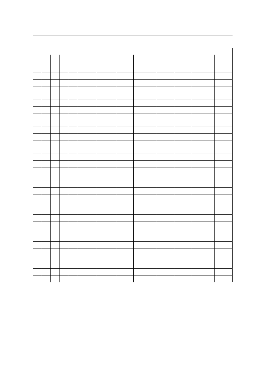
Table 4. Frequency range
N o t e c o d e
S y s t e m clock
32.768 kHz system
38.4 kHz system
S 4
S 3
S 2
S 1
S 0
Pitch
R e ference
frequency
F r e q u e n c y
divider
F r e q u e n c y
(Hz)
Relative
error (cent)
F r e q u e n c y
divider
F r e q u e n c y
(Hz)
Relative
error (cent)
0
0
0
0
0
Rest
≠
≠
≠
≠
≠
≠
≠
0
0
0
0
1
F4
349.228
188
348.596
-
3.14
220
349.091
-
0.68
0
0
0
1
0
F#4
369.994
177
370.260
1.24
208
369.231
-
3.58
0
0
0
1
1
G4
391.995
167
392.431
1.92
196
391.837
-
0.70
0
0
1
0
0
G#4
415.305
158
414.785
-
2.17
185
415.135
-
0.71
0
0
1
0
1
A4
440.000
149
439.839
-
0.63
175
438.857
-
4.50
0
0
1
1
0
A#4
466.164
141
464.794
-
5.09
165
465.455
-
2.64
0
0
1
1
1
B4
493.883
133
492.752
-
3.97
156
492.308
-
5.53
0
1
0
0
0
C5
523.251
125
524.288
3.43
147
522.449
-
2.66
0
1
0
0
1
C#5
554.365
118
555.390
3.20
139
552.518
-
5.78
0
1
0
1
0
D5
587.330
112
585.143
-
6.46
131
586.260
-
3.16
0
1
0
1
1
D#5
622.254
105
624.152
5.27
123
624.390
5.93
0
1
1
0
0
E5
659.255
99
661.980
7.14
116
662.069
7.37
0
1
1
0
1
F5
698.456
94
697.191
-
3.14
110
698.182
-
0.68
0
1
1
1
0
F#5
739.989
89
736.360
-
8.51
104
738.462
-
3.58
0
1
1
1
1
G5
783.991
84
780.190
-
8.41
98
783.673
-
0.70
1
0
0
0
0
G#5
830.609
79
829.570
-
2.17
92
834.783
8.68
1
0
0
0
1
A5
880.000
74
885.622
11.02
87
882.759
5.42
1
0
0
1
0
A#5
932.328
70
936.229
7.23
82
936.585
7.89
1
0
0
1
1
B5
987.767
66
992.970
9.10
78
984.615
-
5.53
1
0
1
0
0
C6
1046.502
63
1040.254
-
10.37
73
1052.055
9.16
1
0
1
0
1
C#6
1108.731
59
1110.780
3.20
69
1113.043
6.72
1
0
1
1
0
D6
1174.659
56
1170.286
-
6.46
65
1181.538
10.11
1
0
1
1
1
D#6
1244.508
53
1236.528
-
11.14
62
1238.710
-
8.08
1
1
0
0
0
E6
1318.510
50
1310.720
-
10.26
58
1324.138
7.37
1
1
0
0
1
F6
1396.913
47
1394.383
-
3.14
55
1396.364
-
0.68
1
1
0
1
0
F#6
1479.978
44
1489.455
11.05
52
1476.923
-
3.58
1
1
0
1
1
G6
1567.982
42
1560.381
-
8.41
49
1567.347
-
0.70
1
1
1
0
0
AL1
≠
≠
≠
≠
≠
≠
≠
1
1
1
0
1
AL2
≠
≠
≠
≠
≠
≠
≠
1
1
1
1
0
Tie
≠
≠
≠
≠
≠
≠
≠
1
1
1
1
1
End word
≠
≠
≠
≠
≠
≠
≠
A4 (440Hz)

SM1126 Series
NIPPON PRECISION CIRCUITS--16
Tempo
There are 29 tempos that can be selected for each melody. The tempo does not vary with the clock frequency.
Quarter note (
) length = {1536 (32.768 kHz system) or 1800 (38.4 kHz system)}
◊
tempo counter frequency
divider ˜ clock frequency
(Ex. 1) Tempo code = 1F (divider = 32), clock frequency = 32.768 kHz (32.768 kHz system)
1536
◊
32 ˜ 32768 = 1.5 (seconds)
(Ex. 2) Tempo code = 18 (divider = 25), CLK frequency = 153.6 kHz (38.4 kHz system)
1800
◊
25 ˜ 38400 = 1.17 (seconds)
Table 5. Tempo range
C o d e
F r e q u e n c y divider
Te m p o
=
03
4
Prestissimo
320.0
04
5
256.0
05
6
213.3
06
7
Presto
182.9
07
8
Allegro
160.0
08
9
142.2
09
10
128.0
0A
11
Moderato
116.4
0B
12
106.7
0C
13
Andante
98.5
0D
14
91.4
0E
15
85.3
0F
16
80.0
10
17
Adagio
75.3
11
18
71.1
12
19
67.4
13
20
Larghetto
64.0
14
21
61.0
15
22
Largo
58.2
16
23
55.7
17
24
53.3
18
25
51.2
19
26
49.2
1A
27
47.4
1B
28
45.7
1C
29
44.1
1D
30
42.7
1E
31
41.3
1F
32
40.0
SM1126 Series
NIPPON PRECISION CIRCUITS--17
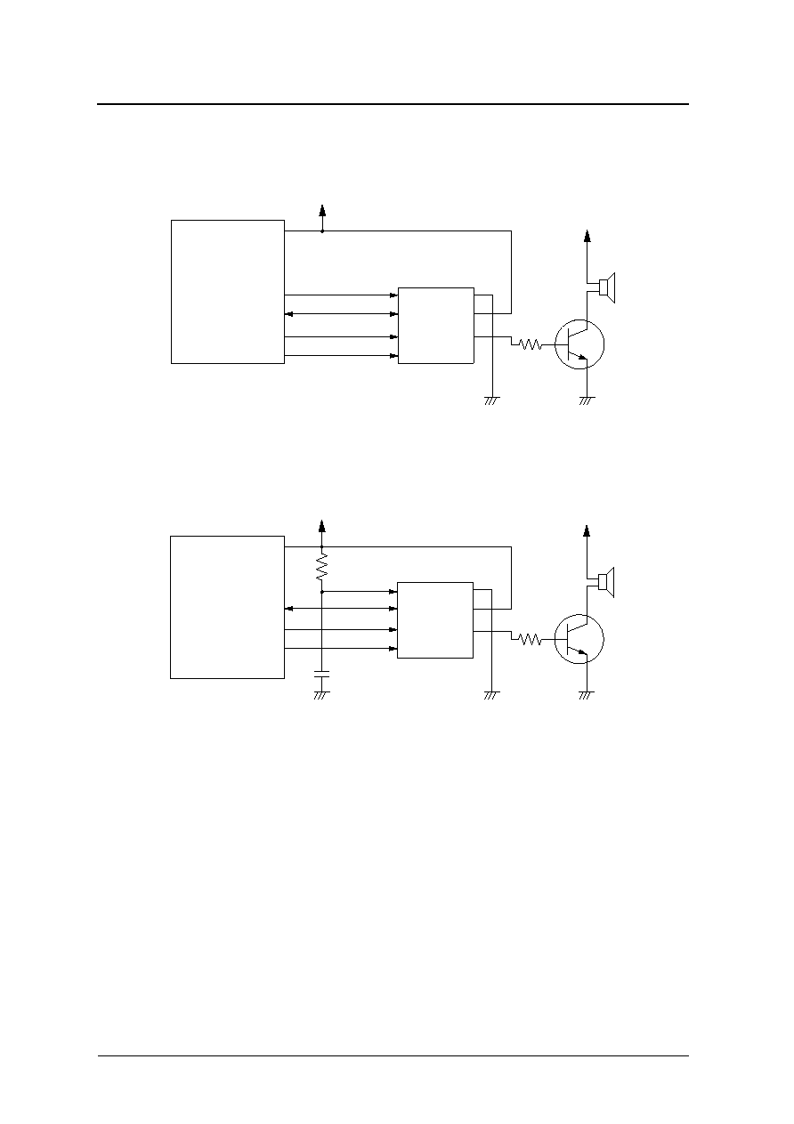
TYPICAL APPLICATION
External Clock Input Versions
Built-in RC Oscillator Versions
OSC
SIO
SC
ST
V
DD
VSS
MTO
TEST
2.0V to 3.6V
B
+
CONTROLLER
OSC
SIO
SC
ST
V
DD
VSS
MTO
TEST
2.0 to 3.6V
B
+
R
O
CONTROLLER
C
O
SM1126 Series
NIPPON PRECISION CIRCUITS--18
NIPPON PRECISION CIRCUITS INC. reserves the right to make changes to the products described in this data sheet in order to
improve the design or performance and to supply the best possible products. Nippon Precision Circuits Inc. assumes no responsibility for
the use of any circuits shown in this data sheet, conveys no license under any patent or other rights, and makes no claim that the circuits
are free from patent infringement. Applications for any devices shown in this data sheet are for illustration only and Nippon Precision
Circuits Inc. makes no claim or warranty that such applications will be suitable for the use specified without further testing or modification.
The products described in this data sheet are not intended to use for the apparatus which influence human lives due to the failure or
malfunction of the products. Customers are requested to comply with applicable laws and regulations in effect now and hereinafter,
including compliance with export controls on the distribution or dissemination of the products. Customers shall not export, directly or
indirectly, any products without first obtaining required licenses and approvals from appropriate government agencies.
NIPPON PRECISION CIRCUITS INC.
4-3, Fukuzumi 2-chome
Koto-ku, Tokyo 135-8430, Japan
Telephone: 03-3642-6661
Facsimile: 03-3642-6698
NC9722BE
1998.12
NIPPON PRECISION CIRCUITS INC.
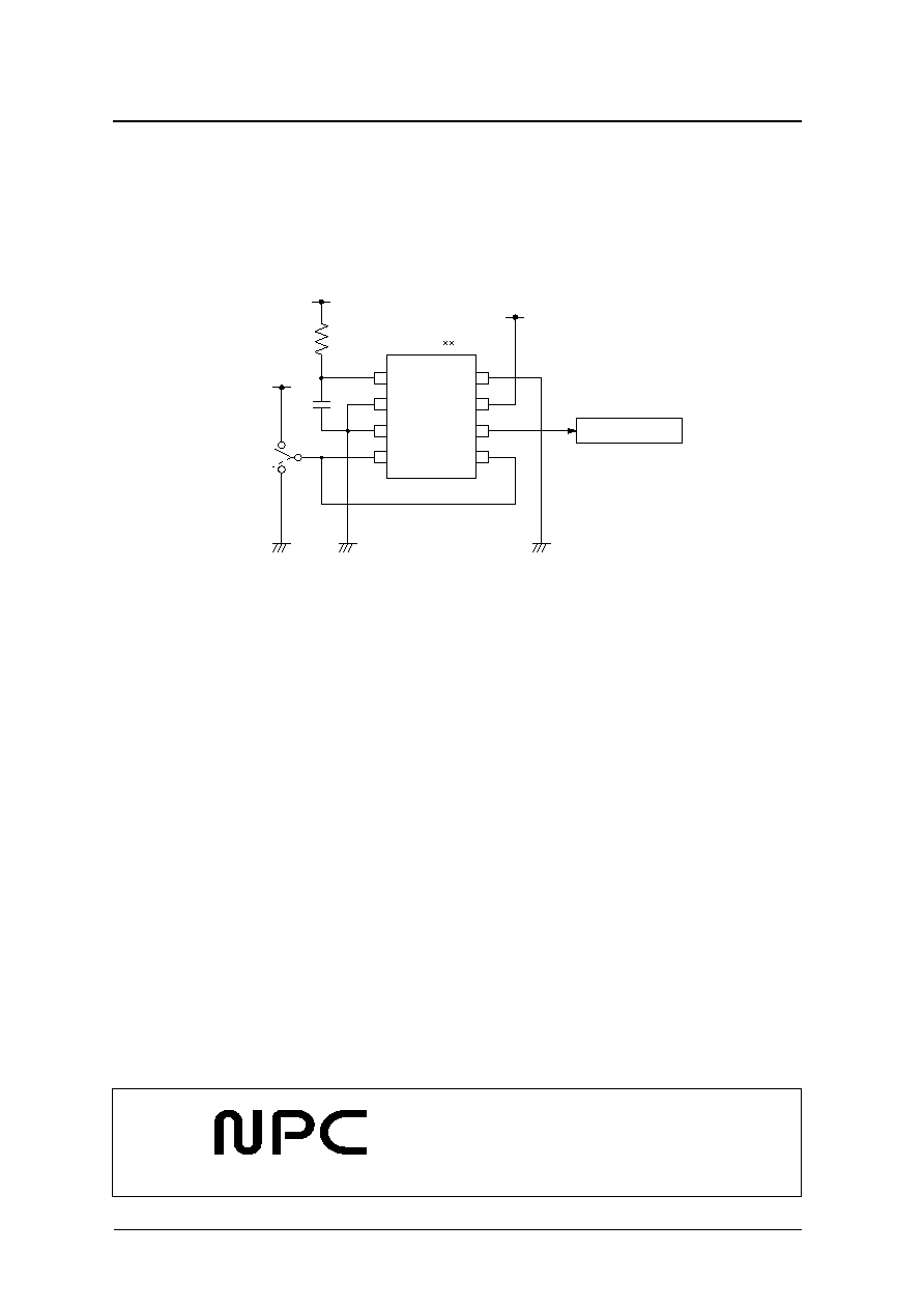
OSCILLATOR FREQUENCY MEASUREMENT
The measurement circuit below shows a SM1126
◊◊
V with built-in RC oscillator circuit and external RC
oscillator components capacitor C
O
and resistor R
O
.
When ST is switched to V
DD
, the oscillator starts and outputs a pulse on MTO with a frequency double that
of the RC oscillator. The output pulse is counted using a frequency counter.
Note that the board mounting and wiring will marginally affect the output frequency, even for equivalent values for R
O
and C
O
.
OSC
SIO
SC
ST
V
DD
V
SS
MTO
TEST
R
O
C
O
Switch
Frequency Counter
SM1126 V