SM5009 series
NIPPON PRECISION CIRCUITS--1
NIPPON PRECISION CIRCUITS INC.
Crystal Oscillator Module ICs
OVERVIEW
The SM5009 series are crystal oscillator module ICs, that incorporate circuits to limit oscillator-stage current,
controlling total current consumption. High-frequency capacitors are built-in, eliminating the need for external
components to make a stable fundamental-harmonic oscillator.
FEATURES
I
Capacitors C
G
, C
D
built-in
I
Standby function
I
6
�
A typ (V
DD
=
5 V) low standby current
(SM5009AL
�
S)
I
Power-save pull-up resistor built-in
(SM5009AL
�
S)
I
Inverter amplifier feedback resistor built-in
I
16 mA (V
DD
=
4.5 V) drive capability
(SM5009AK
�
S, AL
�
S, AN
�
S, CN
�
S)
I
4 mA (V
DD
=
4.5 V) drive capability
(SM5009AH
�
S)
I
Output three-state function
I
2.25 to 5.5 V supply voltage (CF5009AL
�
)
I
2.7 to 5.5 V supply voltage
(SM5009AH
�
S, AL
�
S, AN
�
S, CN
�
S)
I
Oscillator frequency output (f
O
, f
O
/2, f
O
/4, f
O
/8,
f
O
/16, f
O
/32 determined by internal connection)
I
8-pin SOP (SM5009
���
S)
I
Chip form (CF5009
���
)
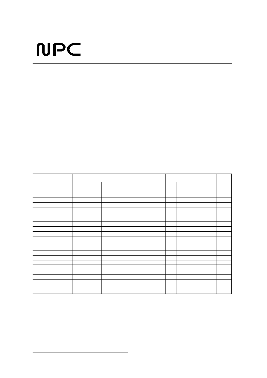
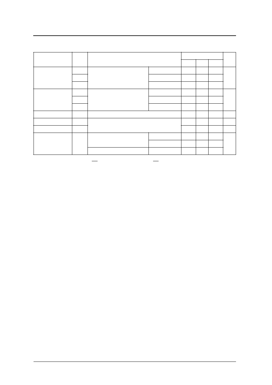
SERIES CONFIGURATION
Note: R e c o m m e n d e d o p e rating frequency is not the guaranteed value but is measured using NPC's standard crystal.
ORDERING INFORMATION
V ersion
1 , 2
1. Chip form d evices have designation CF5009
���
.
2. S M 5 0 0 9 A H
�
S: V
D D
= 4.5 to 5.5V
S M 5 0 0 9 A K
�
S: Ta = �20 to +85
�
C
S u p p ly
voltag e
[V]
Output
frequency
3V operating
5V operating
Built-in
capacitance
Input
level
Output
duty
level
S t a n d by
function
Output
load
(max)
[pF]
R e c o m m e n d e d
operating
frequency
r a n g e
3
[MHz]
3. S M 5 0 0 9 A H
�
S , AN
�
S , AL
�
S: Ta = �20 to +80
�
C
S M 5 0 0 9 C N
�
S: Ta = �10 to +70
�
C
Output
load
(max)
[pF]
R e c o m m e n d e d
operating
frequency
r a n g e
4
[MHz]
4. S M 5 0 0 9 A N
�
S , AL
�
S: Ta = �20 to +80
�
C
C
G
[pF]
C
D
[pF]
S M 5 0 0 9 A H 1 S
2.7 to 5.5
f
O
1 5
1 6
1 5
3 0
6
1 0
T T L
C M O S
N o
S M 5 0 0 9 A H 2 S
2.7 to 5.5
f
O
/2
1 5
1 6
1 5
3 0
6
1 0
T T L
C M O S
N o
S M 5 0 0 9 A H 3 S
2.7 to 5.5
f
O
/4
1 5
1 6
1 5
3 0
6
1 0
T T L
C M O S
N o
S M 5 0 0 9 A H 4 S
2.7 to 5.5
f
O
/8
1 5
1 6
1 5
3 0
6
1 0
T T L
C M O S
N o
S M 5 0 0 9 A K 1 S
4.5 to 5.5
f
O
�
�
1 5
4 0
6
1 0
T T L
T T L
N o
S M 5 0 0 9 A K 2 S
4.5 to 5.5
f
O
/2
�
�
1 5
4 0
6
1 0
T T L
T T L
N o
S M 5 0 0 9 A N 1 S
2.7 to 5.5
f
O
3 0
4 0
5 0
4 0
6
1 0
T T L
C M O S
N o
S M 5 0 0 9 A N 2 S
2.7 to 5.5
f
O
/2
3 0
4 0
5 0
4 0
6
1 0
T T L
C M O S
N o
S M 5 0 0 9 A N 3 S
2.7 to 5.5
f
O
/4
3 0
4 0
5 0
4 0
6
1 0
T T L
C M O S
N o
S M 5 0 0 9 A N 4 S
2.7 to 5.5
f
O
/8
3 0
4 0
5 0
4 0
6
1 0
T T L
C M O S
N o
S M 5 0 0 9 A N 5 S
2.7 to 5.5
f
O
/16
3 0
4 0
5 0
4 0
6
1 0
T T L
C M O S
N o
S M 5 0 0 9 A N 6 S
2.7 to 5.5
f
O
/32
3 0
4 0
5 0
4 0
6
1 0
T T L
C M O S
N o
S M 5 0 0 9 C N 1 S
2.7 to 5.5
f
O
1 5
3 0
5 0
3 0
6
1 0
T T L
C M O S
N o
S M 5 0 0 9 C N 2 S
2.7 to 5.5
f
O
/2
1 5
3 0
5 0
3 0
6
1 0
T T L
C M O S
N o
S M 5 0 0 9 A L 1 S
2.7 to 5.5
f
O
3 0
4 0
5 0
4 0
6
1 0
C M O S
C M O S
Yes
S M 5 0 0 9 A L 2 S
2.7 to 5.5
f
O
/2
3 0
4 0
5 0
4 0
6
1 0
C M O S
C M O S
Yes
S M 5 0 0 9 A L 3 S
2.7 to 5.5
f
O
/4
3 0
4 0
5 0
4 0
6
1 0
C M O S
C M O S
Yes
S M 5 0 0 9 A L 4 S
2.7 to 5.5
f
O
/8
3 0
4 0
5 0
4 0
6
1 0
C M O S
C M O S
Yes
S M 5 0 0 9 A L 5 S
2.7 to 5.5
f
O
/16
3 0
4 0
5 0
4 0
6
1 0
C M O S
C M O S
Yes
S M 5 0 0 9 A L 6 S
2.7 to 5.5
f
O
/32
3 0
4 0
5 0
4 0
6
1 0
C M O S
C M O S
Yes
D e vice
P a ck ag e
S M 5 0 0 9
���
S
8-pin SOP
C F 5 0 0 9
���
� 1
Chip form
SM5009 series
NIPPON PRECISION CIRCUITS--2
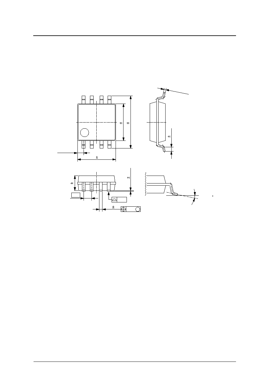
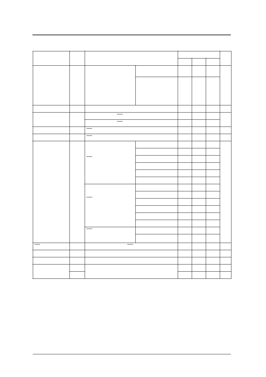
PACKAGE DIMENSIONS
(Unit:mm)
�
8-pin SOP
4.4 0.2
1.5 0.1
0.05 0.05
0.4 0.2
5.2 0.3
0.4 0.1
0.15
+ 0.1
- 0.05
0 to 10
6.2 0.3
0.695typ
1.27
0.12
M
0.10
SM5009 series
NIPPON PRECISION CIRCUITS--3
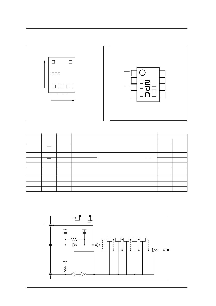
PAD LAYOUT
(Unit:
�
m)
PINOUT
(Top view)
PIN DESCRIPTION and PAD DIMENSIONS
BLOCK DIAGRAM
Chip size: 0.92
�
1.22 mm
Chip thickness: 300 � 30 �m
Chip base: V
D D
level
Q
VDD
XT
VSS
(0,0)
(920,1220)
X
Y
HA5009
INH
XT
1
XT
VSS
Q
VDD
4
2
3
NC
NC
8
7
6
5
009
XT
INH
N u m b e r
N a m e
I/O
Description
P ad dimensions [�m]
X
Y
1
I N H
I
Output state control input. High impedance when LOW . In the case of the
S M 5 0 0 9 A L
�
S , the oscillator stops and Pow er-saving pull-up resistor built in.
1 9 5
2 1 2
2
X T
I
Amplifier input.
Cr ystal oscillator connection pins.
Cr ystal oscillator connected between XT and X T
3 8 5
2 1 2
3
X T
O
Amplifier output.
5 7 5
2 1 2
4
V S S
�
G r o u n d
7 6 6
2 1 2
5
Q
O
Output. Output frequency (f
O
, f
O
/2, f
O
/4, f
O
/8, f
O
/16, f
O
/32) determined by
internal connection
7 6 5
1 0 6 2
6
N C
�
No connection
�
�
7
N C
�
No connection
�
�
8
V D D
�
Supply voltage
1 6 2
1 0 6 2
XT
VSS
VDD
Q
C
G
C
D
R
f
XT
INH
1/2
1/2
1/2
1/2
1/2
SM5009 series
NIPPON PRECISION CIRCUITS--4
SPECIFICATIONS
Absolute Maximum Ratings
V
SS
= 0 V
Recommended Operating Conditions
V
SS
= 0 V
P arameter
S y m b o l
Condition
Rating
Unit
Supply voltage ra n g e
V
D D
-
0.5 to 7.0
V
Input voltage ra n g e
V
IN
-
0.5 to V
D D
+ 0.5
V
Output voltage ra n g e
V
O U T
-
0.5 to V
D D
+ 0.5
V
O p e rating temperature ra n g e
T
opr
-
40 to 85
�
C
Storage temperature ra n g e
T
stg
Chip form
-
65 to 150
�
C
8-pin SOP
-
55 to 125
Output current
I
O U T
2 5
m A
P ow er dissipation
P
D
8-pin SOP
5 0 0
m W
P arameter
S y m b o l
Series
Condition
Rating
Unit
m i n
typ
m a x
Supply voltage
V
D D
AH ser ies
f
3 0 M H z
4.5
�
5.5
V
f
1 6 M H z
2.7
�
3.3
AK ser ies
f
4 0 M H z
4.5
�
5.5
V
AN ser ies
f
4 0 M H z
2.7
�
5.5
V
CN ser ies
f
3 0 M H z
2.7
�
5.5
V
AL series
Chip form
f
4 0 M H z
2.7
�
5.5
V
f
3 0 M H z
2.3
�
2.7
f
2 0 M H z
2.25
�
2.75
8-pin SOP
f
4 0 M H z
2.7
�
5.5
f
14.4MHz
2.4
�
2.7
Input voltage
V
IN
All series
V
S S
�
V
D D
V
O p e rating temperature
T
O P R
AH ser ies
f
30MHz, 4.5V
V
D D
5.5V
- 40
�
+ 85
�C
f
16MHz, 2.7V V
D D
3.6V
- 20
�
+ 80
AK ser ies
f
30MHz
- 40
�
+ 85
�C
3 0 M H z
< f 40MHz
- 20
�
+ 80
AN ser ies
Chip form
f
40MHz, 2.7V V
D D
< 4.5V
- 20
�
+ 80
�C
f
40MHz, 4.5V V
D D
5.5V
- 40
�
+ 85
8-pin SOP
f
40MHz, 2.7V V
D D
< 4.5V
- 20
�
+ 80
f
40MHz, 4.5V V
D D
5.5V
- 20
�
+ 80
f
30MHz, 4.5V V
D D
5.5V
- 40
�
+ 85
CN ser ies
f
30MHz, 2.7V V
D D
< 4.5V
- 10
�
+ 70
�C
f
30MHz, 4.5V V
D D
5.5V
- 40
�
+ 85
AL series
Chip form
f
40MHz, 2.7V V
D D
5.5V
- 40
�
+ 85
�C
f
30MHz, 2.3V V
D D
2.7V
- 20
�
+ 80
f
20MHz, 2.25V V
D D
2.75V
- 20
�
+ 80
8-pin SOP
f
40MHz, 2.7V V
D D
5.5V
- 20
�
+ 80
f
30MHz, 2.7V V
D D
5.5V
- 40
�
+ 85
f
14.4MHz, 2.4V V
D D
2.7V
- 20
�
+ 80
SM5009 series
NIPPON PRECISION CIRCUITS--5
Electrical Characteristics
5009AH series
3 V operation: V
DD
= 2.7 to 3.3 V, V
SS
= 0 V, Ta =
-20 to 80 �C unless otherwise noted.
5 V operation: V
DD
= 4.5 to 5.5 V, V
SS
= 0 V, Ta =
-40 to 85 �C unless otherwise noted.
P arameter
S y m b o l
Condition
Rating
Unit
m i n
typ
m a x
HIGH-level output voltage
V
O H
Q: Measurement cct 1, I
O H
= 2 m A
2.2
�
�
V
L O W -level output voltage
V
O L
Q: Measurement cct 1, I
O L
= 2 m A
�
�
0.4
V
Output leakage current
I
Z
Q: Measurement cct 2, I N H = L O W , V
O H
= V
D D
�
�
1 0
� A
Q: Measurement cct 2, I N H = L O W , V
O L
= V
S S
�
�
1 0
HIGH-level input voltage
V
IH
I N H
2.0
�
�
V
L O W -level input voltage
V
IL
I N H
�
�
0.3
V
Current consumption
I
D D
I N H = open, Measurement cct 3,
load cct 2, C
L
= 15 p F,
16 MHz cr ystal oscillator
S M 5 0 0 9 A H 1 S
C F 5 0 0 9 A H 1
�
4.5
1 0
m A
S M 5 0 0 9 A H 2 S
C F 5 0 0 9 A H 2
�
3
7
S M 5 0 0 9 A H 3 S
C F 5 0 0 9 A H 3
S M 5 0 0 9 A H 4 S
C F 5 0 0 9 A H 4
�
1.5
3
I N H pull-up resistance
R
U P
Measurement cct 4, V
D D
= 3 V, I N H = V
S S
4 0
�
2 0 0
k
Negative resistance
-R
L
V
D D
= 3 V, Ta = 25
�C, 16 M H z
�
� 4 5 0
�
F e e d b a ck resistance
R
f
Measurement cct 5
0.4
�
1.1
M
Built-in capacitance
C
G
Design value, determined by the internal wafer pattern
5.58
6
6.42
p F
C
D
9.3
1 0
10.7
p F
P arameter
S y m b o l
Condition
Rating
Unit
m i n
typ
m a x
HIGH-level output voltage
V
O H
Q: Measurement cct 1, I
O H
= 4 m A
4.0
�
�
V
L O W -level output voltage
V
O L
Q: Measurement cct 1, I
O L
= 4 m A
�
�
0.4
V
Output leakage current
I
Z
Q: Measurement cct 2, I N H = L O W , V
O H
= V
D D
�
�
1 0
� A
Q: Measurement cct 2, I N H = L O W , V
O L
= V
S S
�
�
1 0
HIGH-level input voltage
V
IH
I N H
2.0
�
�
V
L O W -level input voltage
V
IL
I N H
�
�
0.8
V
Current consumption
I
D D
I N H = open, Measurement cct 3,
load cct 2, C
L
= 15 p F,
30 MHz cr ystal oscillator
S M 5 0 0 9 A H 1 S
C F 5 0 0 9 A H 1
�
9
2 0
m A
S M 5 0 0 9 A H 2 S
C F 5 0 0 9 A H 2
�
6
1 3
S M 5 0 0 9 A H 3 S
C F 5 0 0 9 A H 3
S M 5 0 0 9 A H 4 S
C F 5 0 0 9 A H 4
�
4
9
I N H pull-up resistance
R
U P
Measurement cct 4, V
D D
= 5 V, I N H = V
S S
4 0
�
2 0 0
k
Negative resistance
-R
L
V
D D
= 5 V, Ta = 25
�C, 30 M H z
�
� 3 4 0
�
F e e d b a ck resistance
R
f
Measurement cct 5
0.4
�
1.1
M
Built-in capacitance
C
G
Design value, determined by the internal wafer pattern
5.58
6
6.42
p F
C
D
9.3
1 0
10.7
p F
SM5009 series
NIPPON PRECISION CIRCUITS--6
5009AK series
V
DD
= 4.5 to 5.5 V, V
SS
= 0 V, Ta =
-40 to 85 �C unless otherwise noted.
P arameter
S y m b o l
Condition
Rating
Unit
m i n
typ
m a x
HIGH-level output voltage
V
O H
Q: Measurement cct 1, I
O H
= 16 m A
4.0
�
�
V
L O W -level output voltage
V
O L
Q: Measurement cct 1, I
O L
= 16 m A
�
�
0.4
V
Output leakage current
I
Z
Q: Measurement cct 2, I N H = L O W , V
O H
= V
D D
�
�
1 0
� A
Q: Measurement cct 2, I N H = L O W , V
O L
= V
S S
�
�
1 0
HIGH-level input voltage
V
IH
I N H
2.0
�
�
V
L O W -level input voltage
V
IL
I N H
�
�
0.8
V
Current consumption
I
D D
I N H = open, Measurement cct 3,
load cct 1, C
L
= 15 p F,
40 MHz cr ystal oscillator,
Ta = �20 to +80
�C
S M 5 0 0 9 A K 1 S
�
1 2
2 6
m A
C F 5 0 0 9 A K 1
�
1 2
2 6
S M 5 0 0 9 A K 2 S
�
8
1 7
C F 5 0 0 9 A K 2
�
8
1 7
I N H pull-up resistance
R
U P
Measurement cct 4, V
D D
= 5 V, I N H = V
S S
4 0
�
2 0 0
k
Negative resistance
-R
L
V
D D
= 5 V, Ta = 25
�C, 40 M H z
�
� 2 1 0
�
F e e d b a ck resistance
R
f
Measurement cct 5
0.4
�
1.1
M
Built-in capacitance
C
G
Design value, determined by the internal wafer pattern
5.58
6
6.42
p F
C
D
9.3
1 0
10.7
p F
SM5009 series
NIPPON PRECISION CIRCUITS--7
5009AL series
3 V operation: V
DD
= 2.7 to 3.3 V, V
SS
= 0 V, Ta =
-40 to 85 �C unless otherwise noted.
P arameter
S y m b o l
Condition
Rating
Unit
m i n
typ
m a x
HIGH-level output voltage
V
O H
Q: Measurement cct 1, I
O H
= 8 m A
2.2
�
�
V
L O W -level output voltage
V
O L
Q: Measurement cct 1, I
O L
= 8 m A
�
�
0.4
V
Output leakage current
I
Z
Q: Measurement cct 2, I N H = L O W , V
O H
= V
D D
�
�
1 0
� A
Q: Measurement cct 2, I N H = L O W , V
O L
= V
S S
�
�
1 0
HIGH-level input voltage
V
IH
I N H
0.7V
D D
�
�
V
L O W -level input voltage
V
IL
I N H
�
�
0.3V
D D
V
Current consumption
I
D D
I N H = open, Measurement cct 3,
load cct 2, C
L
= 15 p F,
40 MHz cr ystal oscillator
C F 5 0 0 9 A L 1
�
8
1 7
m A
C F 5 0 0 9 A L 2
�
5
1 1
C F 5 0 0 9 A L 3
�
4
9
C F 5 0 0 9 A L 4
�
3
7
C F 5 0 0 9 A L 5
�
3
6
C F 5 0 0 9 A L 6
�
2
5
I N H = open, Measurement cct 3,
load cct 2, C
L
= 15 p F,
40 MHz cr ystal oscillator,
Ta = �20 to +80
�C
S M 5 0 0 9 A L 1 S
�
8
1 7
S M 5 0 0 9 A L 2 S
�
5
1 1
S M 5 0 0 9 A L 3 S
�
4
9
S M 5 0 0 9 A L 4 S
�
3
7
S M 5 0 0 9 A L 5 S
�
3
6
S M 5 0 0 9 A L 6 S
�
2
5
Standby current
I
S T
I N H = V
S S
, Measurement cct 3
�
2
5
� A
I N H pull-up resistance
R
U P 1
Measurement cct 4, V
D D
= 3 V, I N H = V
S S
0.6
�
1 2
M
R
U P 2
Measurement cct 4, V
D D
= 3 V, I N H = 2.1V
4 0
�
2 0 0
k
Negative resistance
-R
L
V
D D
= 3 V, Ta = 25
�C, 40 M H z
�
� 2 0 0
�
F e e d b a ck resistance
R
f
Measurement cct 5
0.4
�
1.1
M
Built-in capacitance
C
G
Design value, determined by the internal wafer pattern
5.58
6
6.42
p F
C
D
9.3
1 0
10.7
p F
SM5009 series
NIPPON PRECISION CIRCUITS--8
5 V operation: V
DD
= 4.5 to 5.5 V, V
SS
= 0 V, Ta =
-40 to 85 �C unless otherwise noted.
P arameter
S y m b o l
Condition
Rating
Unit
m i n
typ
m a x
HIGH-level output voltage
V
O H
Q: Measurement cct 1, I
O H
= 16 m A
4.0
�
�
V
L O W -level output voltage
V
O L
Q: Measurement cct 1, I
O L
= 16 m A
�
�
0.4
V
Output leakage current
I
Z
Q: Measurement cct 2, I N H = L O W , V
O H
= V
D D
�
�
1 0
� A
Q: Measurement cct 2, I N H = L O W , V
O L
= V
S S
�
�
1 0
HIGH-level input voltage
V
IH
I N H
0.7V
D D
�
�
V
L O W -level input voltage
V
IL
I N H
�
�
0.3V
D D
V
Current consumption
I
D D
I N H = open, Measurement cct 3,
load cct 2, C
L
= 15 p F,
40 MHz cr ystal oscillator
C F 5 0 0 9 A L 1
�
1 2
2 6
m A
C F 5 0 0 9 A L 2
�
8
1 7
C F 5 0 0 9 A L 3
�
6
1 3
C F 5 0 0 9 A L 4
�
5
1 1
C F 5 0 0 9 A L 5
�
5
1 0
C F 5 0 0 9 A L 6
�
4
9
I N H = open, Measurement cct 3,
load cct 2, C
L
= 15 p F,
40 MHz cr ystal oscillator,
Ta = �20 to +80
�C
S M 5 0 0 9 A L 1 S
�
1 2
2 6
S M 5 0 0 9 A L 2 S
�
8
1 7
S M 5 0 0 9 A L 3 S
�
6
1 3
S M 5 0 0 9 A L 4 S
�
5
1 1
S M 5 0 0 9 A L 5 S
�
5
1 0
S M 5 0 0 9 A L 6 S
�
4
9
Standby current
I
S T
I N H = V
S S
, Measurement cct 3
�
6
1 5
� A
I N H pull-up resistance
R
U P 1
Measurement cct 4, V
D D
= 5 V, I N H = V
S S
0.3
�
6
M
R
U P 2
Measurement cct 4, V
D D
= 5 V, I N H = 3.5V
4 0
�
2 0 0
k
Negative resistance
-R
L
V
D D
= 5 V, Ta = 25
�C, 40 M H z
�
� 4 0 0
�
F e e d b a ck resistance
R
f
Measurement cct 5
0.4
�
1.1
M
Built-in capacitance
C
G
Design value, determined by the internal wafer pattern
5.58
6
6.42
p F
C
D
9.3
1 0
10.7
p F
SM5009 series
NIPPON PRECISION CIRCUITS--9
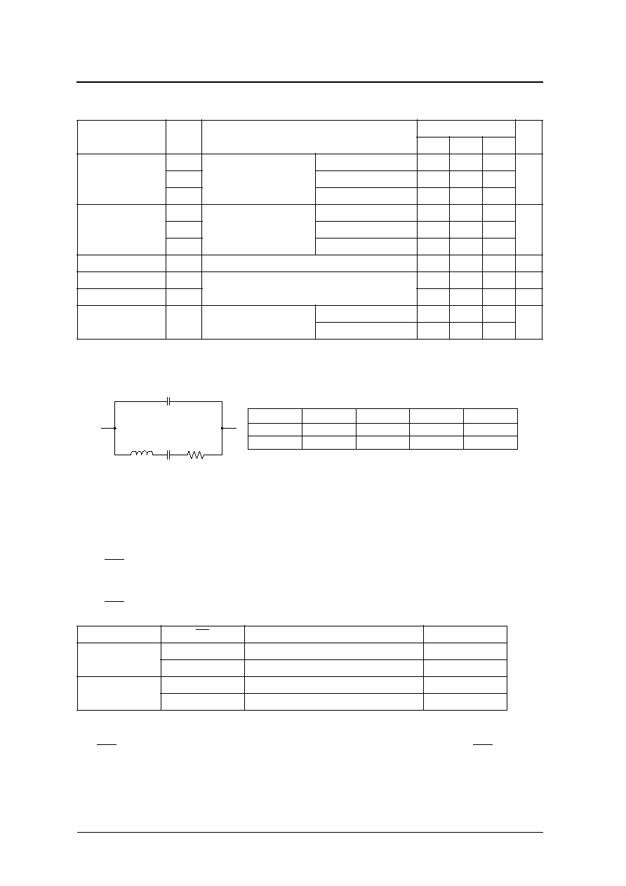
5009AN/CN series
3 V operation: V
DD
= 2.7 to 3.3 V, V
SS
= 0 V, Ta =
-20 to 80 �C unless otherwise noted.
P arameter
S y m b o l
Condition
Rating
Unit
m i n
typ
m a x
HIGH-level output voltage
V
O H
Q: Measurement cct 1, I
O H
= 8 m A
S M 5 0 0 9 A N 1 S , C F 5 0 0 9 A N 1
S M 5 0 0 9 A N 2 S , C F 5 0 0 9 A N 2
2.2
�
�
V
S M 5 0 0 9 A N 3 S , C F 5 0 0 9 A N 3
S M 5 0 0 9 A N 4 S , C F 5 0 0 9 A N 4
S M 5 0 0 9 A N 5 S , C F 5 0 0 9 A N 5
S M 5 0 0 9 A N 6 S , C F 5 0 0 9 A N 6
S M 5 0 0 9 C N 1 S , C F 5 0 0 9 C N 1
S M 5 0 0 9 C N 2 S , C F 5 0 0 9 C N 2
2.1
�
�
L O W -level output voltage
V
O L
Q: Measurement cct 1, I
O L
= 8 m A
�
�
0.4
V
Output leakage current
I
Z
Q: Measurement cct 2, I N H = L O W , V
O H
= V
D D
�
�
1 0
� A
Q: Measurement cct 2, I N H = L O W , V
O L
= V
S S
�
�
1 0
HIGH-level input voltage
V
IH
I N H
2.0
�
�
V
L O W -level input voltage
V
IL
I N H
�
�
0.3
V
Current consumption
I
D D
I N H = open, Measurement cct 3,
load cct 2, C
L
= 15 p F,
40 MHz cr ystal oscillator
S M 5 0 0 9 A N 1 S , C F 5 0 0 9 A N 1
�
8
1 7
m A
S M 5 0 0 9 A N 2 S , C F 5 0 0 9 A N 2
�
5
1 1
S M 5 0 0 9 A N 3 S , C F 5 0 0 9 A N 3
�
4
9
S M 5 0 0 9 A N 4 S , C F 5 0 0 9 A N 4
�
3
7
S M 5 0 0 9 A N 5 S , C F 5 0 0 9 A N 5
�
3
6
S M 5 0 0 9 A N 6 S , C F 5 0 0 9 A N 6
�
2
5
I N H = open, Measurement cct 3,
load cct 2, C
L
= 15 p F,
30 MHz cr ystal oscillator,
Ta = �10 to +70
�C
S M 5 0 0 9 C N 1 S , C F 5 0 0 9 C N 1
�
7
1 5
S M 5 0 0 9 C N 2 S , C F 5 0 0 9 C N 2
�
4
9
I N H pull-up resistance
R
U P
Measurement cct 4, V
D D
= 3 V, I N H = V
S S
4 0
�
2 0 0
k
Negative resistance
-R
L
V
D D
= 3 V, Ta = 25
�C, 40 M H z
�
� 1 0 0
�
F e e d b a ck resistance
R
f
Measurement cct 5
0.4
�
1.1
M
Built-in capacitance
C
G
Design value, determined by the internal wafer pattern
5.58
6
6.42
p F
C
D
9.3
1 0
10.7
p F
SM5009 series
NIPPON PRECISION CIRCUITS--10
5 V operation: V
DD
= 4.5 to 5.5 V, V
SS
= 0 V, Ta =
-
40 to 85
�
C unless otherwise noted.
P arameter
S y m b o l
Condition
Rating
Unit
m i n
typ
m a x
HIGH-level output voltage
V
O H
Q: Measurement cct 1, I
O H
= 16 m A
S M 5 0 0 9 A N 1 S , C F 5 0 0 9 A N 1
S M 5 0 0 9 A N 2 S , C F 5 0 0 9 A N 2
4.0
�
�
V
S M 5 0 0 9 A N 3 S , C F 5 0 0 9 A N 3
S M 5 0 0 9 A N 4 S , C F 5 0 0 9 A N 4
S M 5 0 0 9 A N 5 S , C F 5 0 0 9 A N 5
S M 5 0 0 9 A N 6 S , C F 5 0 0 9 A N 6
S M 5 0 0 9 C N 1 S , C F 5 0 0 9 C N 1
S M 5 0 0 9 C N 2 S , C F 5 0 0 9 C N 2
3.9
�
�
L O W -level output voltage
V
O L
Q: Measurement cct 1, I
O L
= 16 m A
�
�
0.4
V
Output leakage current
I
Z
Q: Measurement cct 2, I N H = L O W , V
O H
= V
D D
�
�
1 0
� A
Q: Measurement cct 2, I N H = L O W , V
O L
= V
S S
�
�
1 0
HIGH-level input voltage
V
IH
I N H
2.0
�
�
V
L O W -level input voltage
V
IL
I N H
�
�
0.8
V
Current consumption
I
D D
I N H = open, Measurement cct 3,
load cct 2, C
L
= 15 p F,
40 MHz cr ystal oscillator
C F 5 0 0 9 A N 1
�
1 2
2 6
m A
C F 5 0 0 9 A N 2
�
8
1 7
C F 5 0 0 9 A N 3
�
6
1 3
C F 5 0 0 9 A N 4
�
5
1 1
C F 5 0 0 9 A N 5
�
5
1 0
C F 5 0 0 9 A N 6
�
4
9
I N H = open, Measurement cct 3,
load cct 2, C
L
= 15 p F,
40 MHz cr ystal oscillator,
Ta = �20 to +80
�
C
S M 5 0 0 9 A N 1 S
�
1 2
2 6
S M 5 0 0 9 A N 2 S
�
8
1 7
S M 5 0 0 9 A N 3 S
�
6
1 3
S M 5 0 0 9 A N 4 S
�
5
1 1
S M 5 0 0 9 A N 5 S
�
5
1 0
S M 5 0 0 9 A N 6 S
�
4
9
I N H = open, Measurement cct 3,
load cct 2, C
L
= 15 p F,
30 MHz cr ystal oscillator
S M 5 0 0 9 C N 1 S , C F 5 0 0 9 C N 1
�
1 0
2 2
S M 5 0 0 9 C N 2 S , C F 5 0 0 9 C N 2
�
7
1 5
I N H pull-up resistance
R
U P
Measurement cct 4, V
D D
= 5 V, I N H = V
S S
4 0
�
2 0 0
k
Negative resistance
-
R
L
V
D D
= 5 V, Ta = 25
�
C , 40 M H z
�
� 2 1 0
�
F e e d b a ck resistance
R
f
Measurement cct 5
0.4
�
1.1
M
Built-in capacitance
C
G
Design value, determined by the internal wafer pattern
5.58
6
6.42
p F
C
D
9.3
1 0
10.7
p F
SM5009 series
NIPPON PRECISION CIRCUITS--11
Switching Characteristics
5009AH series
3 V operation: V
DD
= 2.7 to 3.3 V, V
SS
= 0 V, Ta =
-20 to 80 �C unless otherwise noted.
5 V operation: V
DD
= 4.5 to 5.5 V, V
SS
= 0 V, Ta =
-40 to 85 �C unless otherwise noted.
5009AK series
V
DD
= 4.5 to 5.5 V, V
SS
= 0 V, Ta =
-40 to 85 �C unless otherwise noted.
P arameter
S y m b o l
Condition
Rating
Unit
m i n
typ
m a x
Output rise time
t
r1
Measurement cct 3, load cct 2, 0.1V
D D
to 0.9V
D D
, C
L
= 15 p F
�
6
1 8
ns
Output fall time
t
f1
Measurement cct 3, load cct 2, 0.9V
D D
to 0.1V
D D
, C
L
= 15 p F
�
6
1 8
ns
Output duty cycle
1
1. Deter mined by the lot monitor.
Duty
Measurement cct 3, load cct 2, Ta = 25
�C, V
D D
= 3 V, C
L
= 15 p F
4 5
�
5 5
%
Output disable delay time
t
P L Z
Measurement cct 6, load cct 2, Ta = 25
�C, V
D D
= 3 V, C
L
15 pF
�
�
1 0 0
ns
Output enable delay time
t
P Z L
�
�
1 0 0
ns
M a x i m um operating
frequency
f
m a x
Measurement cct 3
1 6
�
�
M H z
P arameter
S y m b o l
Condition
Rating
Unit
m i n
typ
m a x
Output rise time
t
r1
Measurement cct 3, load cct 2, 0.1V
D D
to 0.9V
D D
, C
L
= 15 p F
�
4
1 2
ns
Output fall time
t
f1
Measurement cct 3, load cct 2, 0.9V
D D
to 0.1V
D D
, C
L
= 15 p F
�
4
1 2
ns
Output duty cycle
1
1. Deter mined by the lot monitor.
Duty
Measurement cct 3, load cct 2, Ta = 25
�C, V
D D
= 5 V, C
L
= 15 p F
4 5
�
5 5
%
Output disable delay time
t
P L Z
Measurement cct 6, load cct 2, Ta = 25
�C, V
D D
= 5 V, C
L
15 pF
�
�
1 0 0
ns
Output enable delay time
t
P Z L
�
�
1 0 0
ns
M a x i m um operating
frequency
f
m a x
Measurement cct 3
3 0
�
�
M H z
P arameter
S y m b o l
Condition
Rating
Unit
m i n
typ
m a x
Output rise time
t
r
Measurement cct 3, load cct 1, 0.4V to 2.4V, C
L
= 15 p F
�
2
6
ns
Output fall time
t
f
Measurement cct 3, load cct 1, 2.4V to 0.4V, C
L
= 15 p F
�
2
6
ns
Output duty cycle
1
1. Deter mined by the lot monitor.
Duty
Measurement cct 3, load cct 1, Ta = 25
�C, V
D D
= 5 V, C
L
= 15 p F
4 5
�
5 5
%
Output disable delay time
t
P L Z
Measurement cct 6, load cct 1, Ta = 25
�C, V
D D
= 5 V, C
L
15 pF
�
�
1 0 0
ns
Output enable delay time
t
P Z L
�
�
1 0 0
ns
M a x i m um operating
frequency
f
m a x
Measurement cct 3
Ta = �20 to +80
�C
4 0
�
�
M H z
Ta = �40 to +85
�C
3 0
�
�
SM5009 series
NIPPON PRECISION CIRCUITS--12
5009AL series
3 V operation: V
DD
= 2.7 to 3.3 V, V
SS
= 0 V, Ta =
-40 to 85 �C unless otherwise noted.
P arameter
S y m b o l
Condition
Rating
Unit
m i n
typ
m a x
Output rise time
t
r1
Measurement cct 3, load cct 2, 0.1V
D D
to 0.9V
D D
, C
L
= 15 p F
�
3.5
9
ns
Measurement cct 3, load cct 2, 0.1V
D D
to 0.9V
D D
,
V
D D
= 2.3 to 2.7 V, Ta = �20 to +80
�C, C
L
= 15 p F
�
4
1 3
t
r2
Measurement cct 3, load cct 2, 0.1V
D D
to 0.9V
D D
, C
L
= 30 p F
�
5
1 2
Measurement cct 3, load cct 2, 0.1V
D D
to 0.9V
D D
,
V
D D
= 2.3 to 2.7 V, Ta = �20 to +80
�C, C
L
= 30 p F
�
5.5
1 6
Output fall time
t
f1
Measurement cct 3, load cct 2, 0.9V
D D
to 0.1V
D D
, C
L
= 15 p F
�
3.5
9
ns
Measurement cct 3, load cct 2, 0.9V
D D
to 0.1V
D D
,
V
D D
= 2.3 to 2.7 V, Ta = �20 to +80
�C, C
L
= 15 p F
�
4
1 3
t
f2
Measurement cct 3, load cct 2, 0.9V
D D
to 0.1V
D D
, C
L
= 30 p F
�
5
1 2
Measurement cct 3, load cct 2, 0.9V
D D
to 0.1V
D D
,
V
D D
= 2.3 to 2.7 V, Ta = �20 to +80
�C, C
L
= 30 p F
�
5.5
1 6
Output duty cycle
1
1. Deter mined by the lot monitor.
Duty
Measurement cct 3, load cct 2, Ta = 25
�C, V
D D
= 3 V,
f
40 MHz, C
L
= 30 p F
4 5
�
5 5
%
Measurement cct 3, load cct 2, Ta = 25
�C, V
D D
= 2.4 V,
f
14.4 MHz, C
L
= 30 p F
4 0
�
6 0
C F 5 0 0 9 A L
� only, Measurement cct 3, load cct 2, Ta = 25 �C,
V
D D
= 2.5 V, f
30 MHz, C
L
= 15 p F
4 0
�
6 0
Output disable delay time
2
2. Oscillator stop function is built-in. W h e n I N H goes LOW , normal output stops. W h e n I N H goes HIGH, nor mal output is not resumed until after the
oscillator start-up time has elapsed.
t
P L Z
Measurement cct 6, load cct 2, Ta = 25
�C, V
D D
= 3 V, C
L
15 pF
�
�
1 0 0
ns
Output enable delay time
2
t
P Z L
�
�
1 0 0
ns
M a x i m um operating
frequency
f
m a x
Measurement cct 3
C F 5 0 0 9 A L
�
4 0
�
�
M H z
S M 5 0 0 9 A L
�S
3 0
�
�
Measurement cct 3, Ta = �20 to +80
�C
S M 5 0 0 9 A L
�S
4 0
�
�
Measurement cct 3, Ta = �20 to +80
�C
V
D D
= 2.4 to 2.7 V,
S M 5 0 0 9 A L
�S
14.4
�
�
V
D D
= 2.3 to 2.7 V,
C F 5 0 0 9 A L
�
3 0
�
�
V
D D
= 2.25 to 2.75 V,
C F 5 0 0 9 A L
�
2 0
�
�
SM5009 series
NIPPON PRECISION CIRCUITS--13
5 V operation: V
DD
= 4.5 to 5.5 V, V
SS
= 0 V, Ta =
-40 to 85 �C unless otherwise noted.
P arameter
S y m b o l
Condition
Rating
Unit
m i n
typ
m a x
Output rise time
t
r1
Measurement cct 3, load cct 2,
0.1V
D D
to 0.9V
D D
C
L
= 15 p F
�
2
4
ns
t
r2
C
L
= 30 p F
�
3.5
7
t
r3
C
L
= 50 p F
�
4
8
Output fall time
t
f1
Measurement cct 3, load cct 2,
0.9V
D D
to 0.1V
D D
C
L
= 15 p F
�
2
4
ns
t
f2
C
L
= 30 p F
�
3.5
7
t
f3
C
L
= 50 p F
�
4
8
Output duty cycle
1
1. Deter mined by the lot monitor.
Duty
Measurement cct 3, load cct 2, Ta = 25
�C, V
D D
= 5 V, C
L
= 50 p F
4 5
�
5 5
%
Output disable delay time
2
2. Oscillator stop function is built-in. W h e n I N H goes LOW , normal output stops. W h e n I N H goes HIGH, nor mal output is not resumed until after the
oscillator start-up time has elapsed.
t
P L Z
Measurement cct 6, load cct 2, Ta = 25
�C, V
D D
= 5 V, C
L
15 pF
�
�
1 0 0
ns
Output enable delay time
2
t
P Z L
�
�
1 0 0
ns
M a x i m um operating
frequency
f
m a x
Measurement cct 3
C F 5 0 0 9 A L
�
4 0
�
�
M H z
S M 5 0 0 9 A L
�S
3 0
�
�
Measurement cct 3, Ta = �20 to +80
�C
S M 5 0 0 9 A L
�S
4 0
�
�
SM5009 series
NIPPON PRECISION CIRCUITS--14
5009AN/CN series
3 V operation: V
DD
= 2.7 to 3.3 V, V
SS
= 0 V, Ta =
-20 to 80 �C unless otherwise noted.
P arameter
S y m b o l
Condition
Rating
Unit
m i n
typ
m a x
Output rise time
t
r1
Measurement cct 3, load cct 2,
0.1V
D D
to 0.9V
D D
,C
L
= 15 p F
S M 5 0 0 9 A N 1 S , C F 5 0 0 9 A N 1
S M 5 0 0 9 A N 2 S , C F 5 0 0 9 A N 2
�
3.5
9
ns
S M 5 0 0 9 A N 3 S , C F 5 0 0 9 A N 3
S M 5 0 0 9 A N 4 S , C F 5 0 0 9 A N 4
S M 5 0 0 9 A N 5 S , C F 5 0 0 9 A N 5
S M 5 0 0 9 A N 6 S , C F 5 0 0 9 A N 6
S M 5 0 0 9 C N 1 S , C F 5 0 0 9 C N 1
S M 5 0 0 9 C N 2 S , C F 5 0 0 9 C N 2
�
5
1 3
t
r2
Measurement cct 3, load cct 2,
0.1V
D D
to 0.9V
D D
,C
L
= 30 p F
S M 5 0 0 9 A N 1 S , C F 5 0 0 9 A N 1
S M 5 0 0 9 A N 2 S , C F 5 0 0 9 A N 2
�
5
1 2
S M 5 0 0 9 A N 3 S , C F 5 0 0 9 A N 3
S M 5 0 0 9 A N 4 S , C F 5 0 0 9 A N 4
S M 5 0 0 9 A N 5 S , C F 5 0 0 9 A N 5
S M 5 0 0 9 A N 6 S , C F 5 0 0 9 A N 6
S M 5 0 0 9 C N 1 S , C F 5 0 0 9 C N 1
S M 5 0 0 9 C N 2 S , C F 5 0 0 9 C N 2
�
7
1 6
Output fall time
t
f1
Measurement cct 3, load cct 2,
0.9V
D D
to 0.1V
D D
,C
L
= 15 p F
S M 5 0 0 9 A N 1 S , C F 5 0 0 9 A N 1
S M 5 0 0 9 A N 2 S , C F 5 0 0 9 A N 2
�
3.5
9
ns
S M 5 0 0 9 A N 3 S , C F 5 0 0 9 A N 3
S M 5 0 0 9 A N 4 S , C F 5 0 0 9 A N 4
S M 5 0 0 9 A N 5 S , C F 5 0 0 9 A N 5
S M 5 0 0 9 A N 6 S , C F 5 0 0 9 A N 6
S M 5 0 0 9 C N 1 S , C F 5 0 0 9 C N 1
S M 5 0 0 9 C N 2 S , C F 5 0 0 9 C N 2
�
5
1 3
t
f2
Measurement cct 3, load cct 2,
0.9V
D D
to 0.1V
D D
,C
L
= 30 p F
S M 5 0 0 9 A N 1 S , C F 5 0 0 9 A N 1
S M 5 0 0 9 A N 2 S , C F 5 0 0 9 A N 2
�
5
1 2
S M 5 0 0 9 A N 3 S , C F 5 0 0 9 A N 3
S M 5 0 0 9 A N 4 S , C F 5 0 0 9 A N 4
S M 5 0 0 9 A N 5 S , C F 5 0 0 9 A N 5
S M 5 0 0 9 A N 6 S , C F 5 0 0 9 A N 6
S M 5 0 0 9 C N 1 S , C F 5 0 0 9 C N 1
S M 5 0 0 9 C N 2 S , C F 5 0 0 9 C N 2
�
7
1 6
Output duty cycle
1
1. Deter mined by the lot monitor.
Duty
Measurement cct 3, load cct 2,
Ta = 25
�C, V
D D
= 3 V
C
L
= 30 p F,
S M 5 0 0 9 A N
�S, CF5009AN�
4 5
�
5 5
%
C
L
= 15 p F,
S M 5 0 0 9 C N
�S, CF5009CN�
4 0
�
6 0
Output disable delay time
t
P L Z
Measurement cct 6, load cct 2, Ta = 25
�C, V
D D
= 3 V, C
L
15 pF
�
�
1 0 0
ns
Output enable delay time
t
P Z L
�
�
1 0 0
ns
M a x i m um operating
frequency
f
m a x
Measurement cct 3
S M 5 0 0 9 A N
�S, CF5009AN�
4 0
�
�
M H z
Ta = �10 to +70
�C,
S M 5 0 0 9 C N
�S, CF5009CN�
3 0
�
�
SM5009 series
NIPPON PRECISION CIRCUITS--15
5 V operation: V
DD
= 4.5 to 5.5 V, V
SS
= 0 V, Ta =
-40 to 85 �C unless otherwise noted.
Current consumption and Output waveform with NPC's standard crystal
FUNCTIONAL DESCRIPTION
Standby Function
AH, AK, AN, CN series
When INH goes LOW, the output on Q becomes high impedance, but internally the oscillator does not stop.
AL series
When INH goes LOW, the oscillator stops and the oscillator output on Q becomes high impedance.
Power-save Pull-up Resistance (AL series only)
The INH pull-up resistance changes in response to the input level (HIGH or LOW). When INH goes LOW
(standby state), the pull-up resistance becomes large to reduce the current consumption during standby.
P arameter
S y m b o l
Condition
Rating
Unit
m i n
typ
m a x
Output rise time
t
r1
Measurement cct 3, load cct 2,
0.1V
D D
to 0.9V
D D
C
L
= 15 p F
�
2
4
ns
t
r2
C
L
= 30 p F
�
3.5
7
t
r3
C
L
= 50 p F
�
4
8
Output fall time
t
f1
Measurement cct 3, load cct 2,
0.9V
D D
to 0.1V
D D
C
L
= 15 p F
�
2
4
ns
t
f2
C
L
= 30 p F
�
3.5
7
t
f3
C
L
= 50 p F
�
4
8
Output duty cycle
1
1. Deter mined by the lot monitor.
Duty
Measurement cct 3, load cct 2, Ta = 25
�C, V
D D
= 5 V, C
L
= 50 p F
4 5
�
5 5
%
Output disable delay time
t
P L Z
Measurement cct 6, load cct 2, Ta = 25
�C, V
D D
= 5 V, C
L
15 pF
�
�
1 0 0
ns
Output enable delay time
t
P Z L
�
�
1 0 0
ns
M a x i m um operating
frequency
f
m a x
Measurement cct 3
C F 5 0 0 9 A N
�, SM5009AN�S
4 0
�
�
M H z
S M 5 0 0 9 C N
�S, CF5009CN�
3 0
�
�
V ersion
I N H
Q
Oscillator
AH, AK, AN, CN series
HIGH (or open)
A n y f
O
, f
O
/2, f
O
/4, f
O
/8, f
O
/16 or f
O
/32 output frequency
N o r mal operation
L O W
High impedance
N o r mal operation
AL series
HIGH (or open)
A n y f
O
, f
O
/2, f
O
/4, f
O
/8, f
O
/16 or f
O
/32 output frequency
N o r mal operation
L O W
High impedance
Stopped
f (MHz)
R (
)
L (mH)
Ca (fF)
Cb (pF)
30
17.2
4.36
6.46
2.26
40
16.8
2.90
5.47
2.08
L
Ca
R
Cb
SM5009 series
NIPPON PRECISION CIRCUITS--16
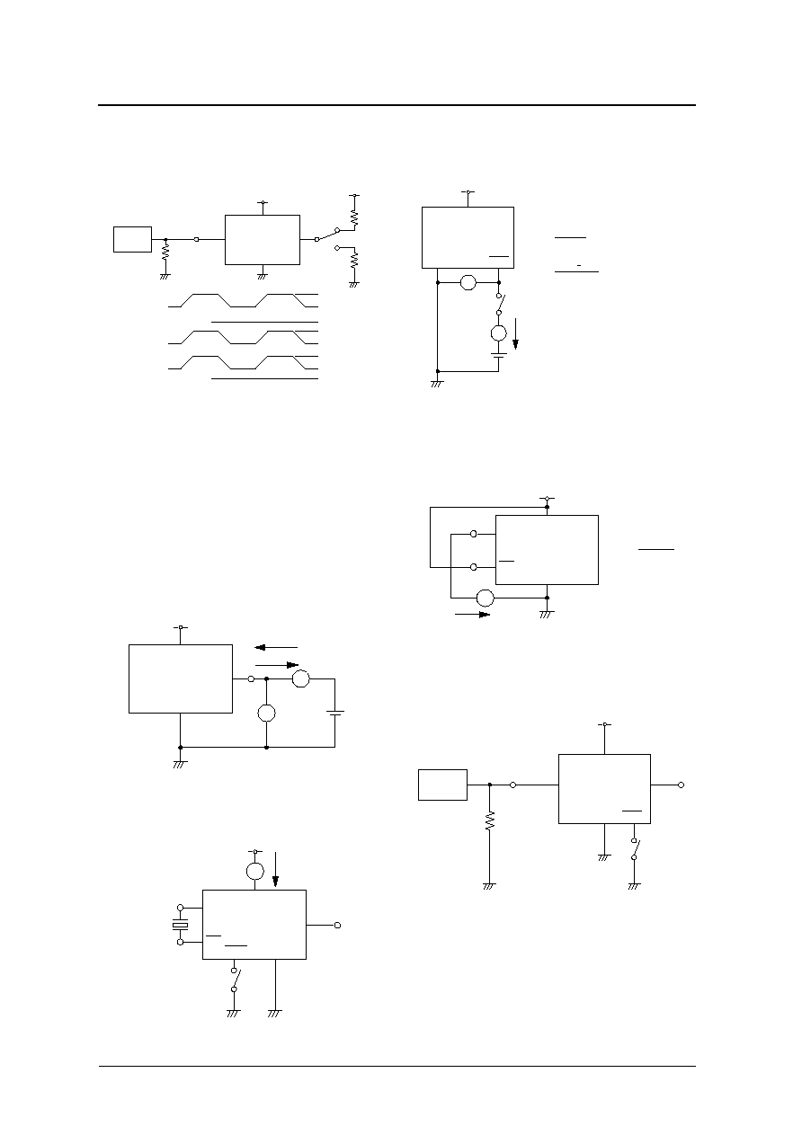
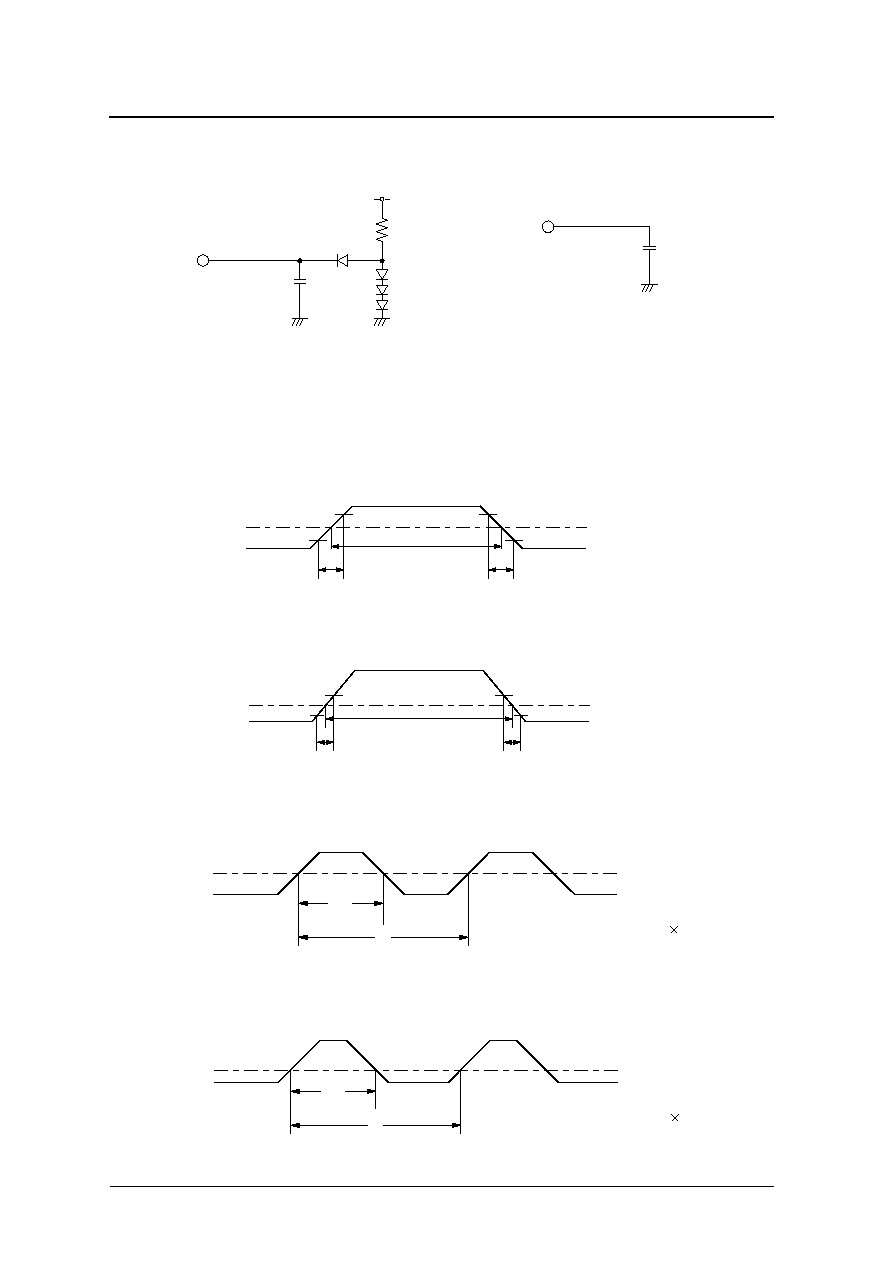
MEASUREMENT CIRCUITS
Measurement cct 1
� 5009AK�, AL�, AN1, AN2
R1 : 50
R2 : 250
(V
D D
= 4.5V), 275(V
D D
= 2.7V)
R3 : 256
(V
D D
= 4.5V), 288(V
D D
= 2.7V)
� 5009AN3 to AN6, CN�
R1 : 50
R2 : 245
(V
D D
= 4.5V), 262(V
D D
= 2.7V)
R3 : 256
(V
D D
= 4.5V), 288(V
D D
= 2.7V)
� 5009AH�
R1 : 50
R2 : 1000
(V
D D
= 4.5V), 1100(V
D D
= 2.7V)
R3 : 1025
(V
D D
= 4.5V), 1150(V
D D
= 2.7V)
Measurement cct 2
Measurement cct 3
Signal
Generator
VDD
VSS
XT
Q
R1
R2
R3
V
DD
0V
XT input waveform
(10MHz)
V
OH
0V
Q output
V
DD
V
DD
V
OL
Q output
0V
When
measuring
V
OL
When
measuring
V
OH
VDD
VSS
Q
I
Z
V
OH
V
OL
V
A
I
Z
VDD
VSS
XT
Q
X'tal
XT
INH
I
DD
I
ST
A
Measurement cct 4
Measurement cct 5
Measurement cct 6
R1 : 50
VDD
VSS
I
PR
A
3.0V or 5.0V
INH
V
V
IH
V
IL
V
DD
I
PR
(V
IL
= 0V)
R
UP2
=
I
PR
V
IH
: 2.1V(V
DD
= 3.0V)
V
IH
: 3.5V(V
DD
= 5.0V)
V
DD
V
IH
R
UP
R
UP1
=
VDD
VSS
I
Rf
R
f
=
XT
V
DD
I
Rf
XT
A
Signal
Generator
VSS
XT
Q
R1
VDD
INH
SM5009 series
NIPPON PRECISION CIRCUITS--17
Load cct 1
Load cct 2
Switching Time Measurement Waveform
Output duty level (CMOS)
Output duty level (TTL)
Output duty cycle (CMOS)
Output duty cycle (TTL)
C
L
= 15pF : D U T Y , I
D D
, t
r
, t
f
R = 400
Q output
(Including proove
capacitance)
R
C
L
C
L
= 15pF : D U T Y , I
D D
, t
r1
, t
f1
C
L
= 30pF : t
r2
, t
f2
C
L
= 50pF : t
r3
, t
f3
Q output
(Including probe
capacitance)
C
L
0.9V
DD
0.1V
DD
0.9V
DD
0.1V
DD
t
r
t
f
Q output
DUTY measurement
voltage (0.5V
DD
)
T
W
2.4V
0.4V
2.4V
0.4V
t
r
t
f
Q output
DUTY measurement
voltage (1.4V
)
T
W
DUTY measurement
voltage
(
0.5V
DD
)
Q output
T
W
T
DUTY= T
W
/ T 100 (%)
DUTY measurement
voltage
(
1.4V
)
Q output
T
W
T
DUTY= T
W
/ T 100 (%)
NIPPON PRECISION CIRCUITS INC. reserves the right to make changes to the products described in this data sheet in order to
improve the design or performance and to supply the best possible products. Nippon Precision Circuits Inc. assumes no responsibility for
the use of any circuits shown in this data sheet, conveys no license under any patent or other rights, and makes no claim that the circuits
are free from patent infringement. Applications for any devices shown in this data sheet are for illustration only and Nippon Precision
Circuits Inc. makes no claim or warranty that such applications will be suitable for the use specified without fur ther testing or modification.
The products described in this data sheet are not intended to use for the apparatus which influence human lives due to the failure or
malfunction of the products. Customers are requested to comply with applicable laws and regulations in effect now and hereinafter,
including compliance with expor t controls on the distribution or dissemination of the products. Customers shall not expor t, directly or
indirectly, any products without first obtaining required licenses and approvals from appropriate government agencies.
NIPPON PRECISION CIRCUITS INC.
4-3, Fukuzumi 2-chome
Koto-ku, Tokyo 135-8430, Japan
Telephone: 03-3642-6661
Facsimile: 03-3642-6698
SM5009 series
NIPPON PRECISION CIRCUITS--18
NC9801FE
2000.09
NIPPON PRECISION CIRCUITS INC.
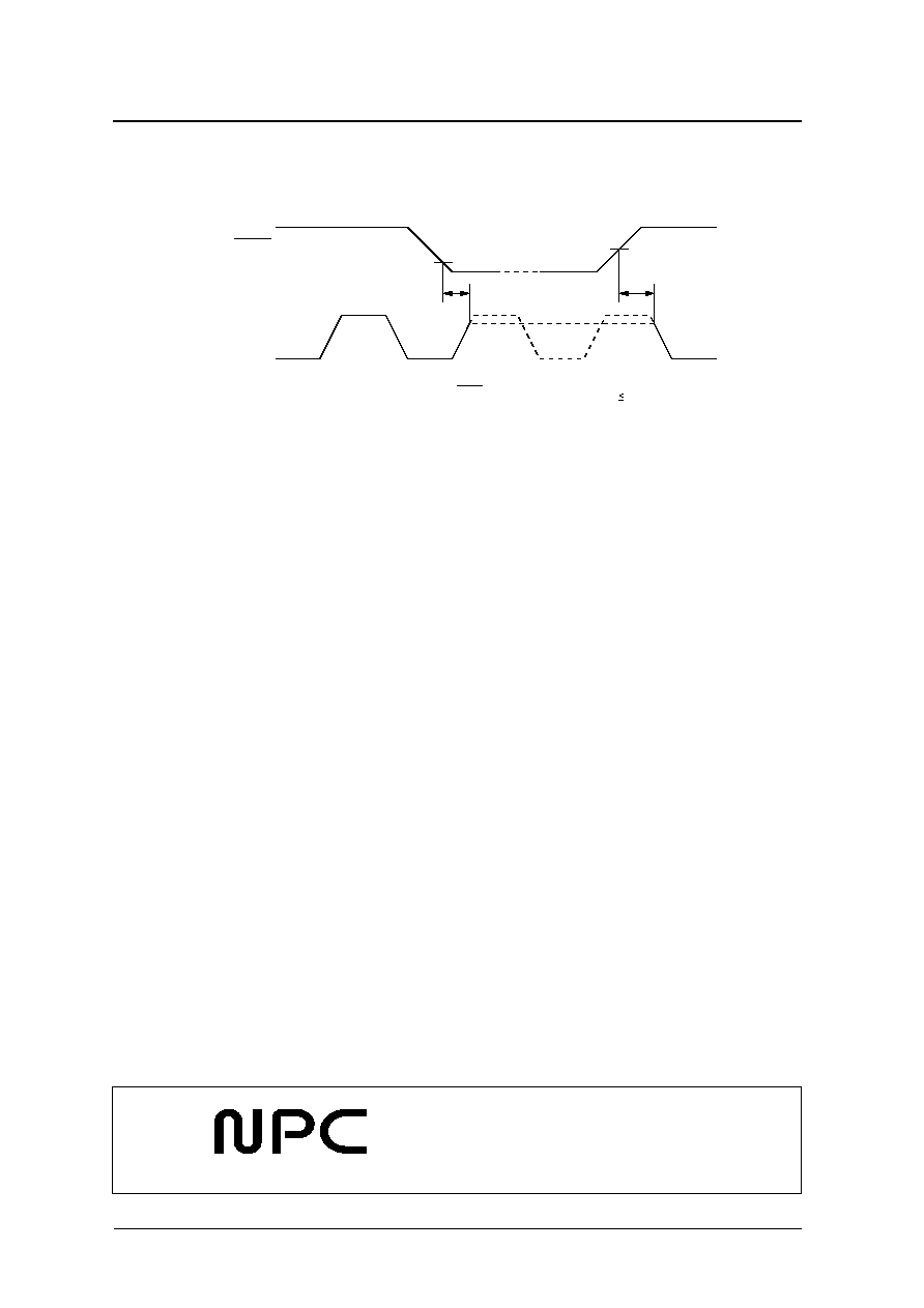
Output Enable/Disable Delay
Note (AL series only) : when the device is in standby, the oscillator stops. When standby is released, the oscil-
lator starts and stable oscillator output occurs after a short delay.
Q output
INH
V
IH
V
IL
t
PLZ
t
PZL
INH input waveform
t
r =
t
f 10ns