SM5009 series
NIPPON PRECISION CIRCUITS INC.--1
Crystal Oscillator Module ICs
OVERVIEW
The SM5009 series are crystal oscillator module ICs that incorporate low crystal current type oscillating circuit
to limit oscillator-stage current, so that they can reduce crystal current lower than the existing products. Since
the oscillating circuit has oscillator capacitors with excellent frequency response and feedback resistor built-in,
just connecting crystal realizes stable fundamental oscillation responding up to 40MHz. The SM5009 series
are ideal for SMD type crystal oscillator using a strip-shaped crystal blank.
FEATURES
I
Low crystal current oscillator
I
Up to 40MHz operating frequency range (funda-
mental oscillation)
I
Operating supply voltage range
∑ 3V operation: 2.7 to 3.6V
∑ 5V operation: 4.5 to 5.5V
I
≠40 to 85
∞
C operating temperature range
I
Oscillation capacitors C
G
, C
D
built-in
I
Inverter amplifier feedback resistor built-in
I
Standby function
∑ Oscillator stops (AL series), high impedance in
standby mode
I
Low standby current
∑ Power-save pull-up resistor built-in (AL series)
I
Frequency divider built-in (f
O
, f
O
/2, f
O
/4, f
O
/8,
f
O
/16, f
O
/32 determined by internal connection)
I
Output drive capability
∑ AL
◊
, AN
◊
, AK
◊
, CN
◊
: 16mA (V
DD
=
4.5V)
∑ AH
◊
: 4mA (V
DD
=
4.5V)
I
Output load: C
L
= 50pF max.
I
Output duty level
∑ CMOS level (1/2 VDD): AL
◊
, AN
◊
, AH
◊
, CN
◊
∑ TTL level (1.4V): AK
◊
I
Molybdenum-gate CMOS process
I
8-pin SOP (SM5009
◊◊◊
S)
I
Chip form (CF5009
◊◊◊
)
SERIES CONFIGURATION
APPLICATIONS
I
SMD type crystal oscillator module
ORDERING INFORMATION
Version
1
1. Package devices (8-pin SOP) have designation SM5009
◊◊◊
S.
3V operation
5V operation
Output
duty level
Output
frequency
INH Input
level
Standby mode
Recommended
operating
frequency
range
2
[MHz]
2. The recommended operating frequency is a yardstick value derived from the crystal used for NPC characteristics authentication. However, the oscil-
lator frequency band is not guaranteed. Specifically, the characteristics can vary greatly due to crystal characteristics and mounting conditions, so
the oscillation characteristics of components must be carefully evaluated.
Output
load
3
(max)
[pF]
3. Output load value is the maximum load capacitance that allows drive.
Recommended
operating
frequency
range
2
[MHz]
Output
load
3
(max)
[pF]
Oscillator
stop
function
Output
state
CF5009AL1
Up to 40
50
Up to 40
50
CMOS
f
O
CMOS
Yes
Hi-Z
CF5009AL2
f
O
/2
CF5009AL3
f
O
/4
CF5009AL4
f
O
/8
CF5009AL5
f
O
/16
CF5009AL6
f
O
/32
CF5009AN1
Up to 40
30
Up to 40
50
CMOS
f
O
TTL
No
Hi-Z
CF5009AN2
f
O
/2
CF5009AN3
CMOS/TTL
f
O
/4
CF5009AN4
f
O
/8
CF5009AN5
f
O
/16
CF5009AN6
f
O
/32
CF5009CN1
Up to 30
15
Up to 30
50
CMOS
f
O
TTL
No
Hi-Z
CF5009CN2
f
O
/2
CF5009AK1
≠
≠
Up to 40
15
TTL
f
O
TTL
No
Hi-Z
CF5009AK2
f
O
/2
CF5009AH1
Up to 16
15
Up to 30
15
CMOS
f
O
TTL
No
Hi-Z
CF5009AH2
f
O
/2
CF5009AH3
f
O
/4
CF5009AH4
f
O
/8
Device
Package
SM5009
◊◊◊
S
8-pin SOP
CF5009
◊◊◊
≠1
Chip form
SM5009 series
NIPPON PRECISION CIRCUITS INC.--2
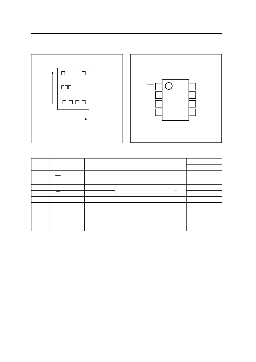
PAD LAYOUT
(Unit:
µ
m)
PINOUT
(Top view)
PIN DESCRIPTION and PAD DIMENSIONS
Chip size: 0.92
◊
1.22 mm
Chip thickness: 300 ± 30 µm
Chip base: V
DD
level
Q
VDD
XT
VSS
(0,0)
(920,1220)
X
Y
HA5009
INH
XT
1
XT
VSS
Q
VDD
4
2
3
NC
NC
8
7
6
5
XT
INH
Number
Name
I/O
Description
Pad dimensions [µm]
X
Y
1
INH
I
Output state control input. Standby mode when LOW, pull-up resistor built-in.
In the case of the CF5009AL
◊
, the oscillator stops and power-save pull-up
resistor built in to reduce current consumption at standby mode.
195
212
2
XT
I
Amplifier input.
Crystal oscillator connection pins.
Crystal oscillator connected between XT and XT
385
212
3
XT
O
Amplifier output.
575
212
4
VSS
≠
Ground
766
212
5
Q
O
Output. Output frequency (f
O
, f
O
/2, f
O
/4, f
O
/8, f
O
/16, f
O
/32) determined by
internal connection
765
1062
6
NC
≠
No connection
≠
≠
7
NC
≠
No connection
≠
≠
8
VDD
≠
Supply voltage
162
1062

SM5009 series
NIPPON PRECISION CIRCUITS INC.--3
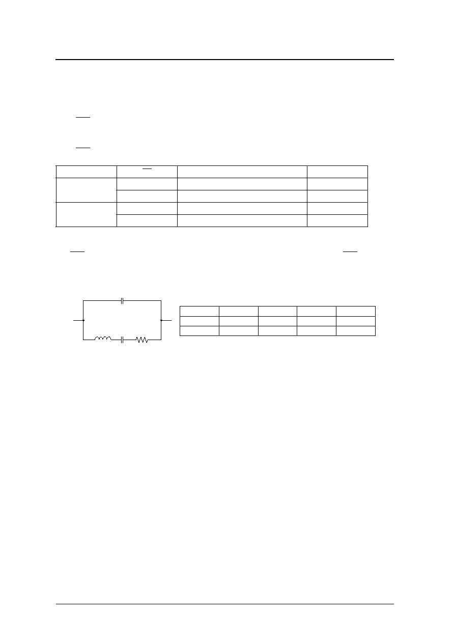
PACKAGE DIMENSIONS
(Unit: mm)
∑
8-pin SOP
BLOCK DIAGRAM
Notes. The SM5009 series reduce crystal current by limiting driving current of oscillating-stage inverter and inhibiting oscillating amplitude. Depending on
the characteristics of using crystal or the mounting condition, they may not oscillate normally. Please evaluate the oscillation start-up characteris-
tics adequately with your actual device.
4.4 0.2
1.5 0.1
0.05 0.05
0.4 0.2
5.2 0.3
0.4 0.1
0.15
+ 0.1
- 0.05
0 to 10
6.2 0.3
0.695typ
1.27
0.12
M
0.10
XT
VSS
VDD
Q
C
Gp
C
Dp
R
f
XT
INH
1/2
1/2
1/2
1/2
1/2
C
Gn
C
Dn
SM5009 series
NIPPON PRECISION CIRCUITS INC.--4
FUNCTIONAL DESCRIPTION
Standby Function
5009 AL
◊
series
When INH goes LOW, the oscillator stops and the oscillator output on Q becomes high impedance.
5009AH
◊
, AK
◊
, AN
◊
, CN
◊
series
When INH goes LOW, the output on Q becomes high impedance, but internally the oscillator does not stop.
Power-save Pull-up Resistance (AL
◊
series only)
The INH pull-up resistance changes in response to the input level (HIGH or LOW). When INH goes LOW
(standby state), the pull-up resistance becomes large to reduce the current consumption during standby.
Current consumption and Output waveform with NPC's standard crystal
Version
INH
Q
Oscillator
AL
◊
series
HIGH (or open)
Any f
O
, f
O
/2, f
O
/4, f
O
/8, f
O
/16 or f
O
/32 output frequency
Normal operation
LOW
High impedance
Stopped
AH
◊
, AK
◊
, AN
◊
, CN
◊
series
HIGH (or open)
Any f
O
, f
O
/2, f
O
/4, f
O
/8, f
O
/16 or f
O
/32 output frequency
Normal operation
LOW
High impedance
Normal operation
f [MHz]
R [
]
L [mH]
Ca [fF]
Cb [pF]
30
17.2
4.36
6.46
2.26
40
16.8
2.90
5.47
2.08
L
Ca
R
Cb
SM5009 series
NIPPON PRECISION CIRCUITS INC.--5
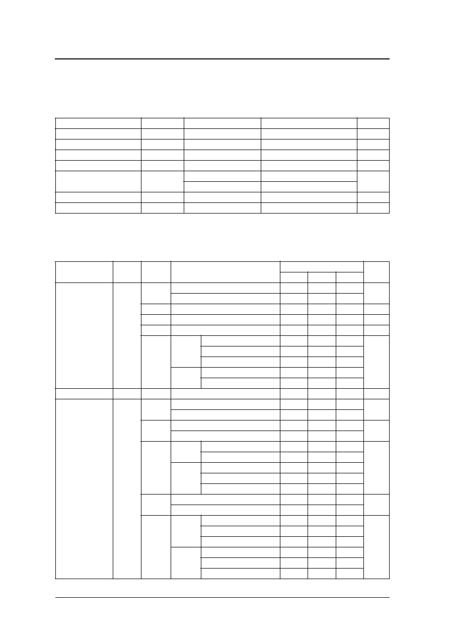
SPECIFICATIONS
Absolute Maximum Ratings
V
SS
= 0V unless otherwise noted.
Recommended Operating Conditions
V
SS
= 0V unless otherwise noted.
Parameter
Symbol
Condition
Rating
Unit
Supply voltage range
V
DD
-
0.5 to +7.0
V
Input voltage range
V
IN
-
0.5 to V
DD
+ 0.5
V
Output voltage range
V
OUT
-0.5 to V
DD
+ 0.5
V
Operating temperature range
T
opr
-40 to +85
∞C
Storage temperature range
T
stg
Chip form
-65 to +150
∞C
8-pin SOP
-55 to +125
Output current
I
OUT
25
mA
Power dissipation
P
D
8-pin SOP
500
mW
Parameter
Symbol
Version
Condition
Rating
Unit
min
typ
max
Supply voltage
V
DD
AH
◊
f
30MHz
4.5
≠
5.5
V
f
16MHz
2.7
≠
3.3
AK
◊
f
40MHz
4.5
≠
5.5
V
AN
◊
f
40MHz
2.7
≠
5.5
V
CN
◊
f
30MHz
2.7
≠
5.5
V
AL
◊
Chip form
f
40MHz
2.7
≠
5.5
V
f
30MHz
2.3
≠
2.7
f
20MHz
2.25
≠
2.75
8-pin SOP
f
40MHz
2.7
≠
5.5
f
14.4MHz
2.4
≠
2.7
Input voltage
V
IN
All version
V
SS
≠
V
DD
V
Operating temperature
T
OPR
AH
◊
f
30MHz, 4.5V V
DD
5.5V
- 40
≠
+ 85
∞C
f
16MHz, 2.7V V
DD
3.6V
- 20
≠
+ 80
AK
◊
f
30MHz
- 40
≠
+ 85
∞C
30MHz
< f 40MHz
- 20
≠
+ 80
AN
◊
Chip form
f
40MHz, 2.7V V
DD
< 4.5V
- 20
≠
+ 80
∞C
f
40MHz, 4.5V V
DD
5.5V
- 40
≠
+ 85
8-pin SOP
f
40MHz, 2.7V V
DD
< 4.5V
- 20
≠
+ 80
f
40MHz, 4.5V V
DD
5.5V
- 20
≠
+ 80
f
30MHz, 4.5V V
DD
5.5V
- 40
≠
+ 85
CN
◊
f
30MHz, 2.7V V
DD
< 4.5V
- 10
≠
+ 70
∞C
f
30MHz, 4.5V V
DD
5.5V
- 40
≠
+ 85
AL
◊
Chip form
f
40MHz, 2.7V V
DD
5.5V
- 40
≠
+ 85
∞C
f
30MHz, 2.3V V
DD
2.7V
- 20
≠
+ 80
f
20MHz, 2.25V V
DD
2.75V
- 20
≠
+ 80
8-pin SOP
f
40MHz, 2.7V V
DD
5.5V
- 20
≠
+ 80
f
30MHz, 2.7V V
DD
5.5V
- 40
≠
+ 85
f
14.4MHz, 2.4V V
DD
2.7V
- 20
≠
+ 80