 | –≠–ª–µ–∫—Ç—Ä–æ–Ω–Ω—ã–π –∫–æ–º–ø–æ–Ω–µ–Ω—Ç: SM58852 | –°–∫–∞—á–∞—Ç—å:  PDF PDF  ZIP ZIP |
DECO SM588
◊
series
NIPPON PRECISION CIRCUITS--1
NIPPON PRECISION CIRCUITS INC.
Audio 3rd-order
D/A Converter
OVERVIEW
The
DECO SM588
◊
series, fabricated using NPC's Molybdenum-gate CMOS process, are D/A converter ICs
for digital audio, that provide all the basic converter functions in miniature 8-pin packages. They each feature
built-in 8-times oversampling digital filter,
jitter-compensated D/A converter, and post-analog lowpass fil-
ter converter stages required for digital audio. They can sample at up to 96kHz for 16 or 24-bit input word
length. A type with built-in deemphasis filter is also available for applications requiring deemphasis.
FEATURES
3-wire Input
I
2-channel stereo configuration
I
256fs, 384fs, or 512fs system clock (applied by
product / version)
I
Input format
3-wire serial, MSB first, rear-packed
16 or 24-bit (applied by product / version)
I
8-times oversampling digital filter
∑ 32 dB stopband attenuation
∑ ±0.05 dB passband ripple
I
2-channel D/A converter
∑ 3rd-order noise shaper
∑ Oversampling operation
I
3rd-order post-analog lowpass filter
I
4.5 to 5.5 V supply voltage
I
8-pin SOP
I
Molybdenum-gate CMOS process
2-wire Input with Deemphasis Filter
I
2-channel stereo configuration
I
256fs, 384fs, or 512fs system clock (applied by
product / version)
I
Input format
2-wire serial, MSB first, rear-packed
16 or 24-bit (applied by product / version)
I
Deemphasis filter (fs = 44.1 kHz sample rate)
I
8-times oversampling digital filter
∑ 32 dB stopband attenuation
∑ ±0.05 dB passband ripple
I
2-channel D/A converter
∑ 3rd-order noise shaper
∑ Oversampling operation
I
3rd-order post-analog lowpass filter
I
4.5 to 5.5 V supply voltage
I
8-pin SOP
I
Molybdenum-gate CMOS process
APPLICATIONS
I
Audio equipment
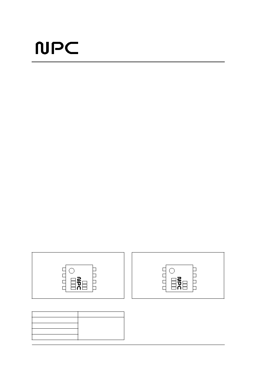
PINOUTS
ORDERING INFORMATION
3-wire input
2-wire input with built-in deemphasis filter
DATA
BCKI
LRCI
CLK
LO
VDD
VSS
RO
1
4
5
8
5
88
1
4
5
8
DATA
DEEM
LRCI
CLK
LO
VDD
VSS
RO
5
88
Device
Package
SM5882AS
8-pin SOP
SM5883AS
SM5883BS
SM5885CS
SM588
◊
series
NIPPON PRECISION CIRCUITS--2
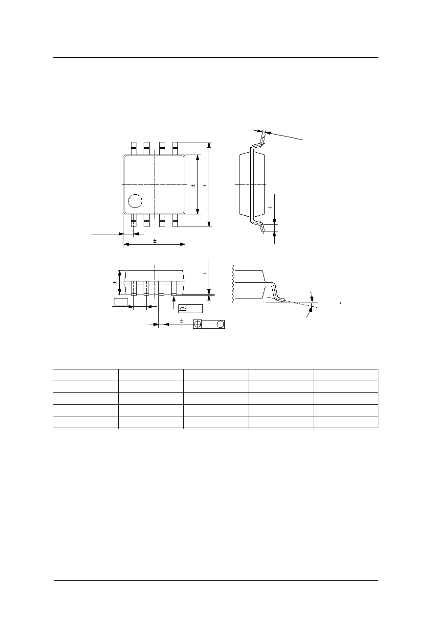
PACKAGE DIMENSIONS
(Unit : mm)
Weight : 0.07g
SERIES LINEUP
Device
Input length
Type
Pin 2 function
Master clock
SM5882AS
16
2-wire input
Deemphasis control
384fs
SM5883AS
16
3-wire input
Bit clock input
384fs
SM5883BS
16
3-wire input
Bit clock input
256fs
SM5885CS
24
3-wire input
Bit clock input
512fs
4.4 0.2
1.5 0.1
0.05 0.05
0.4 0.2
5.2 0.3
0.4 0.1
0.15
+ 0.1
- 0.05
0 to 10
6.2 0.3
0.695typ
1.27
0.12
M
0.10
SM588
◊
series
NIPPON PRECISION CIRCUITS--3
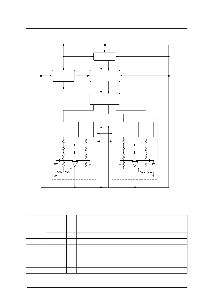
BLOCK DIAGRAM
PIN DESCRIPTION
Number
Name
I/O
Description
1
DATA
I
Serial data input
2
BCKI
1
1. 3-wire
type
I
Bit clock input
DEEM
2
2. 2-wire type with built-in deemphasis filter
I
Deemphasis ON/OFF control (44.1 kHz, ON when HIGH)
3
LRCI
I
Sample rate (fs) clock input. Left-channel input when HIGH, and right-channel input when LOW.
4
CLK
I
External clock input
5
RO
O
Right-channel analog output
6
VSS
≠
Ground
7
VDD
≠
Supply
8
LO
O
Left-channel analog output
Filter & attenuation
operation block
Noise shaper
operation block
Input interface
+
-
+
-
Timing
control
LRCI
DATA
BCKI*
LO
VSS
RO
CLK
DEEM**
L
R
L
R
VDD
9 Level
DEM DAC
9 Level
DEM DAC
9 Level
DEM DAC
9 Level
DEM DAC
* : Not available for 2-wire input type
** : Not available for 3-wire input type
SM588
◊
series
NIPPON PRECISION CIRCUITS--4
SPECIFICATIONS
Absolute Maximum Ratings
V
SS
= 0 V
Recommended Operating Conditions
V
SS
= 0 V
DC Characteristics
V
DD
= 4.5 to 5.5 V, V
SS
= 0 V, Ta =
-
40 to 85
∞
C
Parameter
Symbol
Rating
Unit
Supply voltage range
V
DD
-
0.3 to 7.0
V
Input voltage range
1
1. All inputs
Also applicable during supply switching.
V
IN
V
SS
-
0.3 to V
DD
+
0.3
V
Storage temperature range
T
STG
-
55 to 125
∞
C
Power dissipation
P
D
300
mW
Parameter
Symbol
Rating
Unit
Supply voltage
V
DD
4.5 to 5.5
V
Operating temperature
T
OPR
-
40 to 85
∞
C
Parameter
Symbol
Condition
Rating
Unit
min
typ
max
Current consumption
1
1. V
DD
= 5 V, CLK clock input frequency f
CLK
= 16.9344 MHz (384fs type)/11.2896 MHz (256fs type)/22.5792MHz (512fs type), no output load.
Input data: NPC pattern.
I
DD
≠
12.5
25.0
mA
CLK HIGH-level input voltage
V
IH1
Clock input
0.7V
DD
≠
≠
V
CLK LOW-level input voltage
V
IL1
Clock input
≠
≠
0.3V
DD
V
CLK AC-coupled input voltage
V
INAC
0.7
≠
≠
V
p-p
HIGH-level input voltage
2
2. Pins BCKI (3-wire type), DEEM (2-wire type with deemphasis filter), DATA, LRCI
V
IH2
0.5V
DD
≠
≠
V
LOW-level input voltage
2
V
IL2
≠
≠
0.2V
DD
V
CLK HIGH-level input current
I
IH
V
IN
= V
DD
20
62
170
µA
CLK LOW-level input current
I
IL
V
IN
= 0 V
20
62
170
µA
Input leakage current
2
I
LH
V
IN
= V
DD
≠
≠
1.0
µA
I
LL
V
IN
= 0 V
≠
≠
1.0
µA
SM588
◊
series
NIPPON PRECISION CIRCUITS--5
AC Digital Characteristics
V
DD
= 4.5 to 5.5 V, V
SS
= 0 V, Ta =
-
40 to 85
∞
C
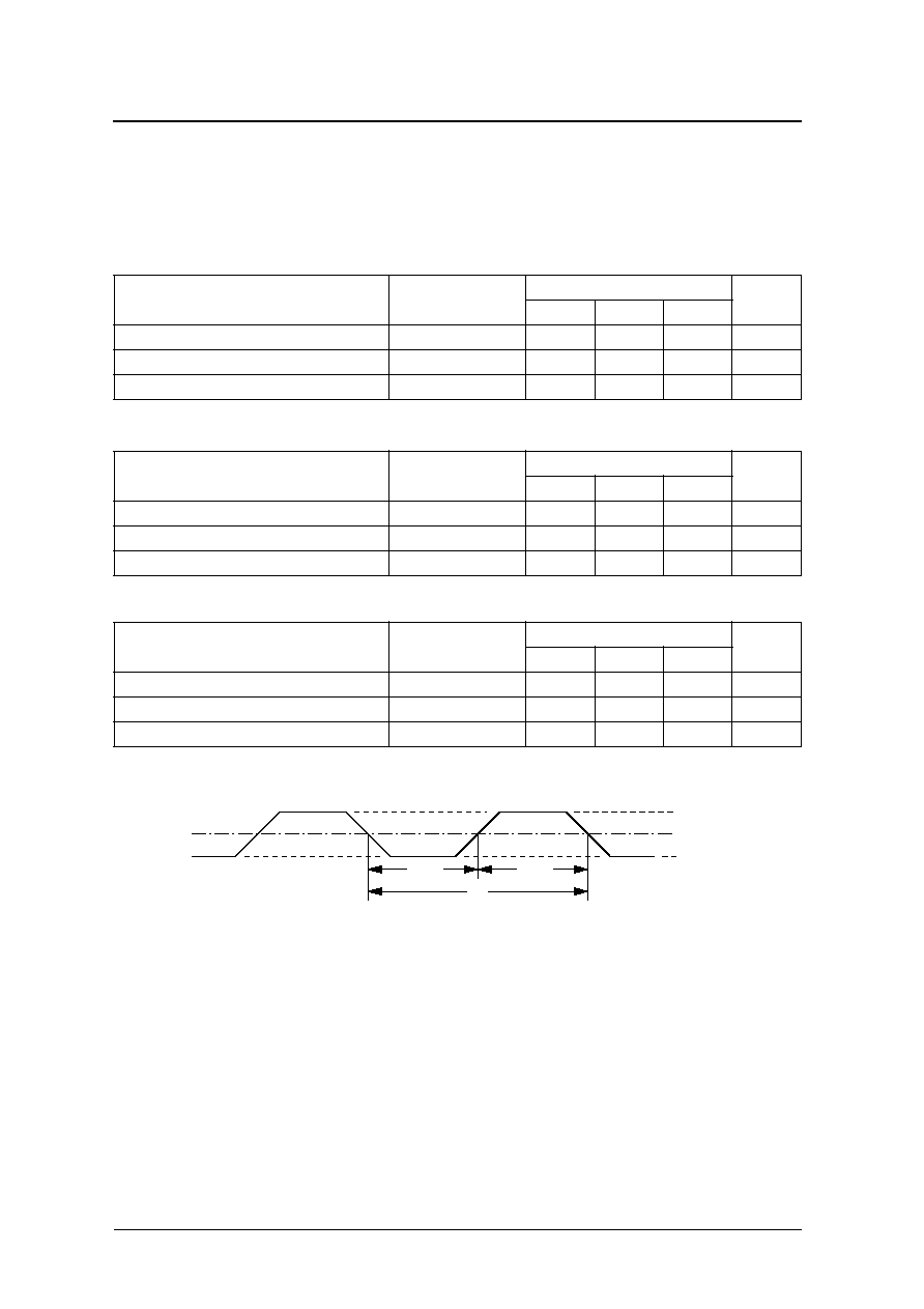
System clock (CLK)
256fs type
384fs type
512fs type
Parameter
Symbol
Rating
Unit
min
typ
max
HIGH-level clock pulsewidth
t
CWH
20.0
≠
125
ns
LOW-level clock pulsewidth
t
CWL
20.0
≠
125
ns
Clock pulse cycle
t
XI
40.0
≠
250
ns
Parameter
Symbol
Rating
Unit
min
typ
max
HIGH-level clock pulsewidth
t
CWH
13.15
≠
125
ns
LOW-level clock pulsewidth
t
CWL
13.15
≠
125
ns
Clock pulse cycle
t
XI
26.3
≠
250
ns
Parameter
Symbol
Rating
Unit
min
typ
max
HIGH-level clock pulsewidth
t
CWH
10
≠
125
ns
LOW-level clock pulsewidth
t
CWL
10
≠
125
ns
Clock pulse cycle
t
XI
20
≠
250
ns
V
IH1
V
IL1
0.5V
DD
XI
t
CLK
CWH
t
CWL
t
SM588
◊
series
NIPPON PRECISION CIRCUITS--6
Serial inputs
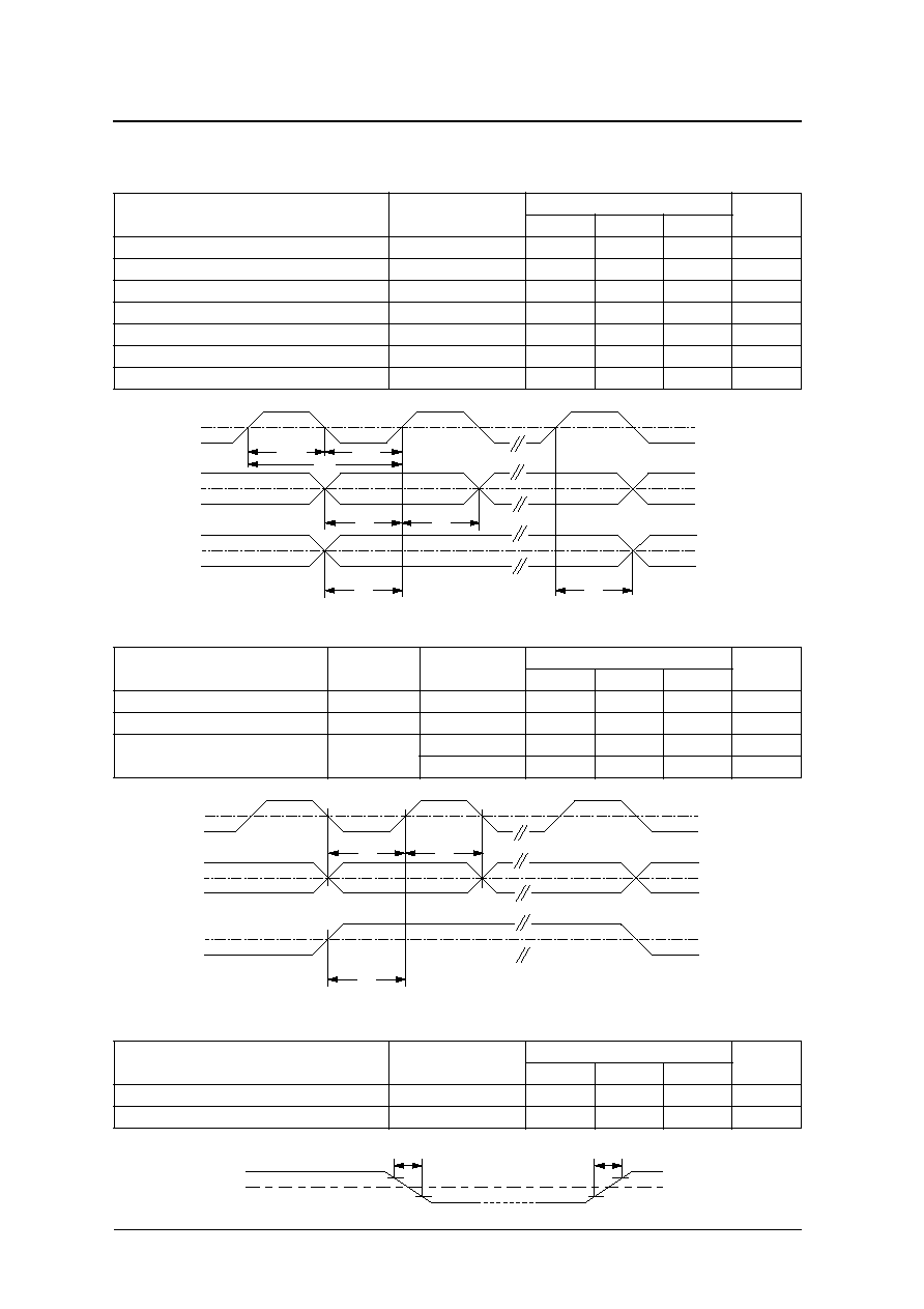
3-wire type (BCKI, DATA, LRCI)
2-wire type (DATA, LRCI)
Control input (DEEM: 2-wire type)
Parameter
Symbol
Rating
Unit
min
typ
max
BCKI HIGH-level pulsewidth
t
BCWH
50.0
≠
≠
ns
BCKI LOW-level pulsewidth
t
BCWL
50.0
≠
≠
ns
BCKI pulse cycle
t
BCY
1/(64fs)
≠
≠
ns
DATA setup time
t
DS
50.0
≠
≠
ns
DATA hold time
t
DH
50.0
≠
≠
ns
LRCI edge to first BCKI rising edge
t
LB
50.0
≠
≠
ns
Last BCKI rising edge to LRCI edge
t
BL
50.0
≠
≠
ns
Parameter
Symbol
Condition
Rating
Unit
min
typ
max
DATA setup time
t
DS
50
≠
≠
ns
DATA hold time
t
DH
50
≠
≠
ns
LRCI edge to internal BCLK rising edge
t
LB
256fs/512fs
1.5t
XI
≠
2.5t
XI
ns
384fs
3.5t
XI
≠
4.5t
XI
ns
Parameter
Symbol
Rating
Unit
min
typ
max
Rise time
t
r
≠
≠
50
ns
Fall time
t
f
≠
≠
50
ns
BCKI
DATA
LRCI
BCWH
t
BCWL
t
BCY
t
DS
t
DH
t
BL
t
LB
t
0.35V
DD
0.35V
DD
0.35V
DD
Internal
BCLK
DATA
LRCI
DS
t
DH
t
LB
t
0.35V
DD
0.35V
DD
0.35V
DD
DEEM
0.35V
DD
0.5V
DD
t
f
t
r
0.2V
DD
0.5V
DD
0.2V
DD
SM588
◊
series
NIPPON PRECISION CIRCUITS--7
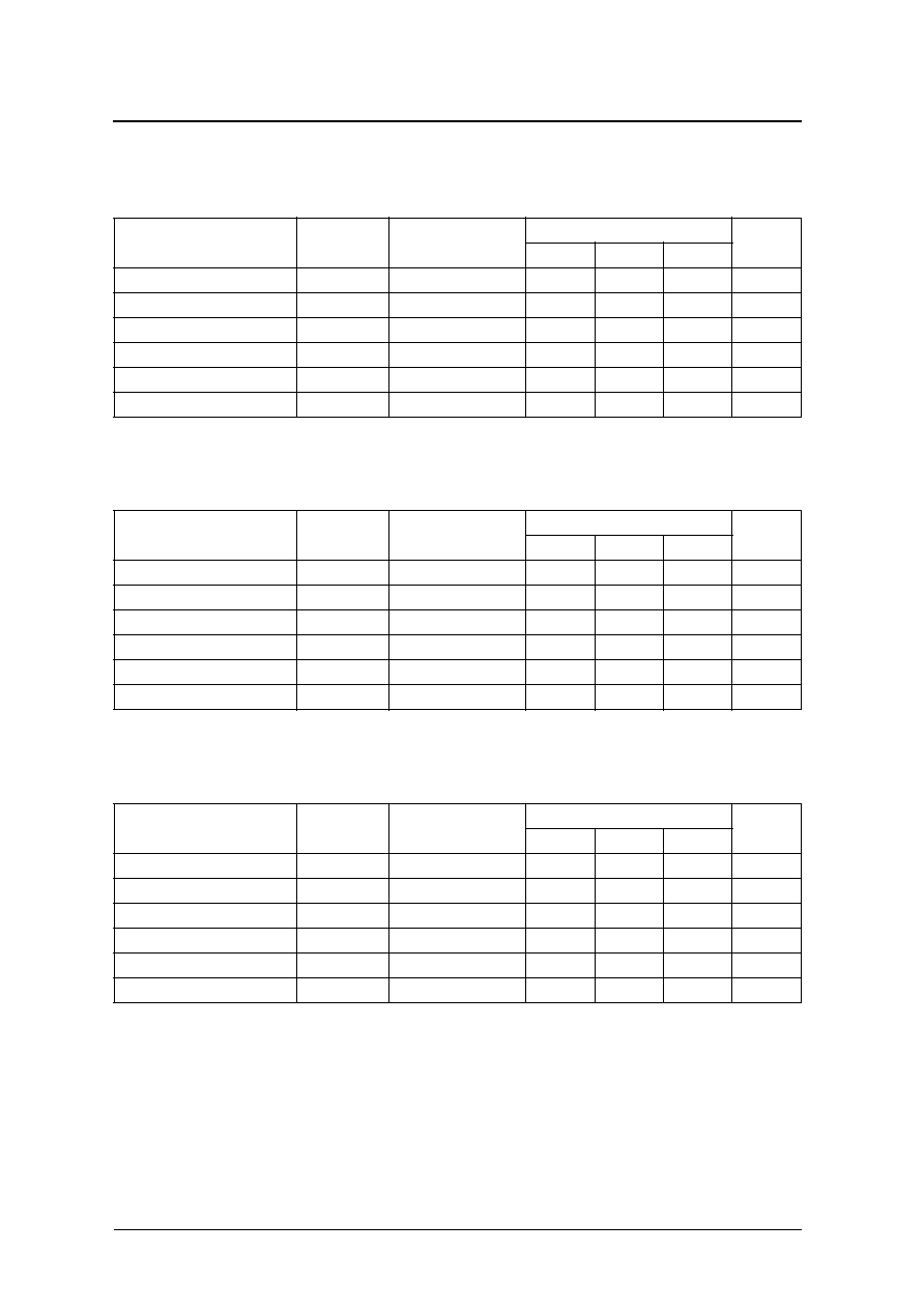
AC Analog Characteristics
256fs type specification (SM5883BS) : V
SS
= 0 V, V
DD
= 5 V, 16-bit input type,
crystal oscillator frequency f
OSC
= 11.2896 MHz, Ta = 25
∞C
Note: These parameters are measured using the measurement block diagram (page 8) and the measurement circuit (page 9).
384fs type specification (SM5882AS, SM5883AS) : V
SS
= 0 V, V
DD
= 5 V, DEEM = 0 V (2-wire type),
16-bit input type, crystal oscillator frequency f
OSC
= 16.9344 MHz, Ta = 25
∞C
Note: These parameters are measured using the measurement block diagram (page 8) and the measurement circuit (page 9).
512fs type specification (SM5885CS) : V
SS
= 0 V, V
DD
= 5 V, 24-bit input type,
crystal oscillator frequency f
OSC
= 22.5792MHz, Ta = 25
∞C
Note: These parameters are measured using the measurement block diagram (page 8) and the measurement circuit (page 9).
Parameter
Symbol
Condition
Rating
Unit
min
typ
max
Total harmonic distortion
THD
+ N
1 kHz, 0 dB
≠
0.0035
0.0130
%
LSI output level
V
OUT1
1 kHz, 0 dB
≠
1.09
≠
V
rms
Evaluation board output level
V
OUT2
1 kHz, 0 dB
≠
1.33
≠
V
rms
Dynamic range
D.R
1 kHz,
-60 dB
90.4
96.4
≠
dB
Signal-to-noise ratio
S/N
1 kHz, 0dB/
-
92.8
98.8
≠
dB
Channel separation
Ch. Sep
1 kHz,
- -0dB
87.5
93.5
≠
dB
Parameter
Symbol
Condition
Rating
Unit
min
typ
max
Total harmonic distortion
THD
+ N
1 kHz, 0 dB
≠
0.003
0.0120
%
LSI output level
V
OUT1
1 kHz, 0 dB
≠
1.09
≠
V
rms
Evaluation board output level
V
OUT2
1 kHz, 0 dB
≠
1.33
≠
V
rms
Dynamic range
D.R
1 kHz,
-60 dB
90.4
96.4
≠
dB
Signal-to-noise ratio
S/N
1 kHz, 0dB/
-
93.0
99.0
≠
dB
Channel separation
Ch. Sep
1 kHz,
- -0dB
88.5
94.5
≠
dB
Parameter
Symbol
Condition
Rating
Unit
min
typ
max
Total harmonic distortion
THD
+ N
1 kHz, 0 dB
≠
0.0035
0.0130
%
LSI output level
V
OUT1
1 kHz, 0 dB
≠
1.09
≠
V
rms
Evaluation board output level
V
OUT2
1 kHz, 0 dB
≠
1.33
≠
V
rms
Dynamic range
D.R
1 kHz,
-60 dB
92.0
98.0
≠
dB
Signal-to-noise ratio
S/N
1 kHz, 0dB/
-
92.8
98.8
≠
dB
Channel separation
Ch. Sep
1 kHz,
- -0dB
87.5
93.5
≠
dB

SM588
◊ series
NIPPON PRECISION CIRCUITS--8
AC analog measurement block diagram
AC analog measurement conditions
Parameter
1
1. Pins LO and RO should have an output load of 10 k
(min).
Symbol
3346A left/right-channel selector
switch
Audio Precision System Two audio
analyzer with built-in filter
Total harmonic distortion
THD
+ N
Not used
20 kHz lowpass filter
Output level
V
OUT
Dynamic range
D.R
D-RANGE
Signal-to-noise ratio
S/N
Not used
22 kHz lowpass filter
A-WTD
Channel separation
Ch. Sep
Not used
20 kHz lowpass filter
Evaluation
Board
NF Corporation
CD Player
EVA. Filter3346A
Left
Channel
Right
Channel
*Not available for 2-wire type
CLK
Audio Precision System Two
corresponds to SYS-2322
BCLK*
LRCK(fs)
fs= 44.1kHz
256fs/384fs
/512fs
Serial Interface Adaptor
corresponds to SIA-2322
100k
Input Impedance
DATA= 16/24bit
SM588
◊ series
NIPPON PRECISION CIRCUITS--9
AC analog measurement circuit
DATA
BCKI/DEEM
LRCI
CLK
33u
33u
+-
-+
27k
33k
33k
68p
2.2u
100p
22k
22k
100
100k
330p
33u
+
-
+
-
33u
0.1u
-
+
33u
33u
+-
-+
27k
33k
33k
68p
2.2u
100p
22k
22k
100
100k
330p
33u
+
-
-
+
L ch. OUT
R ch. OUT
-+
-+
-+
16.9344MHz(384fs)
11.2896MHz(256fs)
22.5792MHz(512fs)
0.01u
+
-
470u
8
2
3
6
8
5
100u
VDD
VSS
VCC
VEE
NJM
2100
0.01u
DATA
RO
VSS
VDD
LO
CLK
BCKI /DEEM
LRCI
8
X'tal
1M
74HCU04
1
2
5
6
7
10
9
12
11
14
13
4
3
0.01u
NJM
2100
SM5882/83/85
10p
10p
2
5
6
3
1
4
Int. CLK
Ext. CLK
1
7
SM588
◊ series
NIPPON PRECISION CIRCUITS--10
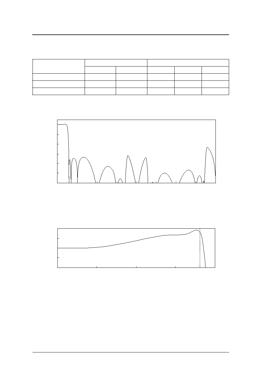
Theoretical Filter Characteristics
Overall characteristics
Overall frequency characteristic
Passband characteristic
Parameter
Frequency band
Attenuation (dB)
f
@ fs = 44.1 kHz
min
typ
max
Passband ripple
0 to 0.4535fs
0 to 20.0 kHz
-0.05
≠
+0.05
Stopband attenuation
0.5465fs to 7.4535fs
24.1 to 328.7 kHz
32
≠
≠
Built-in analog LPF compensation
0.4535fs
20.0 kHz
≠
-0.34
≠
Gain(dB)
0.0
1.0
2.0
3.0
4.0
5.0
6.0
7.0
8.0
60
50
40
30
20
10
0
(
◊ fs)
0.000
0.125
0.250
0.375
0.500
0.8
0.6
0.4
0.2
0.0
0.4535
(
◊
fs)
Gain(dB)
SM588
◊ series
NIPPON PRECISION CIRCUITS--11
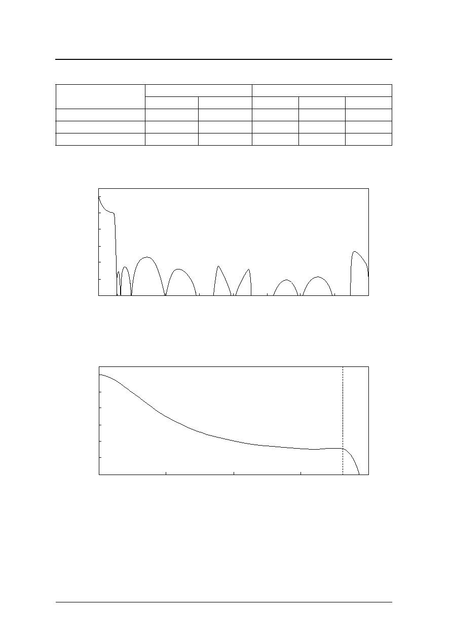
2-wire input, deemphasis ON overall characteristics
Deemphasis ON overall frequency characteristic
Deemphasis ON passband characteristic
Parameter
Frequency band
Attenuation (dB)
f
@ fs = 44.1 kHz
min
typ
max
Passband ripple
0 to 0.4535fs
0 to 20.0 kHz
-0.09
≠
+0.23
Stopband attenuation
0.5465fs to 7.4535fs
24.1 to 328.7 kHz
36
≠
≠
Built-in analog LPF compensation
0.4535fs
20.0 kHz
≠
-0.34
≠
Gain(dB)
(
◊
fs)
0.0
1.0
2.0
3.0
4.0
5.0
6.0
7.0
8.0
0
10
20
30
40
50
60
(
◊
fs)
Gain(dB)
0.000
0.125
0.250
0.375
0.500
12
10
8
6
4
2
0
0.4535
SM588
◊ series
NIPPON PRECISION CIRCUITS--12
FUNCTIONAL DESCRIPTION
System Clock (CLK)
The system clock CLK frequency varies with device within the series as shown below, where fs is the input
frequency on LRCI.
Note that the input clock accuracy and signal-to-noise ratio greatly influence the AC analog characteristics.
The D/A converter operates at the speed shown in the following table.
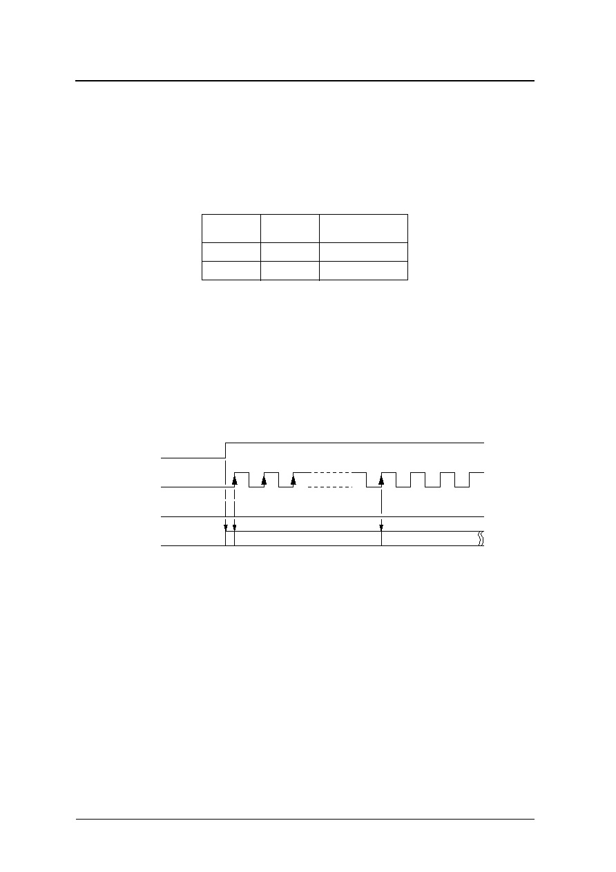
System Reset
The SM588
◊ series devices incorporate a built-in power-ON reset circuit for system reset.
When power is applied, the internal arithmetic operation and output timing counter are reset, and then reset
again and timing synchronized to the external input on the next LRCI rising edge. After system reset, the out-
puts are muted until the 9th rising of LRCI when output muting is released.
When the timing is reset, the PWM outputs may generate an output noise. An external muting circuit may be
required to prevent this output noise.
Table 1. System clock
Device
Master clock
DAC oversampling
operation
A version
384fs
48fs
B, C version
256/512fs
32fs
Figure 1. System reset timing
LRCI
VDD
Internal
Reset
LO
RO
Output Muted
1
2
3
9
10
SM588
◊ series
NIPPON PRECISION CIRCUITS--13
Audio Data Input
Input data format (DATA)
The input data has a format that varies with device within the series, as shown below.
Input timing
3-wire input (DATA, LRCI, BCKI)
Serial data bits on DATA are read into the SIPO register (serial-to-parallel converter register) on the rising
edge of the bit clock BCKI, and then converted to parallel data.
The arithmetic operation and output timing are independent of the input timing. Accordingly, after a reset, as
long as the clock frequency ratio between LRCI and the system clock CLK is maintained, phase differences
between LRCI, BCKI and the system clock CLK do not affect the functional operation. Also, any jitter present
on the data input clock does not appear as output pulse jitter.
2-wire input (DATA, LRCI)
Serial data bits on DATA are read into the SIPO register (serial-to-parallel converter register) on the rising
edge of an internally generated bit clock, and then converted to parallel data.
Deemphasis Filter (DEEM: 2-wire input)
The 2-wire type with built-in digital deemphasis filter is designed to operate at 44.1 kHz. Deemphasis is ON
when DEEM is HIGH, and OFF when DEEM is LOW.
Table 2. Input format
Device
Input length
Format
SM5882/SM5883
1
1. The 2-wire type supports bit clocks of 48fs (384fs) or 64fs (256fs/512fs) only.
16 bits
MSB first, bit serial, rear-packed,
2s complement
SM5885
2
2. The 3-wire type supports bit clocks of up to 64fs.
24 bits
SM588
◊ series
NIPPON PRECISION CIRCUITS--14
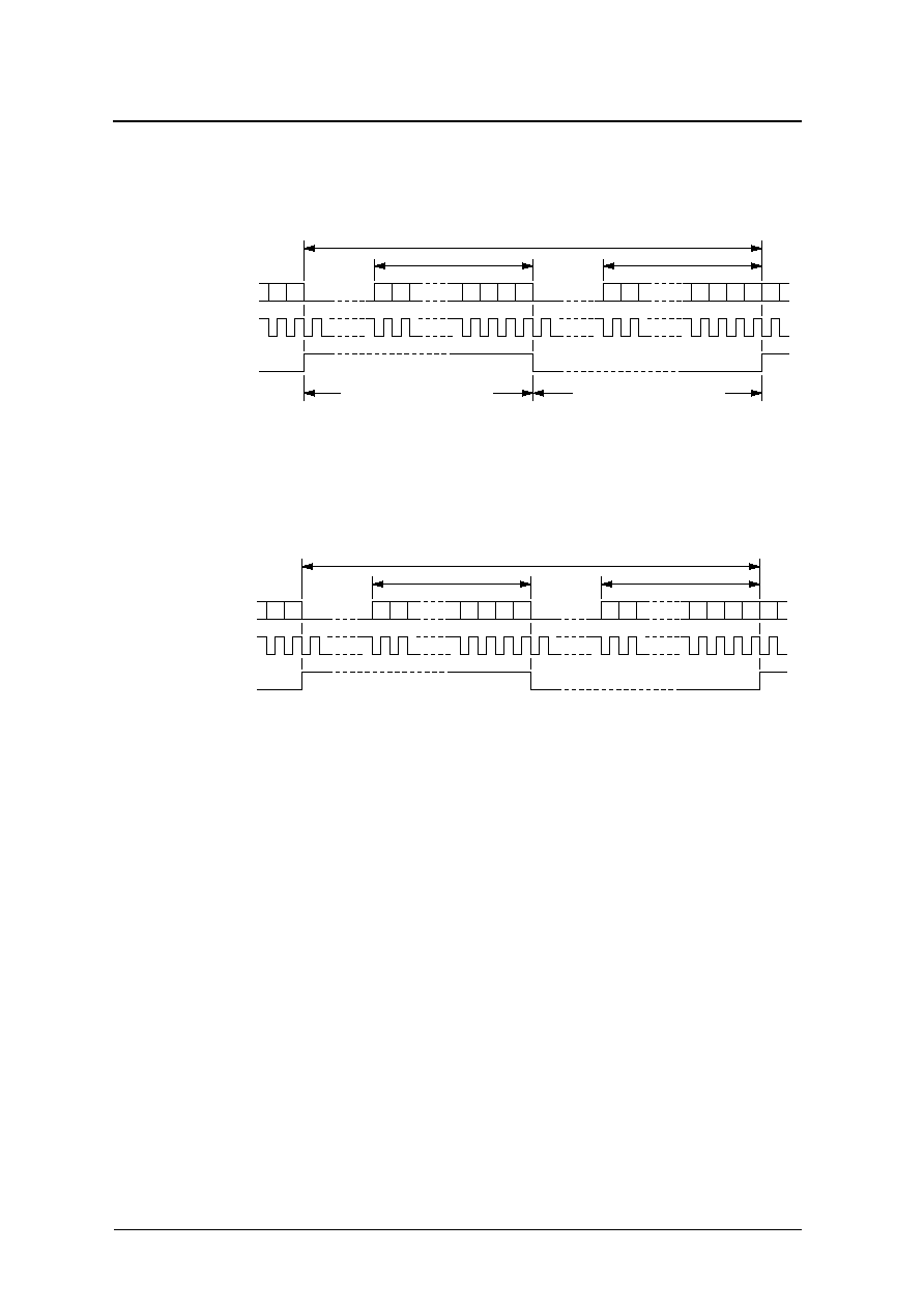
TIMING DIAGRAMS
2-wire Input Type with Deemphasis Filter Built-in
3-wire Input Type
1/fs
Left
Channel
Right
Channel
LSB
16 or 24 bit
MSB
LSB
16 or 24 bit
MSB
DATA
LRCI
Internal bit clock
(Generated by system clock)
24 bit clock (384fs type)
32 bit clock (256fs/512fs type)
24 bit clock (384fs type)
32 bit clock (256fs/512fs type)
1/fs
Left
Channel
Right
Channel
LSB
16 or 24 bit
MSB
LSB
16 or 24 bit
MSB
DATA
BCKI
(64fs MAX)
LRCI
SM588
◊ series
NIPPON PRECISION CIRCUITS--15
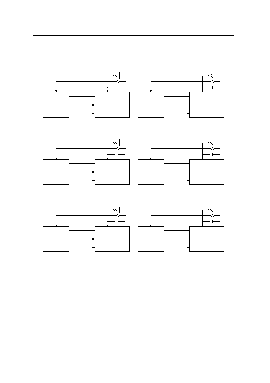
TYPICAL APPLICATIONS
Input Interface Examples
(fs = 44.1kHz)
Note that the output analog characteristics and other specifications are not guaranteed for a particular format or application circuit.
SM5882/83/85
44.1kHz
CKI
LRCI
DATA
X'tal
16.9344MHz (384fs)
SM5882/83/85
44.1kHz
CKI
LRCI
DATA
BCKI
X'tal
16.9344MHz (384fs)
3-wire input type
System clock 384fs
2-wire input type
System clock 384fs
SM5882/83/85
44.1kHz
CKI
LRCI
DATA
BCKI
X'tal
11.2896MHz (256fs)
3-wire input type
System clock 256fs
SM5882/83/85
44.1kHz
CKI
LRCI
DATA
X'tal
11.2896MHz (256fs)
2-wire input type
System clock 256fs
SM5882/83/85
44.1kHz
CKI
LRCI
DATA
BCKI
X'tal
22.5792MHz (512fs)
3-wire input type
System clock 512fs
SM5882/83/85
44.1kHz
CKI
LRCI
DATA
X'tal
22.5792MHz (512fs)
2-wire input type
System clock 512fs

SM588
◊ series
NIPPON PRECISION CIRCUITS--16
NC9720GE
2000.11
NIPPON PRECISION CIRCUITS INC. reserves the right to make changes to the products described in this data sheet in order to
improve the design or performance and to supply the best possible products. Nippon Precision Circuits Inc. assumes no responsibility for
the use of any circuits shown in this data sheet, conveys no license under any patent or other rights, and makes no claim that the circuits
are free from patent infringement. Applications for any devices shown in this data sheet are for illustration only and Nippon Precision
Circuits Inc. makes no claim or warranty that such applications will be suitable for the use specified without further testing or modification.
The products described in this data sheet are not intended to use for the apparatus which influence human lives due to the failure or
malfunction of the products. Customers are requested to comply with applicable laws and regulations in effect now and hereinafter,
including compliance with export controls on the distribution or dissemination of the products. Customers shall not export, directly or
indirectly, any products without first obtaining required licenses and approvals from appropriate government agencies.
NIPPON PRECISION CIRCUITS INC.
4-3, Fukuzumi 2-chome
Koto-ku, Tokyo 135-8430, Japan
Telephone: +81-3-3642-6661
Facsimile: +81-3-3642-6698
http://www.npc.co.jp/
Email: sales
@
npc.co.jp
NIPPON PRECISION CIRCUITS INC.