 | –≠–ª–µ–∫—Ç—Ä–æ–Ω–Ω—ã–π –∫–æ–º–ø–æ–Ω–µ–Ω—Ç: SM5904BF | –°–∫–∞—á–∞—Ç—å:  PDF PDF  ZIP ZIP |

NIPPON PRECISION CIRCUITS INC.
NIPPON PRECISION CIRCUITS-1
SM5904BF
compression and non compression type
shock-proof memory controller
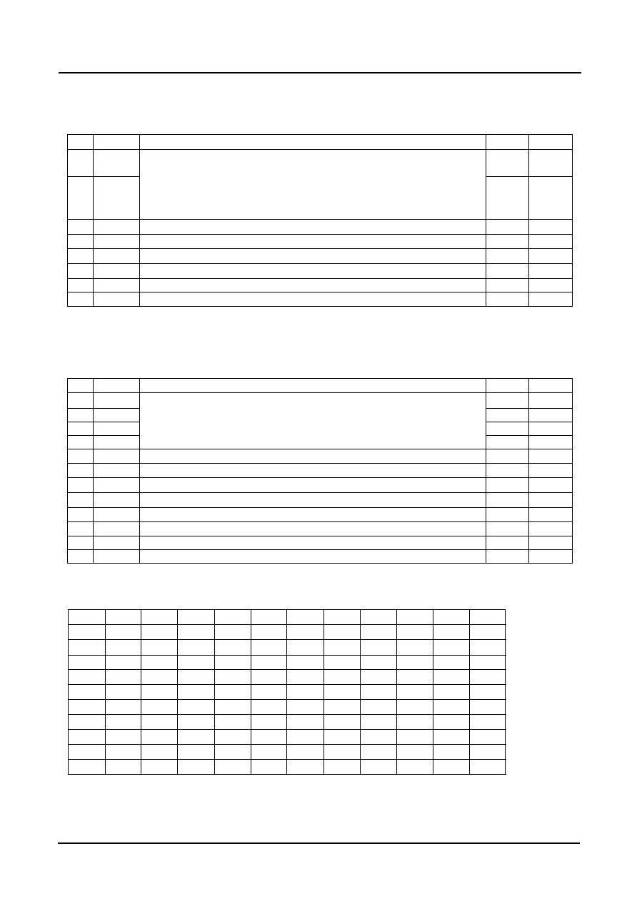
Overview
- 2-channel processing
- Serial data input
2s complement, 16-bit/MSB first, right-justified
format
- Wide capture function
(up to 3
◊
speed input rate)
- System clock input
384fs (16.9344 MHz)
- Shock-proof memory controller
ADPCM compression method
4-level compression mode selectable
4-bit compression mode 2.78 s/Mbit
5-bit compression mode 2.22 s/Mbit
6-bit compression mode 1.85 s/Mbit
Full-bit non compression mode 0.74 s/Mbit
External DRAM configurations usable
2
◊
4M DRAM (1M
◊
4 bits)
Internal and External 4M DRAM
1
◊
4M DRAM (1M
◊
4 bits)
Only Internal 4M DRAM
- Compression mode selectable
- Microcontroller interface
Serial command write and status read-out
Data residual detector:
15-bit operation, 16-bit output
Digital attenuator
8-bit setting
Soft attenuator function
Noiseless attenuation-level switching
(256- step switching in 23 ms max.)
Soft mute function
Mute ON in 23 ms max.
Direct return after soft mute release
Forced mute
- Extension I/O
Microcontroller interface for external control
using 4 extension I/O pins
- +2.4 to + 3.3 V operating voltage range
- Schmitt inputs
All input pins (including I/O pins) except CLK
(system clock)
- Reset signal noise elimination
Approximately 3.8
µ
s or longer (65 system
clock pulses) continuous LOW-level reset
- Digital audio interface (DIT)
- 44-pin QFP package (0.8 mm pin pitch)
The SM5904BF is a compression and non com-
pression type shock-proof memory controller LSI for
compact disc players. The compression level can
be set in 4 levels, and external 4M DRAM can be
connected to expand the memory to 4M bits. Digital
attenuator, soft mute and related functions are also
incorporated. It operates from a 2.4 to 3.3 V supply
voltage range.
Features
Ordering Information
SM5904BF
44pin QFP
NIPPON PRECISION CIRCUITS-2
SM5904BF
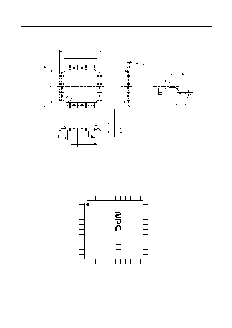
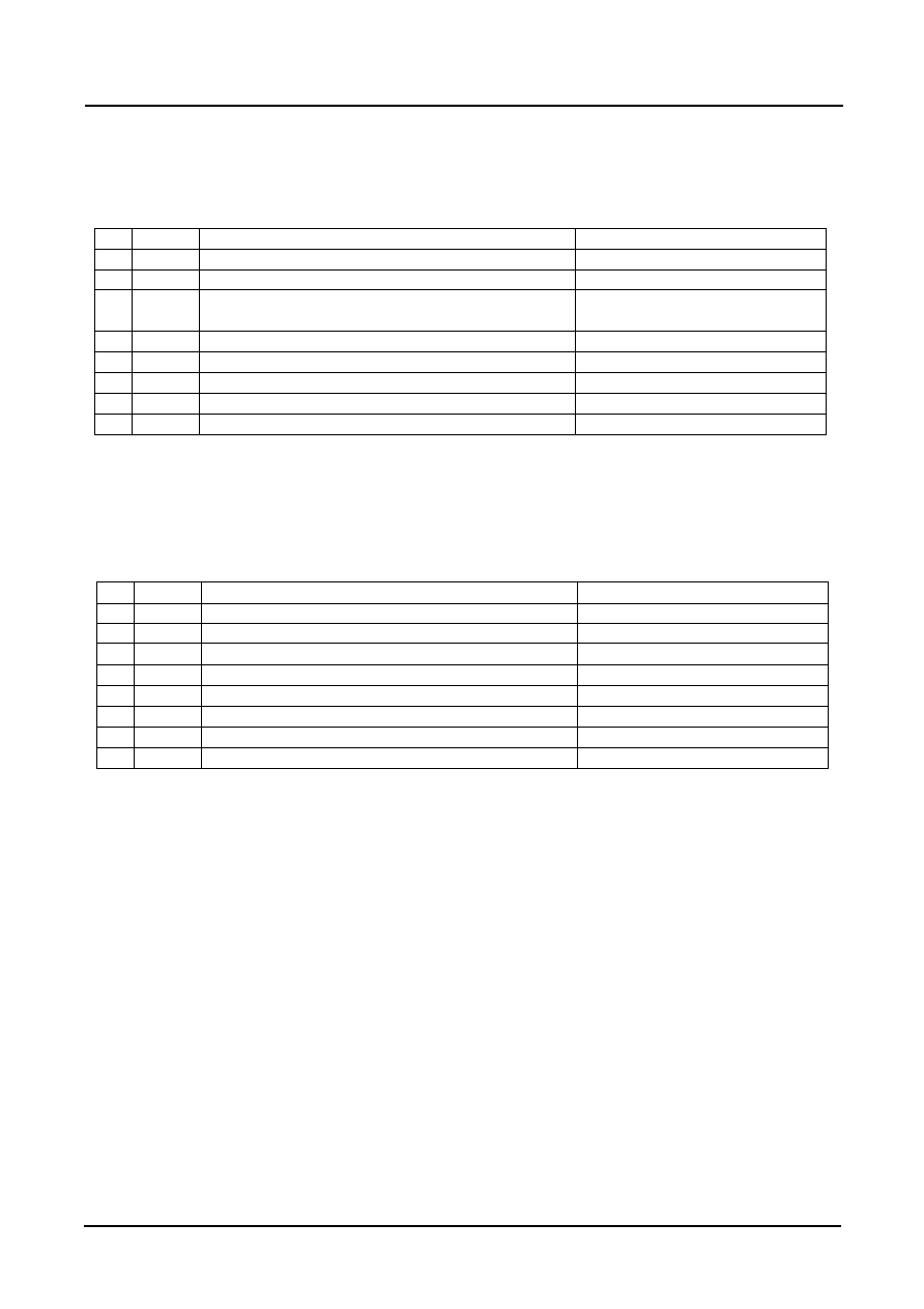
Package dimensions
(Unit: mm)
44-pin QFP
13.20 0.30
10.00 0.20
13.20 0.30
+
10.00 0.20
+
0.10MAX
0.35+
0.05
0.10
2.30MAX
2.05 0.10
+
0.15 0.10
+
0.15MAX
0.15+
0.05
0.10
0 to 8
0.80 0.20
1.60
0.80
+
+
+
Pinout
(Top View)
1
2
3
4
5
6
7
8
9
10
11
12
13
14
15
16
17
18
19
20
21
22
23
24
25
26
27
28
29
30
31
32
33
34
35
36
37
38
39
40
41
42
43
44
VDD2
UC1
UC2
UC3
UC4
VSS2
DIT
NTEST1
CLK
VSS1
YSRDATA
NWE
D1
D0
D3
D2
NCAS2
NTEST2
YMCLK
YMDATA
YMLD
YDMUTE
YLRCK
YSCK
ZSCK
ZLRCK
ZSRDATA
YFLAG
YFCLK
YBLKCK
NRESET
ZSENSE
VDD1
A3
A2
A1
A0
A4
A5
A6
A7
A8
A9
NRAS
S
M
590
4B
F
NIPPON PRECISION CIRCUITS-3
SM5904BF
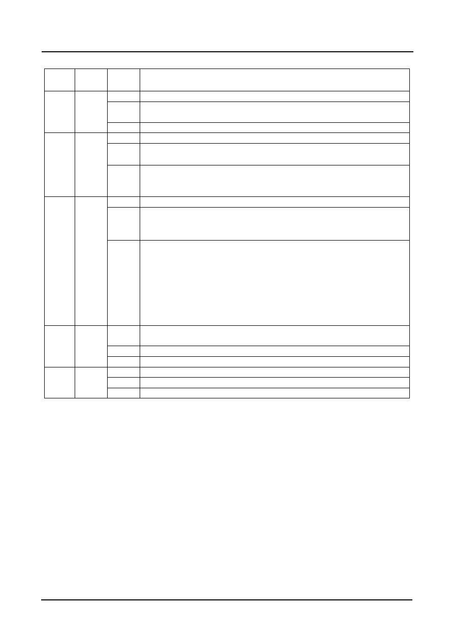
Pin number
Pin name
I/O
Function
Setting
H
L
1
VDD2
-
VDD supply pin
2
UC1
Ip/O
Microcontroller interface extension I/O 1
3
UC2
Ip/O
Microcontroller interface extension I/O 2
4
UC3
Ip/O
Microcontroller interface extension I/O 3
5
UC4
Ip/O
Microcontroller interface extension I/O 4
6
VSS2
-
Ground
7
DIT
O
Digital audio interface
8
NTEST1
Ip
Test pin
Test
9
CLK
I
16.9344 MHz clock input
10
VSS1
-
Ground
11
YSRDATA
I
Audio serial input data
12
YLRCK
I
Audio serial input LR clock
Left channel
Right channel
13
YSCK
I
Audio serial input bit clock
14
ZSCK
O
Audio serial output bit clock
15
ZLRCK
O
Audio serial output LR clock
Left channel
Right channel
16
ZSRDATA
O
Audio serial output data
17
YFLAG
I
Signal processor IC RAM overflow flag
Overflow
18
YFCLK
I
Crystal-controlled frame clock
19
YBLKCK
I
Subcode block clock signal
20
NRESET
I
System reset pin
Reset
21
ZSENSE
O
Microcontroller interface status output
22
VDD1
-
VDD supply pin
23
YDMUTE
I
Forced mute pin
Mute
24
YMLD
I
Microcontroller interface latch clock
25
YMDATA
I
Microcontroller interface serial data
26
YMCLK
I
Microcontroller interface shift clock
27
NTEST2
Ip
Test pin
Test
28
NCAS2
O
DRAM2 CAS control(Use External DRAM)
29
D2
Ip/O
DRAM data input/output 2
30
D3
Ip/O
DRAM data input/output 3
31
D0
Ip/O
DRAM data input/output 0
32
D1
Ip/O
DRAM data input/output 1
33
NWE
O
DRAM WE control
34
NRAS
O
DRAM RAS control
35
A9
O
DRAM address 9
36
A8
O
DRAM address 8
37
A7
O
DRAM address 7
38
A6
O
DRAM address 6
39
A5
O
DRAM address 5
40
A4
O
DRAM address 4
41
A0
O
DRAM address 0
42
A1
O
DRAM address 1
43
A2
O
DRAM address 2
44
A3
O
DRAM address 3
Ip : Input pin with pull-up resistor Ip/O : Input/Output pin (With pull-up resistor when in input mode)
28, 33 to 44 pins for high-impedance output and 29 to 32 pins for input pull-up condition except for using external DRAM.
Pin description
NIPPON PRECISION CIRCUITS-4
SM5904BF
Parameter
Symbol
Rating
Unit
Supply voltage
V
DD
- 0.3 to 4.6
V
Input voltage
V
I
V
SS
- 0.3 to V
DD
+ 0.3
V
Storage temperature
T
STG
- 40 to 125
∞C
Power dissipation
P
D
600
mW
Soldering temperature
T
SLD
255
∞C
Soldering time
t
SLD
10
sec
(V
SS
= 0V, VDD1, VDD2 pin voltage = V
DD
)
(*1) Refer to pin summary on the next page.
Note. Values also apply for supply inrush and switch-off.
Parameter
Symbol
Rating
Unit
Supply voltage
V
DD
2.4 to 3.3
V
Operating temperature
T
OPR
-
10 to 70
∞C
(V
SS
= 0V, VDD1, VDD2 pin voltage = V
DD
)
Parameter
Pin
Symbol
Condition
Rating
Unit
Min
Typ
Max
Current consumption
VDD
I
DD
(*A)SHPRF ON
9
18
mA
(*A)Through mode
2.6
5
mA
Input voltage
CLK
H level
V
IH1
0.7V
DD
V
L level
V
IL1
0.3V
DD
V
V
INAC
AC coupling
1.0
V
P-P
(*2,3,4)
H level
V
IH2
0.8V
DD
V
L level
V
IL2
0.2V
DD
V
(*5)
H level
V
IH3
0.8V
DD
V
L level
V
IL3
0.2V
DD
V
Output voltage
(*4,6)
H level
V
OH1
I
OH
= - 0.5 mA
V
DD
- 0.4
V
L level
V
OL1
I
OL
= 0.5 mA
0.4
V
(*5,7)
H level
V
OH2
I
OH
= - 0.5 mA
V
DD
- 0.4
V
L level
V
OL2
I
OL
= 0.5 mA
0.4
V
Input current
CLK
I
IH1
V
IN
= V
DD
10
30
60
µ
A
I
IL1
V
IN
= 0V
10
30
60
µ
A
(*3)
I
IL2
V
IN
= 0V
6
25
200
µ
A
(*4,5)
I
IL3
V
IN
= 0V
1
3
6
µ
A
Input leakage current
(*2,3,4,5)
I
LH
V
IN
= V
DD
- 10
10
µ
A
(*2)
I
LL
V
IN
= 0V
- 10
10
µ
A
(*A) V
DD1
= V
DD2
= 3 V, CLK input frequency f
XTI
= 384fs = 16.9344 MHz, all outputs unloaded,
SHPRF: Shock-proof,
typical values are for V
DD1
= V
DD2
= 3 V.
Electrical characteristics
Recommended operating conditions
DC characteristics
Standard voltage: (V
DD1
= V
DD2
= 2.4 to 3.3 V, V
SS
= 0 V, Ta =
-
10 to 70 ∞C)
Absolute maximum ratings
NIPPON PRECISION CIRCUITS-5
SM5904BF
(*1)
Pin function
Clock input pin (AC input)
Pin name
CLK
(*2)
Pin function
Schmitt input pins
Pin name
YSRDATA, YLRCK, YSCK, YFLAG, YFCLK, NRESET,
YBLKCK, YDMUTE, YMLD, YMDATA, YMCLK
(*3)
Pin function
Schmitt input pin with pull-up
Pin name
NTEST1, NTEST2
(*4)
Pin function
I/O pins (Schmitt input with pull-up in input state)
Pin name
UC1, UC2, UC3, UC4
(*5)
Pin function
I/O pins (Schmitt input with pull-up in input state)
Pin name
D0, D1, D2, D3
(*6)
Pin function
Outputs
Pin name
ZSCK, ZLRCK, ZSRDATA, ZSENSE
(*7)
Pin function
Outputs
Pin name
NCAS2, NWE, NRAS, A0, A1, A2, A3, A4, A5, A6, A7, A8, A9, DIT
<Pin summary>
NIPPON PRECISION CIRCUITS-6
SM5904BF
Parameter
Symbol
Condition
Rating
Unit
System clock
Min
Typ
Max
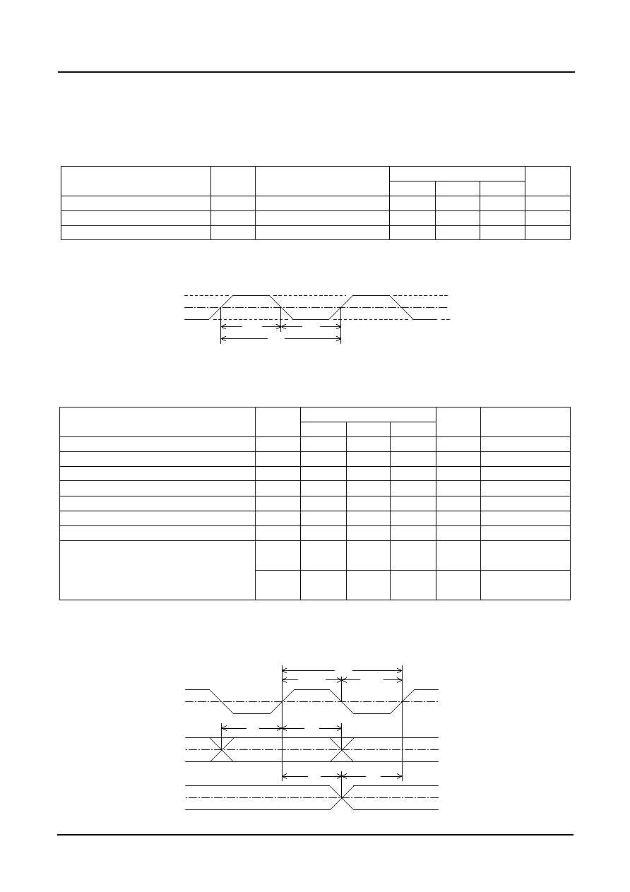
Clock pulsewidth (HIGH level)
t
CWH
26
29.5
125
ns
Clock pulsewidth (LOW level)
t
CWL
26
29.5
125
ns
Clock pulse cycle
t
CY
384fs
56
59
250
ns
CWH
t
CWL
t
CY
t
0.5V
DD
CLK
Parameter
Symbol
Rating
Unit
Condition
Min
Typ
Max
YSCK pulsewidth (HIGH level)
t
BCWH
75
ns
YSCK pulsewidth (LOW level)
t
BCWL
75
ns
YSCK pulse cycle
t
BCY
150
ns
YSRDATA setup time
t
DS
50
ns
YSRDATA hold time
t
DH
50
ns
Last YSCK rising edge to YLRCK edge
t
BL
50
ns
YLRCK edge to first YSCK rising edge
t
LB
50
ns
0
3fs
Memory system ON
YLRCK pulse frequency
(MSON=H)
See note below.
fs
fs
Memory system OFF
(MSON=L)
Note. When the memory system is OFF (through mode), the input data rate is synchronized to the system clock input (384fs), so input
data needs to be at 1/384 of this frequency. But, this IC can tolerate a certain amount of jitter. For details, refer to Through-mode
operation.
YSCK
YSRDATA
YLRCK
BCY
t
DS
t
DH
t
BCWH
t
BCWL
t
LB
t
BL
t
0.5V
DD
0.5V
DD
0.5V
DD
Serial input (YSRDATA, YLRCK, YSCK pins)
AC characteristics
Standard voltage: V
DD1
= V
DD2
= 2.4 to 3.3 V, V
SS
= 0 V, Ta =
-
10 to 70 ∞C
(*) Typical values are for fs = 44.1 kHz
System clock (CLK pin)
System clock input
NIPPON PRECISION CIRCUITS-7
SM5904BF
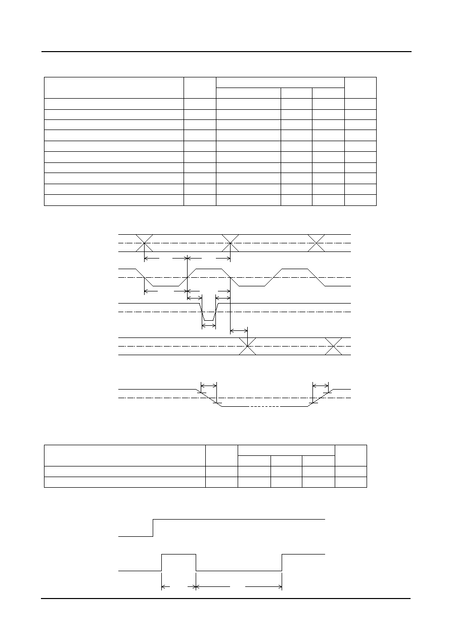
Parameter
Symbol
Rating
Unit
Min
Typ
Max
YMCLK LOW-level pulsewidth
t
MCWL
30 + 2
t
CY
ns
YMCLK HIGH-level pulsewidth
t
MCWH
30 + 2
t
CY
ns
YMDATA setup time
t
MDS
30 +
t
CY
ns
YMDATA hold time
t
MDH
30 +
t
CY
ns
YMLD LOW-level pulsewidth
t
MLWL
30 + 2
t
CY
ns
YMLD setup time
t
MLS
30 +
t
CY
ns
YMLD hold time
t
MLH
30 +
t
CY
ns
Rise time
t
r
100
ns
Fall time
t
f
100
ns
ZSENSE output delay
t
PZS
100 + 3
t
CY
ns
Note.
t
CY
is the system clock cycle time (59ns typ).
YMDATA
YMCLK
ZSENSE
YMLD
YMDATA
YMCLK
YMLD
MDS
t
MDH
t
MCWL
t
MLS
t
MCWH
t
MLH
t
MLWL
t
PZS
t
0.5V
DD
0.5V
DD
0.5V
DD
0.5V
DD
0.5V
DD
0.5V
DD
0.3 V
DD
0.3 V
DD
0.7 V
DD
0.7 V
DD
f
t
r
t
Reset input (NRESET pin)
Parameter
Symbol
Rating
Unit
Min
Typ
Max
First HIGH-level after supply voltage rising edge
t
HNRST
0
t
CY
(Note)
NRESET pulsewidth
t
NRST
64
t
CY
(Note)
Note.
t
CY
is the system clock (CLK) input (384fs) cycle time.
t
CY
= 59 ns,
t
NRST
(min) = 3.8
µ
s when fs = 44.1 kHz
NRESET
VDD1,VDD2
HNRST
t
t
NRST
Microcontroller interface (YMCLK, YMDATA, YMLD, ZSENSE pins)
NIPPON PRECISION CIRCUITS-8
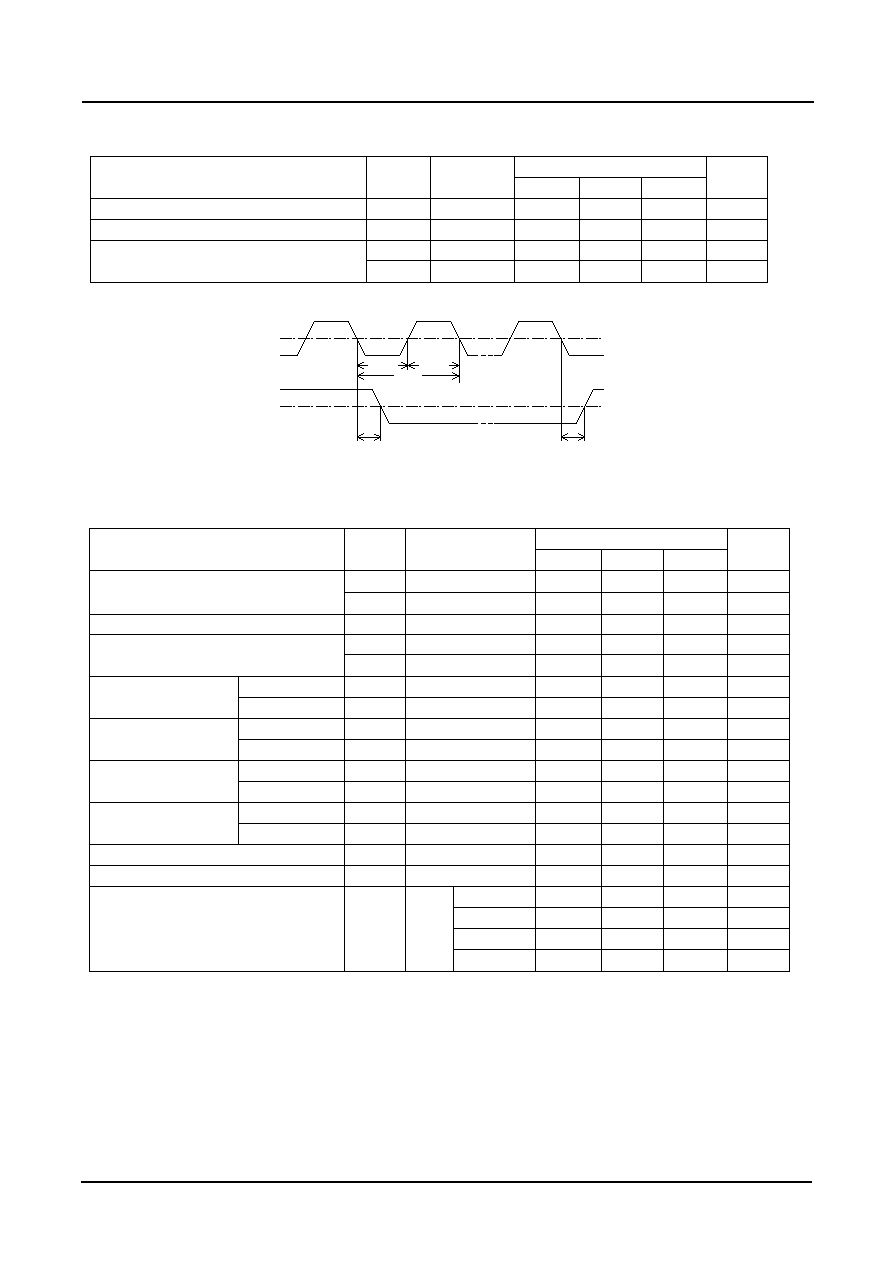
SM5904BF
Parameter
Symbol
Condition
Rating
Unit
Min
Typ
Max
ZSCK pulsewidth
t
SCOW
15 pF load
1/96fs
ZSCK pulse cycle
t
SCOY
15 pF load
1/48fs
ZSRDATA and ZLRCK output delay time
t
DHL
15 pF load
0
60
ns
t
DLH
15 pF load
0
60
ns
DRAM access timing (NRAS, NCAS2, NWE, A0 to A9, D0 to D3)
Parameter
Symbol
Condition
Rating
Unit
Min
Typ
Max
NRAS pulsewidth
t
RASL
15 pF load
5
t
CY
(note)
t
RASH
15 pF load
3
t
CY
NRAS falling edge to NCAS2 falling edge
t
RCD
15 pF load
2
t
CY
NCAS2 pulsewidth
t
CASH
15 pF load
5
t
CY
t
CASL
15 pF load
3
t
CY
NRAS
Setup time
t
RADS
15 pF load
1
t
CY
falling edge to address
Hold time
t
RADH
15 pF load
1
t
CY
NCAS2
Setup time
t
CADS
15 pF load
1
t
CY
falling edge to address
Hold time
t
CADH
15 pF load
5
t
CY
NCAS2
Setup time
t
CWDS
15 pF load
3
t
CY
falling edge to data write
Hold time
t
CWDH
15 pF load
3
t
CY
NCAS2
Input setup
t
CRDS
40
ns
rising edge to data read
Input hold
t
CRDH
0
ns
NWE pulsewidth
t
WEL
15 pF load
6
t
CY
NWE falling edge to NCAS2 falling edge
t
WCS
15 pF load
3
t
CY
Refresh cycle
Non
compression
2.8
ms
(fs = 44.1 kHz playback)
t
REF
4M
6-bit compression
7.3
ms
Memory system ON
DRAM
5-bit compression
8.8
ms
Decode sequence operation(READ=H)
◊ 1
or
◊ 2
4-bit compression
10.9
ms
Note.
t
CY
is the system clock (CLK) input (384fs) cycle time.
t
CY
= 59 ns when fs = 44.1 kHz
ZSCK
ZSRDATA
0.5V
DD
DLH
ZLRCK
0.5V
DD
DHL
t
t
DLH
SCOW
t
t
SCOW
t
SCOY
t
Serial output (ZSRDATA, ZLRCK, ZSCK pins)
NIPPON PRECISION CIRCUITS-9
SM5904BF
,,,,,,,,,
,,,,,,,,,
,,,,,,,,,
,,,,,,,,,
,,,,,,,,,,,,,,,,,,,,,,,,,
,,,,,,,,,,,,,,,,,,,,,,,,,
,,,,,,,,,,,,,,,,,,,,,,,,,
,,,,,,,,,,,,,,,,,,,,,,,,,
,,,,,,,,,,,,,,,,,,,,,,,,,
,,,,,,,,,,,,,,
,,,,,,,,,,,,,,
,,,,,,,,,,,,,,
,,,,,,,,,,,,,,
,,,,,,,,,,,,,,,,,,,,,,,,,,,,,,,,,
,,,,,,,,,,,,,,,,,,,,,,,,,,,,,,,,,
,,,,,,,,,,,,,,,,,,,,,,,,,,,,,,,,,
,,,,,,,,,,,,,,,,,,,,,,,,,,,,,,,,,
,,,,,,,,,,,,,,,,,,,,,,,,,,,,,,,,,
,,,,,,,,,,,,
,,,,,,,,,,,,
,,,,,,,,,,,,
,,,,,,,,,,,,
,,,,,,,
,,,,,,,
,,,,,,,
,,,,,,,
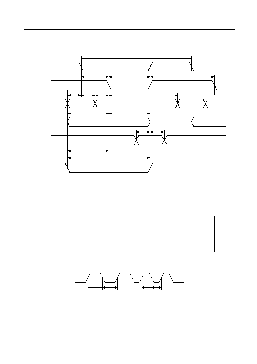
NCAS2
A0 to A9
D0 to D3
(WRITE)
NRAS
D0 to D3
(READ)
NWE
(WRITE)
3
WCS
t
6
WEL
t
CRDH
t
CRDS
t
CWDH
t
CWDS
t
3
3
5
CADH
t
CADS
t
RADH
t
RADS
t
1
1
1
5
3
2
t
RCD
t
CASL
CASH
t
RASH
t
3
t
CY
5
RASL
t
t
CY
t
CY
t
CY
t
CY
t
CY
t
CY
t
CY
t
CY
t
CY
t
CY
t
CY
t
CY
DRAM access timing (with double DRAM)
Use external DRAM.
The NWE terminal output is fixed HIGH during read timing.
DIT Interface (DIT pin)
t
DI0H
0.5V
DD
DIT
t
DI0L
t
DI1H
t
DI1L
6
t
CY
6
t
CY
3
t
CY
3
t
CY
Parameter
Symbol
Condition
Rating
Unit
Min
Typ
Max
0 data H level
t
DI0H
15 pF load
6
t
CY
(Note)
0 data L level
t
DI0L
15 pF load
6
t
CY
1 data H level
t
DI1H
15 pF load
3
t
CY
1 data L level
t
DI1L
15 pF load
3
t
CY
Note.
t
CY
is the system clock (CLK) input (384fs) cycle time.
t
CY
= 59 ns when fs = 44.1 kHz.
NIPPON PRECISION CIRCUITS-10
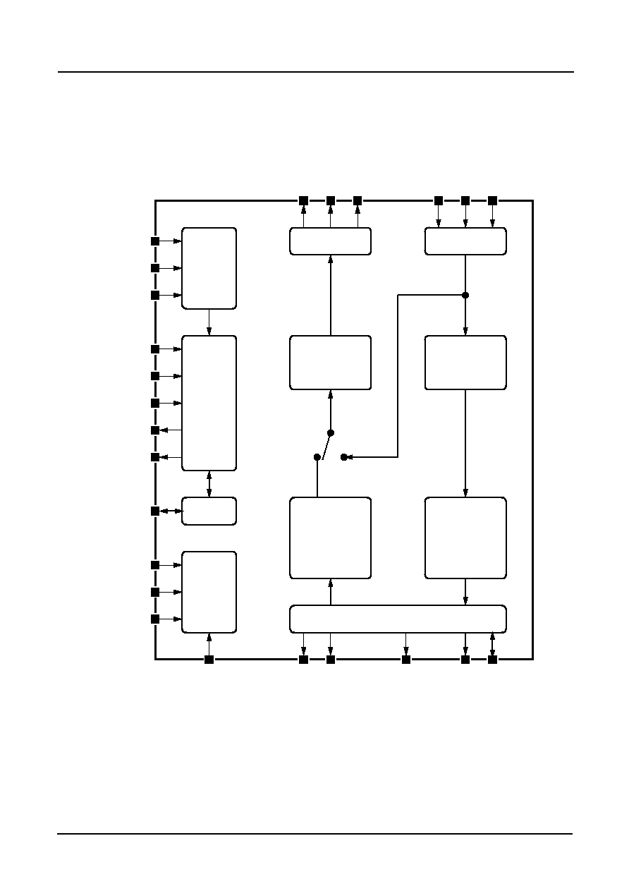
SM5904BF
Control
Input 1
Control
Input 2
Micro-
controller
Interface
General
Port
Output Interface
Input Interface
Attenuator
Input Buffer
Decoder
Encoder
4M DRAM / External DRAM Interface
YBLKCK
YFCLK
YFLAG
YMDATA
YMCLK
YMLD
ZSENSE
UC1 to UC4
YDMUTE
NRESET
NTEST1,2
CLK
NRAS
NCAS2
NWE
A0 to A9
D0 to D3
Through
Mode
Compression
Mode
ZLRCK
ZSCK
ZSRDATA
YLRCK
YSCK
YSRDATA
DIT
SM5904
Block diagram
NIPPON PRECISION CIRCUITS-11
SM5904BF
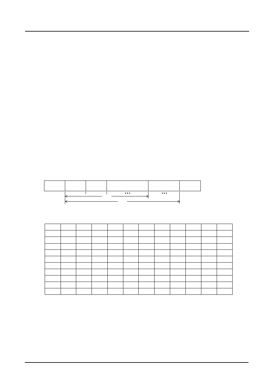
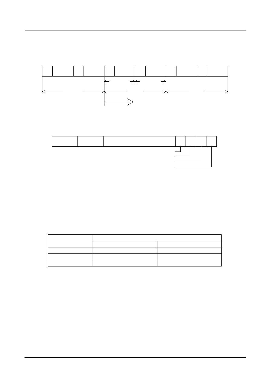
Write command format (Commands 80 to 86)
SM5904BF has two modes of operation; shock-
proof mode and through mode.
The operating sequences are controlled using com-
mands from a microcontroller.
D7
D6
D5
D4
D3
D2
D1
D0
B7
B6
B5
B4
B3
B2
B1
B0
COMMAND 8bit
DATA 8bit
YMDATA
YMCLK
YMLD
B7
B6
B5
B4
B3
B2
B1
B0
COMMAND 8bit
YMDATA
YMCLK
YMLD
S7
S6
S5
S4
S3
S2
S1
S0
STATUS 8bit
ZSENSE
B7
B6
B5
B4
B3
B2
B1
B0
COMMAND 8bit
YMDATA
YMCLK
YMLD
S7
S6
S1
S0
RESIDUAL DATA 16bit
ZSENSE
M1 M2
M7
M8
Functional description
Read command format (Command 92 (memory residual read))
Read command format (Commands 90, 91, 93)
Microcontroller interface
Commands from the microcontroller are input using
3-wire serial interface inputs; data (YMDATA), bit
clock (YMCLK) and load signal (YMLD).
In the case of a read command from the microcon-
troller, bit serial data is output (ZSENSE) synchro-
nized to the bit clock input (YMCLK).
Write command format (Commands 87)
D11 D10
D4
D3
D2
D1
D0
B7
B6
B5
B4
B3
B2
B1
B0
COMMAND 8bit
DATA 12bit
YMDATA
YMCLK
YMLD
NIPPON PRECISION CIRCUITS-12
SM5904BF
Bit
Name
Function
H operation
Reset level
D7
MSWREN
Encode sequence start/stop
Start
L
D6
MSWACL
Write address reset
Reset
L
D5
MSRDEN
Decode sequence start/stop
Start
L
D4
MSRACL
Read address reset
Reset
L
D3
MSDCN2
MSDCN2=H, MSDCN1=H: 3-pair comparison start
L
MSDCN2=H, MSDCN1=L: 2-pair comparison start
D2
MSDCN1
MSDCN2=L, MSDCN1=H: Direct-connect start
L
MSDCN2=L, MSDCN1=L: Connect operation stop
D1
WAQV
Q data valid
Valid
L
D0
MSON
Memory system ON
ON
L
1000 0000
B0
B1
B2
B3
B4
B5
B6
B7
80hex =
Shock-proof memory system settings
Bit
Name
Function
H operation Reset level
D7
D6
D5
D4
D3
UC4OE
Extension I/O port UC4 input/output setting
Output
L
D2
UC3OE
Extension I/O port UC3 input/output setting
Output
L
D1
UC2OE
Extension I/O port UC2 input/output setting
Output
L
D0
UC1OE
Extension I/O port UC1 input/output setting
Output
L
1000 0001
B0
B1
B2
B3
B4
B5
B6
B7
81hex =
Extension I/O port input/output settings
Bit
Name
Function
H operation Reset level
D7
D6
D5
D4
D3
UC4WD
Extension I/O port UC4 output data setting
H output
L
D2
UC3WD
Extension I/O port UC3 output data setting
H output
L
D1
UC2WD
Extension I/O port UC2 output data setting
H output
L
D0
UC1WD
Extension I/O port UC1 output data setting
H output
L
1000 0010
B0
B1
B2
B3
B4
B5
B6
B7
82hex =
Extension port HIGH/LOW output level
A port setting is invalid if that port has already been defined as an input using the 81H command above.
Command table
Write command summary
MS command 80
Extension I/O settings 81
Extension I/O output data settings 82
NIPPON PRECISION CIRCUITS-13
SM5904BF
Bit
Name
Function
H operation
Reset level
D7
ATT
Attenuator enable
Attenuator ON
L
D6
MUTE
Forced muting (changes instantaneously)
Mute ON
L
D5
SOFT
Soft muting (changes smoothly when ON only)
Soft mute
L
D4
NS
Includes noise shaper function when encoding
NS ON
L
D3
CMP12
12-bit comparison connect/ 16-bit comparison connect
12-bit comparison
L
D2
D1
D0
1000 0011
B0
B1
B2
B3
B4
B5
B6
B7
83hex =
Refer to "Attenuation", "Soft mute", "Force mute", "12-bit comparison connection".
Bit
Name
Function
H operation Reset level
D7
K7
MSB 2
L
D6
K6
2
H
D5
K5
2
L
D4
K4
2
L
D3
K3
2
L
D2
K2
2
L
D1
K1
2
L
D0
K0
LSB 2
L
1000 0100
B0
B1
B2
B3
B4
B5
B6
B7
84hex =
Refer to "Attenuation", "Soft mute", "Force mute".
-
1
-
2
-
3
-
4
-
5
-
6
-
7
-
8
Bit
Name
Function
H operation Reset level
D7
D6
RAMX2
External DRAM select
used
L
D5
YFLGS
FLAG6 set conditions (reset using status read command 90H)
L
- When YFLGS=0, YFCKP=0, YFCLK input falling edge, YFLAG=L
- When YFLGS=0, YFCKP=1, YFCLK input rising edge, YFLAG=L
D4
YFCKP
- When YFLGS=1, YFCKP=0, YFLAG=L
L
- When YFLGS=1, YFCKP=1, YFLAG=H
D3
COMPFB
Full-bit compression mode
L
D2
COMP6B
6-bit compression mode
H
D1
COMP5B
5-bit compression mode
L
D0
COMP4B
4-bit compression mode
L
1000 0101
B0
B1
B2
B3
B4
B5
B6
B7
85hex =
When the number of compression bits is set incorrectly (2 or more bits in D0 to D3 are set to 1 or all bits are set to 0),
6-bit compression mode is selected.
ATT, MUTE settings 83
Attenuation level settings 84
Option settings 85
NIPPON PRECISION CIRCUITS-14
SM5904BF
Digital Audio Interface settings 86
Sub code Q data settings 87
Bit
Name
Function
H operation Reset level
D7
CP1
Channel status and clock accuracy setting
L
CP1= 0, CP2= 0 Level 2 (max ± 300 ppm)
D6
CP2
CP1= 0, CP2= 1 Level 3 (max ± 10 %)
L
CP1= 1, CP2= 0 Level 1 (max ± 50 ppm)
CP1= 1, CP2= 1 Not supported
D5
LBIT
Digital audio signal generation logic. 0 = post-recording software
Unassigned
L
D4
DIT
Digital audio interface (DIT) enable. 0 = DIT output LOW
DIT= ON
L
D3
D2
D1
D0
1000 0110
B0
B1
B2
B3
B4
B5
B6
B7
86hex =
Bit
Name
Function
H operation Reset level
D11
QAD3
Q data setting and word address specification
L
D10
QAD2
QAD3 (MSB) to QAD0 (LSB) specify one of 10 valid addresses in the range 0000 to 1001.
L
D9
QAD1
* If an address in the range 1010 to 1111 is specified, the data on QD7 to QD0 is ignored.
L
D8
QAD0
Note that writing to address 1001 also functions as the write stop command.
L
D7
QD7
Q data setting ward data
Indefined
D6
QD6
Q data setting ward data
Indefined
D5
QD5
Q data setting ward data
Indefined
D4
QD4
Q data setting ward data
Indefined
D3
QD3
Q data setting ward data
Indefined
D2
QD2
Q data setting ward data
Indefined
D1
QD1
Q data setting ward data
Indefined
D0
QD0
Q data setting ward data
Indefined
1000 0111
B0
B1
B2
B3
B4
B5
B6
B7
87hex =
MSB
LSB
QAD3
QAD2
QAD1
QAD0
QD7
QD6
QD5
QD4
QD3
QD2
QD1
QD0
0
0
0
0
CTL0
CTL1
CTL2
CTL3
ADR3
ADR2
ADR1
ADR0
0
0
0
1
DQ1
DQ2
DQ3
DQ4
DQ5
DQ6
DQ7
DQ8
0
0
1
0
DQ9
DQ10
DQ11
DQ12
DQ13
DQ14
DQ15
DQ16
0
0
1
1
DQ17
DQ18
DQ19
DQ20
DQ21
DQ22
DQ23
DQ24
0
1
0
0
DQ25
DQ26
DQ27
DQ28
DQ29
DQ30
DQ31
DQ32
0
1
0
1
DQ33
DQ34
DQ35
DQ36
DQ37
DQ38
DQ39
DQ40
0
1
1
0
DQ41
DQ42
DQ43
DQ44
DQ45
DQ46
DQ47
DQ48
0
1
1
1
DQ49
DQ50
DQ51
DQ52
DQ53
DQ54
DQ55
DQ56
1
0
0
0
DQ57
DQ58
DQ59
DQ60
DQ61
DQ62
DQ63
DQ64
1
0
0
1
DQ65
DQ66
DQ67
DQ68
DQ69
DQ70
DQ71
DQ72
When shockproof mode is ON, the Q data is specified according to the data output from the SM5904BF.
Adderss map for Q data setting beuffer
NIPPON PRECISION CIRCUITS-15
SM5904BF
Bit
Name
Function
HIGH-level state
S7
FLAG6
Signal processor IC jitter margin exceeded
Exceeded
S6
MSOVF
Write overflow (Read once only when RA exceeds WA)
DRAM overflow
S5
BOVF
Input buffer memory overflow
Input buffer memory overflow
because sampling rate of input data is too fast
S4
S3
DCOMP
Data compare-connect sequence operating
Compare-connect sequence operating
S2
MSWIH
Encode sequence stop due to internal factors
Encoding stopped
S1
MSRIH
Decode sequence stop due to internal factors
Decoding stopped
S0
1001 0000
B0
B1
B2
B3
B4
B5
B6
B7
90hex =
Refer to "Status flag operation summary".
Bit
Name
Function
HIGH-level state
S7
MSEMP
Valid data empty state (Always HIGH when RA exceeds VWA)
No valid data
S6
OVFL
Write overflow state (Always HIGH when WA exceeds RA)
Memory full
S5
ENCOD
Encode sequence operating state
Encoding
S4
DECOD
Decode sequence operating state
Decoding
S3
QRDY
Subcode Q data write-buffer write enable
Write enabled
S2
S1
S0
1001 0001
B0
B1
B2
B3
B4
B5
B6
B7
91hex =
Refer to "Status flag operation summary".
Read command summary
Shock-proof memory status (1) 90
Shock-proof memory status (2) 91
NIPPON PRECISION CIRCUITS-16
SM5904BF
Bit
Name
Function
HIGH-level state
S7
S6
S5
S4
S3
UC4RD
S2
UC3RD
S1
UC2RD
S0
UC1RD
1001 0011
B0
B1
B2
B3
B4
B5
B6
B7
93hex =
Input data entering (or output data from) an extension port terminal is echoed to the microcontroller.
(That is, the input data entering an I/O port configured as an input port using the 81H command,
OR the output data from a pin configured as an output port using the 82H command.)
Bit
Name
Function
S7
AM21
Valid data accumulated VWA-RA (MSB) 8M bits
S6
AM20
S5
AM19
S4
AM18
S3
AM17
S2
AM16
S1
AM15
S0
AM14
M1
AM13
M2
AM12
M3
AM11
M4
AM10
M5
AM09
M6
AM08
M7
AM07
M8
AM06
1001 0010
B0
B1
B2
B3
B4
B5
B6
B7
92hex =
Note. The time conversion factor varies depending on the compression bit mode.(M = 1,048,576 K= 1,024)
Residual time (sec) = Valid data residual (Mbits)
◊
Time conversion value K
where the Time conversion value K (sec/Mbit)
2.78(4 bits), 2.22 (5 bits), 1.85 (6 bits) and 0.74 (Full bits).
4M bits
2M bits
1M bits
512k bits
256k bits
128k bits
64k bits
32k bits
16k bits
8k bits
1k bits
4k bits
2k bits
512 bits
256 bits
Shock-proof memory valid data residual 92
Extension I/O inputs 93
NIPPON PRECISION CIRCUITS-17
SM5904BF
Status flag operation summary
Flag
Read
name
method
FLAG6
READ
Meaning
- Indicates to the CD signal processor DSP (used for error correction, de-interleaving) that a
90H
disturbance has exceeded the RAM jitter margin.
bit 7
Set
- Set according to the YFLAG input and the operating state of YFCKP and YFLGS.
FLAG6 set conditions
When YFLGS=0, YFCKP=0, YFCLK input falling edge, YFLAG=Low
When YFLGS=0, YFCKP=1, YFCLK input rising edge, YFLAG=Low
When YFLGS=1, YFCKP=0, YFLAG=Low
When YFLGS=1, YFCKP=1, YFLAG=High
Reset
- By 90H status read
- By 80H command when MSON=ON
- After external reset
MSOVF
READ
Meaning
- Indicates once only that a write to external DRAM has caused an overflow. (When reset
90H
by the 90H status read command, this flag is reset even if the overflow condition continues.)
bit 6
Set
- When the write address (WA) exceeds the read address (RA)
Reset
- By 90H status read
- When a read address clear (MSRACL) or write address clear (MSWACL) command is issued
- After external reset
BOVF
READ
Meaning
- Indicates input data rate was too fast causing buffer overflow and loss of data
90H
Set
- When inputs a data during a buffer memory overflow
bit 5
Reset
- By 90H status read
- When a read address clear (MSRACL) or write address clear (MSWACL) command is issued
- After external reset
DCOMP
READ
Meaning
- Indicates that a compare-connect sequence is operating
90H
Set
- When a (3-pair or 2-pair) compare-connect start command is received (MSDCN2=1)
bit 3
- When a direct connect command is received (MSDCN2=0, MSDCN1=1)
Reset
- When a (3-pair or 2-pair) comparison detects conforming data
- When the connect has been performed after receiving a direct connect command
- When a compare-connect stop command (MSDCN2=0, MSDCN1=0) is received
- When a MSWREN=1 command is received (However, if a compare-connect command is
received at the same time, the compare-connect command has priority.)
- After external reset
MSWIH
READ
Meaning
- Indicates that the encode sequence has stopped due to internal factors
90H
(not microcontroller commands)
bit 2
Set
- When FLAG6 (above) is set
- When BOVF (above) is set
- When MSOVF (above) is set
Reset
- When conforming data is detected after receiving a compare-connect start command
- When the connect has been performed after receiving a direct connect command
- When a read address clear (MSRACL) or write address clear (MSWACL) command is received
- After external reset
MSRIH
READ
Meaning
- Indicates that the decode sequence has stopped due to internal factors
90H
(not microcontroller commands)
bit 1
Set
- When the valid data residual becomes 0
Reset
- By 90H status read
- When a read address clear (MSRACL) or write address clear (MSWACL) command is issued
- After external reset
NIPPON PRECISION CIRCUITS-18
SM5904BF
Flag
Read
name
method
MSEMP
READ
Meaning
- Indicates that the valid data residual has become 0
91H
Set
- When the VWA (final valid data's next address)
bit 7
= RA (address from which the next read would take place)
Reset
- Whenever the above does not apply
OVFL
READ
Meaning
- Indicates a write to external DRAM overflow state
91H
Set
- When the write address (WA) exceeds the read address (RA).
bit 6
(Note: This flag is not set when WA=RA through an address initialize or reset operation.)
Reset
- When the read address (RA) is advanced by the decode sequence
- When a read address clear (MSRACL) or write address clear (MSWACL) command is issued
- After external reset
ENCOD
READ
Meaning
- Indicates that the encode sequence (input data entry, encoding, DRAM write) is operating
91H
Set
- By the 80H command when MSWREN=1
bit 5
- When conforming data is detected during compare-connect operation
- When the connect has been performed after receiving a direct connect command
Reset
- When the FLAG6 flag=1 (above)
- When the OVFL flag=1 (above)
- By the 80H command when MSWREN=0
- By the 80H command when MSDCN1=1 or MSDCN2=1 (compare-connect start command)
- By the 80H command when MSON=0
- After external reset
Note. Reset conditions have priority over set conditions. For example, if the 80H command has
MSWREN=1 and MSDCN1=1, the ENCOD flag is reset and compare-connect operation starts.
DECOD
READ
Meaning
- Indicates that the decode sequence (read from DRAM, decoding,
91H
attenuation, data output) is operating
bit 4
Set
- By a new 80H command when MSRDEN=1 and the MSEMP flag=0 (above)
Reset
- Whenever the above does not apply
QRDY
READ
Meaning
Subcode Q data write-buffer write enable indicator
91H
Set
After internal subcode Q data write-buffer contents are read out.
bit 3
Reset
When data is written to address 1001 using the 87H command.

NIPPON PRECISION CIRCUITS-19
SM5904BF
- MSWREN
When 1: Encode sequence starts
Invalid when MSON is not 1 within the
same 80H command
Invalid when FLAG6=1
Invalid when OVFL=1
Invalid when a compare-connect start
command (MSDCN2=1 or MSDCN1=1)
occurs simultaneously
Direct connect if a compare-connect
sequence is already operating
When 0: Encode sequence stops
- MSWACL
When 1: Initializes the write address (WA)
When 0: No operation
- MSRDEN
When 1: Decode sequence starts
Does not perform decode sequence if
MSON=1.If there is no valid data, decode
sequence temporarily stops. But, because
the MSRDEN flag setting is maintained as
is, the sequence automatically re-starts
when valid data appears.
When 0: Decode sequence stops
-MSRACL
When 1: Initializes the read address (RA)
When 0: No operation
- MSDCN2, MSDCN1
When 1 and 1: 3-pair compare-connect sequence
starts
When 1 and 0: 2-pair compare-connect sequence
starts
When 0 and 1: Direct connect sequence starts
When 0 and 0: Compare-connect sequence stops.
No operation if a compare-connect
sequence is not operating.
- WAQV
When 1: The immediately preceding YBLKCK
falling-edge timing WA (write address)
becomes the VWA (valid write address).
When 0: No operation
- MSON
When 1: Memory system turns ON and shock-
proof operation starts
When 0: Memory system turns OFF and through-
mode playback starts. (In this mode, the
attenuator is still active.)
Write command supplementary information
80H (MS command)
81H (Extension I/O port settings)
82H (Extension I/O port output data settings)

NIPPON PRECISION CIRCUITS-20
SM5904BF
85H (option settings)
- RAMX2
When 1: Uses 2 DRAMs (use external DRAM)
When 0: Uses a single DRAM (internal only)
- YFLGS, YFCKP
When 0 and 0: Sets FLAG6 on the falling edge of
YFCLK when YFLAG=0
When 0 and 1: Sets FLAG6 on the rising edge of
YFCLK when YFLAG=0
When 1 and 0: Sets FLAG6 when YFLAG=0
When 1 and 1: Sets FLAG6 when YFLAG=1
- COMPFB, COMP6B, COMP5B, COMP4B
When 0, 0, 0 and 1: Selects 4-bit compression
mode
When 0, 0, 1 and 0: Selects 5-bit compression
mode
When 1, 0, 0 and 0: Selects full-bit compression
mode
In all other cases: Selects 6-bit compression mode
Changing mode without initializing during opera-
tion is possible.
83H (ATT, MUTE, 12-bit comparison connection settings)
- ATT (attenuator enable)
When 1: Attenuator settings become active (84H
command)
When 0: Attenuator settings become inactive, and
output continues without attenuation
- MUTE (forced muting)
When 1: Outputs are instantaneously muted to
0.(note 1)
Same effect as taking the YDMUTE pin
HIGH.
When 0: No muting(note 1)
(note1) Effective at the start of left-channel output
data.
- SOFT (soft muting)
When 1: Outputs are smoothly muted to 0.
When 0: No muting.
Soft mute release occurs instantaneously
to either the value set by the 84H com-
mand (When ATT=1) or 0dB (When
ATT=0)
- MUTE, SOFT, YDMUTE relationship
When all mute inputs are 0, mute is released.
- NS (noise shaper enable)
When 1: Includes noise shaper function in com-
pression-mode shockproof operation.
When 0: Performs comparison connection using
all 16 bits of input data.
- CMP12 (12-bit comparison connection)
When 1: Performs comparison connection using
only the most significant 12 bits of input
data.
When 0: Performs comparison connection using
all 16 bits of input data.
NIPPON PRECISION CIRCUITS-21
SM5904BF
86H (digital audio interface settings)
- CP1, CP2 (channel status and clock accuracy set-
ting)
When 0 and 0: Level 2 (max ± 300 ppm)
When 0 and 1: Level 3 (max ± 10%)
When 1 and 0: Level 1 (max ± 50 ppm)
When 1 and 1: Not supported
- LBIT (digital audio signal generation logic)
When 1: Not assigned
When 0: Post-recording software
- DIT (digital audio interface enable)
When 1: DIT output enable
When 0: DIT LOW-level output
87H (subcode Q data setting)
- QAD3 to QAD0 (Q data setting and word address
specification)
QAD3 (MSB) to QAD0 (LSB) specify one of 10
valid addresses in the range 0000 to 1001.
If an address in the range 1010 to 1111 is speci-
fied, the data on QD7 to QD0 is ignored.
Note that writing to address 1001 also functions
as the write stop command.
- QD7 to QD0 (Q data setting and word data)
The CD Q-channel has the general data format
shown below.
The write data required to fully specify the Q data
is the 80 bits comprising CONTROL, ADR, and
DATA-Q.
The CRC write data is not required because it is
generated by recalculation.
Control
0
1
2
3
4
5
6
7
8
9
78 79 80
95
S0, S1
ADR
DATA-Q
CRC
S0, S1
96 bit
80 bit
bit
QAD3
QAD2
QAD1
QAD0
QD7
QD6
QD5
QD4
QD3
QD2
QD1
QD0
0
0
0
0
CTL0
CTL1
CTL2
CTL3
ADR3
ADR2
ADR1
ADR0
0
0
0
1
DQ1
DQ2
DQ3
DQ4
DQ5
DQ6
DQ7
DQ8
0
0
1
0
DQ9
DQ10
DQ11
DQ12
DQ13
DQ14
DQ15
DQ16
0
0
1
1
DQ17
DQ18
DQ19
DQ20
DQ21
DQ22
DQ23
DQ24
0
1
0
0
DQ25
DQ26
DQ27
DQ28
DQ29
DQ30
DQ31
DQ32
0
1
0
1
DQ33
DQ34
DQ35
DQ36
DQ37
DQ38
DQ39
DQ40
0
1
1
0
DQ41
DQ42
DQ43
DQ44
DQ45
DQ46
DQ47
DQ48
0
1
1
1
DQ49
DQ50
DQ51
DQ52
DQ53
DQ54
DQ55
DQ56
1
0
0
0
DQ57
DQ58
DQ59
DQ60
DQ61
DQ62
DQ63
DQ64
1
0
0
1
DQ65
DQ66
DQ67
DQ68
DQ69
DQ70
DQ71
DQ72
Adderss map for Q data setting beuffer
- Subcode Q data setting process
Initially, data is written to word address range
0000 to 1000, and then data is written to address
1001. Next, only data that needs to be changed
is written if the 91H command QRDY bit is 1, and
then address 1001 is written again. Note that
when shockproof mode is ON, the Q data is
specified according to the data output from the
SM5904BF.

NIPPON PRECISION CIRCUITS-22
SM5904BF
Shock-proof mode is the mode that realizes shock-
proof operation using DRAM. Shock-proof mode is
invoked by setting MSON=H in microcontroller
command 80H.
This mode comprises the following 3 sequences.
Shock-proof operation overview
- Encode sequence
1. Input data from a signal processor IC is stored in
internal buffers.
2. Encoder starts after a fixed number of data have
been received.
3. The encoder, after the most suitable predicting
filter type and quantization steps have been deter-
mined, performs ADPCM encoding and then writes
to DRAM.
- Decode sequence
1. Reads compressed data stored in external buffer
RAM at rate fs.
2. Decoder starts, using the predicting filter type
and quantization levels used when encoded.
3. Performs attenuation operation (including muting
operation)
4. Outputs the result.
- Compare-connect sequence
1. Encoding immediately stops when either external
buffer RAM overflows or when a CD read error
occurs due to shock vibrations.
2. Then, using microcontroller command 80H, the
compare-connect start command is executed and
compare-connect sequence starts.
3. Compares data re-read from the CD with the pro-
cessed final valid data stored in RAM (confirms its
correctness).
4. As soon as the comparison detects conforming
data, compare-connect sequence stops and
encode sequence re-starts, connecting the data
directly behind previous valid data.
NIPPON PRECISION CIRCUITS-23
SM5904BF
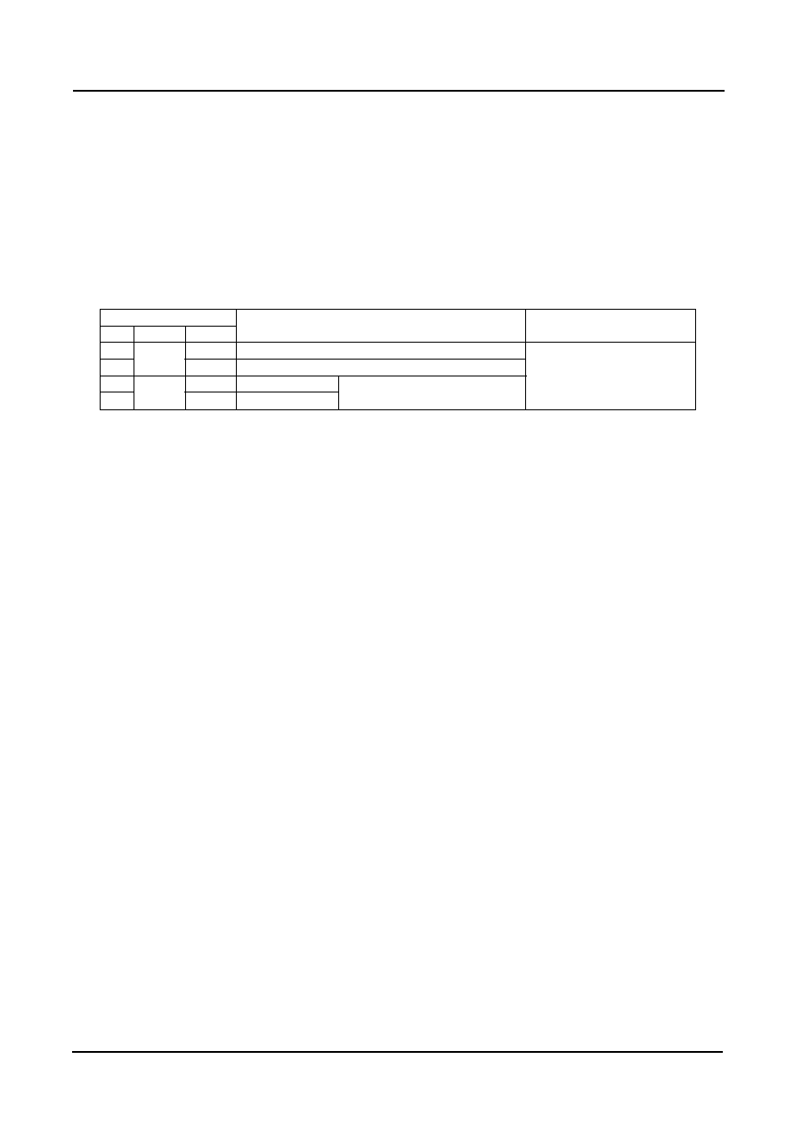
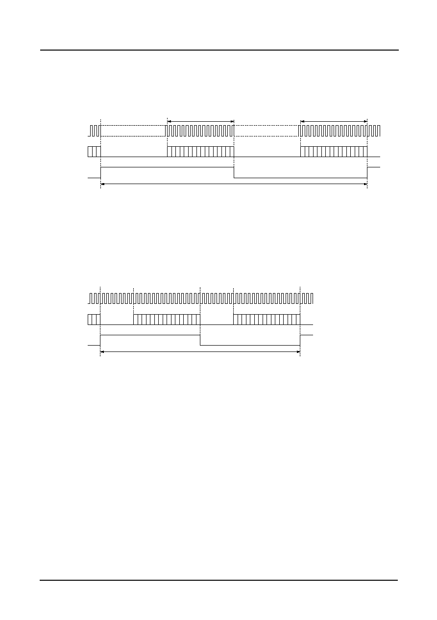
13.3ms
VWA latch set
WAQV set
VWA(x)
VWA(x + 1)
YBLKCK
Microcontroller data set
Refer to Microcontroller interface
VWA
Values shown are for rate fs. The values are 1/2 those shown at rate 2fs.
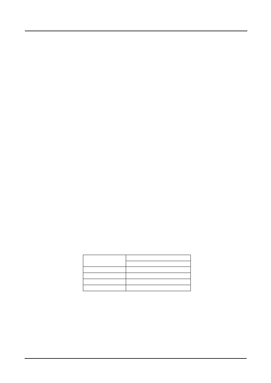
Fig 2. YBLKCK and VWA relationship
The VWA is determined according to the YBLKCK
pin and WAQV command. Refer to the timing chart
below.
1.YBLKCK is a 75 Hz clock(HIGH for 136
µ
s) when
used for normal read mode and it is a 150 Hz clock
when used for double-speed read mode, synchro-
nized to the CD format block end timing.
When this clock goes LOW, WA which is the write
address of internal encode sequence, is stored
(see note 2).
2.The microcontroller checks the subcode and, if
confirmed to be correct, generates a WAQV com-
mand (80H).
3.When the WAQV command is received, the previ-
ously latched WA is stored as the VWA.
(note 2) Actually, there is a small time difference, or
gap, between the input data and YBLKCK. This gap
serves to preserves the preceding WA to protect
against incorrect operation.
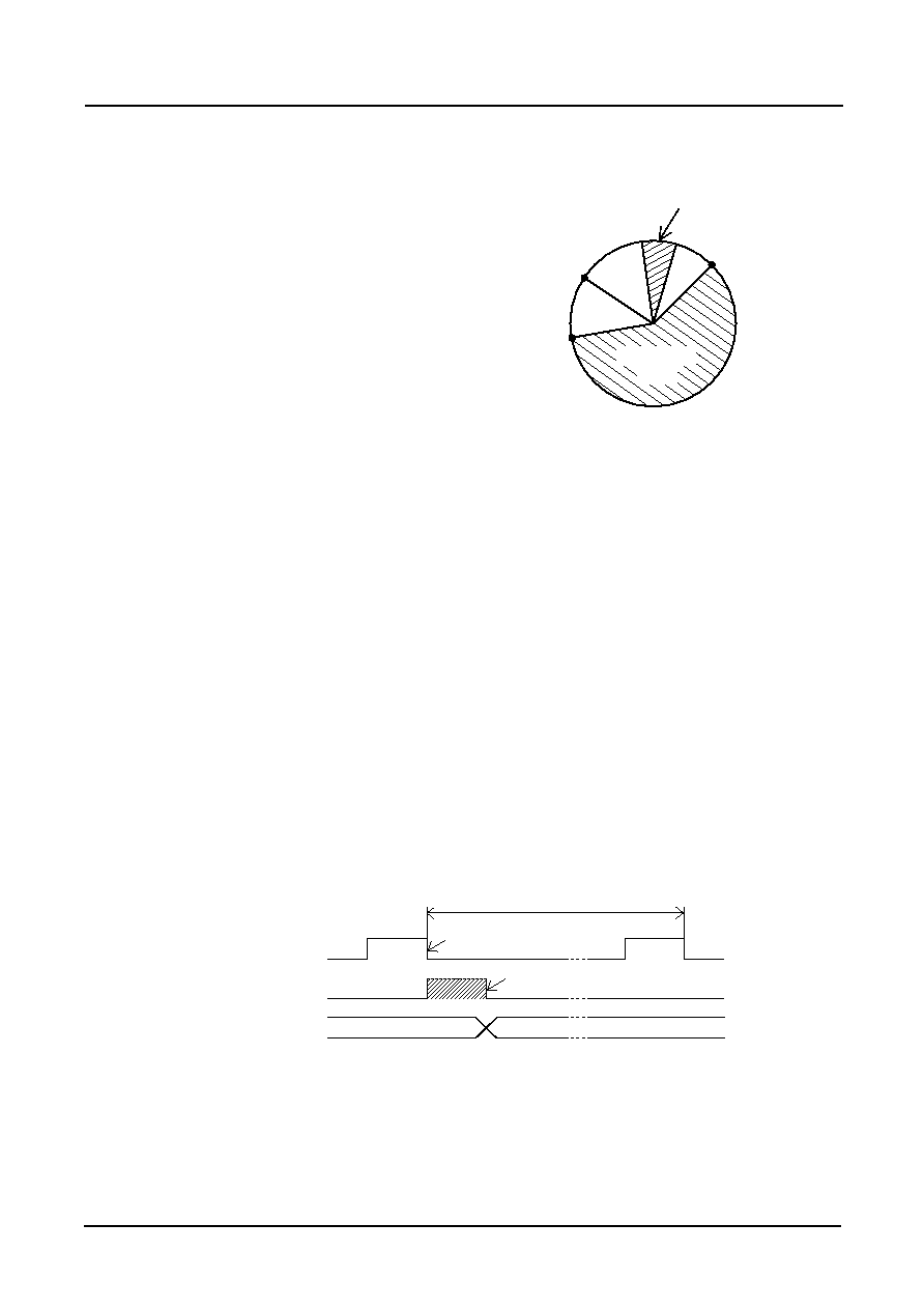
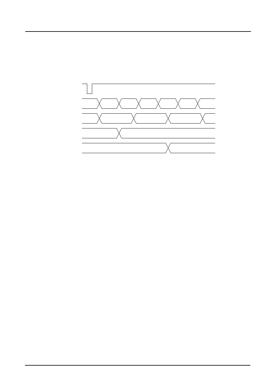
RAM addresses
The SM5904BF has a 4M DRAM as the internal
buffer and an external 4M DRAM can be also con-
nected to expand the memory to 4M bits.
Three kinds of addresses are used for external
RAM control.
WA (write address)
RA (read address)
VWA (valid write address)
Among these, VWA is the write address for con-
forming data whose validity has been confirmed.
Determination of the correctness of data read from
the CD is delayed relative to the encode write pro-
cessing, so VWA is always delayed relative to WA.
The region available for valid data is the area
between VWA-RA.
- Connect data work area
This is an area of memory reserved for connect
data. This area is 4k bits.
Fig 1. RAM addresses
RA
WA
VWA
Valid data
area
Connect data work area
VWA (valid write address)
NIPPON PRECISION CIRCUITS-24
SM5904BF
Correct data demodulation becomes impossible for
the CD signal processor IC when a disturbance
exceeding the RAM jitter margin occurs. The
YFLAG signal input pin is used to indicate when
such a condition has occurred.
The YFCLK is a 7.35 kHz clock synchronized to the
CD format frame 1.
The IC checks the YFLAG input and stops the
encode sequence when such a disturbance has
occurred, and then makes FLAG6 active.
The YFLAG check method used changes depend-
ing on the YFLGS flag and YFCKP flag (85H com-
mand). See table1.
If YFLAGS is set to 1, then YFCLK should be tied
either High or Low.
YFLAG, YFCLK, FLAG6
85H command
YFLGS
YFCKP
FLAG6 set conditions
FLAG6 reset conditions
1
0
0
When YFLAG=LOW on YFCLK input falling edge
- By status read (90H command)
2
1
When YFLAG=LOW on YFCLK input rising edge
- When MSON=LOW
3
1
0
When YFLAG=LOW
YFCLK be tied either High or Low
- After system reset
4
1
When YFLAG=HIGH
Table 1. YFLAG signal check method

NIPPON PRECISION CIRCUITS-25
SM5904BF
Compare-connect sequence
The SM5904BF supports three kinds of connect
modes; 3-pair compare-connect, 2-pair compare-
connect and direct connect.
Note that the SM5904BF can also operate in 12-bit
comparison connect mode using only the most sig-
nificant 12 bits of data for connection operation.
In 3-pair compare-connect mode, the final 6 valid
data (3 pairs of left- and right-channel data input
before encode processing) and the most recently
input data are compared until three continuous data
pairs all conform. At this point, the encode
sequence is re-started and data is written to VWA.
In 2-pair compare-connect mode, comparison
occurs just as for 3-pair comparison except that
only 2 pairs from the three compared need to con-
form with the valid data. At this point, the encode
sequence is re-started and data is written to VWA.
In direct-connect mode, comparison is not per-
formed at all, and encode sequence starts and data
is written to the VWA. This mode is for systems that
cannot perform compare-connect operation.
- Compare-connect preparation time
1. Comparison data preparation time
Internally, when the compare-connect start com-
mand is issued, a sequence starts to restore the
data for comparison. The time required for this
preparation after receiving the command is approxi-
mately 2.5
◊
(1/fs). (approximately 60
µ
s when fs =
44.1 kHz)
2. After the above preparation is finished, data is
input beginning from the left-channel data and com-
parison starts.
3. If the compare-connect command is issued
again, the preparation time above is not necessary
and operation starts from step 2.
4. The same sequence takes place in direct-con-
nect mode also. However, at the point when 3
words have been input, all data is directly connect-
ed as if comparison and conformance had taken
place.
- Compare-connect sequence stop
If a compare-connect stop command (80H with
MSDCN1= 1, MSDCN2= 0) is input from the micro-
controller, compare-connect sequence stops.
If compare-connect sequence was not operating,
the compare-connect stop command performs no
operation. However, make sure that the other bit
settings within the same 80H command are valid.
NIPPON PRECISION CIRCUITS-26
SM5904BF
- DRAM initialization refresh
A 15-cycle RAS-only refresh is carried out for
DRAM initialization under the following conditions.
When MSON changes from 0 to 1 using command
80H.
When from MSON=1, MSRDEN=0 and
MSWREN=0 states only MSWREN changes to 1.
In this case, encode sequence immediately starts
and initial data is written (at 2fs rate input) after a
delay of 0.7ms.
- Refresh during Shock-proof mode operation
In this IC, a data access operation to any address
also serves as a data refresh. Accordingly, there
are no specific refresh cycles other than the initial-
ization refresh cycle (described above).
This has the resulting effect of saving on DRAM
power dissipation.
A data access to DRAM can occur in an encode
sequence write operation or in a decode sequence
read operation. Write sequence write operation
stops during a connect operation whereas a read
sequence read operation always continues while
data is output to the D/A. The refresh rate for each
DRAM during decode sequence is shown in the
table below.
The decode sequence, set by MSON=1 and MSR-
DEN=1, operates when valid data is in DRAM
(when MSEMP=0).
- When MSON=0, DRAM is not refreshed because
no data is being accessed. Although MSON=1,
DRAM is not refreshed if ENCOD=0 and DECOD=0
(both encode and decode sequence are stopped).
DRAM refresh
Table 2. Decode sequence refresh rate
DRAMs used (same for 1 or 2 DRAMs)
Data compression mode
4M (1M
◊
4 bits)
4 bit
10.88 ms
5 bit
8.71 ms
6 bit
7.26 ms
Full bit
2.72 ms
Encode sequence temporary stop
- When RAM becomes full, MSWREN is set LOW
using the 80H command and encode sequence
stops. (For details of the stop conditions, refer to
the description of the ENCOD flag.)
- Then, if MSWREN is set HIGH without issuing a
compare-connect start command, the encode
sequence re-starts. At this time, new input data is
written not to VWA, but to WA. In this way, the data
already written to the region between VWA and WA
is not lost.
- But if the MSWREN is set HIGH (80H command)
after using the compare-connect start command
even only once, data is written to VWA. If data is
input before comparison and conformance is
detected, the same operation as direct-connect
mode takes place when the command is issued.
After comparison and conformance are detected,
no operation is performed because the encode
sequence has already been started. However,
make sure that the other bit settings within the
same 80H command are valid.
NIPPON PRECISION CIRCUITS-27
SM5904BF
WA CAS
RA CAS
Encode compression mode
Decode compression mode
3FE
3FF
001
002
004
005
3FD
3FE
3FF
001
002
A
YMLD
When 85H generated
A
B
B
003
Selecting compression mode
Even when the compression mode in selected with
the 85H command during shock-proof operation,no
malfunction occurs.
The compression mode change is not performed
immediately after input of the 85H command, but it
is performed at the following timing.
(note) CAS-000 is connect data.
NIPPON PRECISION CIRCUITS-28
SM5904BF
Through-mode operation
If MSON is set LOW (80H command), an operating
mode that does not perform shock-proof functions
becomes active. In this case, input data is passed
as-is (after attenuator and mute operations) to the
output. External DRAM is not accessed.
- In this case, input data needs to be at a rate fs
and the input word clock must be synchronized to
the CLK input (384fs). However, short-range jitter
can be tolerated (jitter-free system).
- Jitter-free system timing starts from the first
YLRCK rising edge after either (A) a reset (NRE-
SET= 0) release by taking the reset input from
LOW to HIGH or (B) by taking MSON from HIGH to
LOW. Accordingly, to provide for the largest possi-
ble jitter margin, it is necessary that the YLRCK
clock be at rate fs by the time jitter-free timing
starts.
The jitter margin is 0.2/ fs (80 clock cycles).
This jitter margin is the allowable difference
between the system clock (CLK) divided by 384 (fs
rate clock) and the YLRCK input clock.
If the timing difference exceeds the jitter margin,
irregular operation like data being output twice or,
conversely, incomplete data output may occur. In
the worst case, a click noise may also be generat-
ed.
When switching from shock-proof mode to through
mode, an output noise may be generated, and it is
therefore recommended to use the YDMUTE set-
ting to mute ZSRDATA until just before data output.
- The attenuation register is set by the 84H com-
mand.
- The attenuation register set value becomes active
when the 83H command sets the ATT flag to 1.
When the ATT flag is 0, the attenuation register
value is considered to be the equivalent of 256 for a
maximum gain of 0 dB.
- The gain (dB) is given from the set value (Datt)
by the following equation.
Gain = 20
◊
log(Datt/256) [dB]; left and right chan-
nels
- For the maximum attenuation register set value
(Datt = 255), the corresponding gain is -0.03 dB.
But when the ATT flag is 0 (Datt = 256), there is no
attenuation.
- After a system reset initialization, the attenuation
register is set to 64 (-12 dB). However, because the
ATT flag is reset to 0, there is no attenuation.
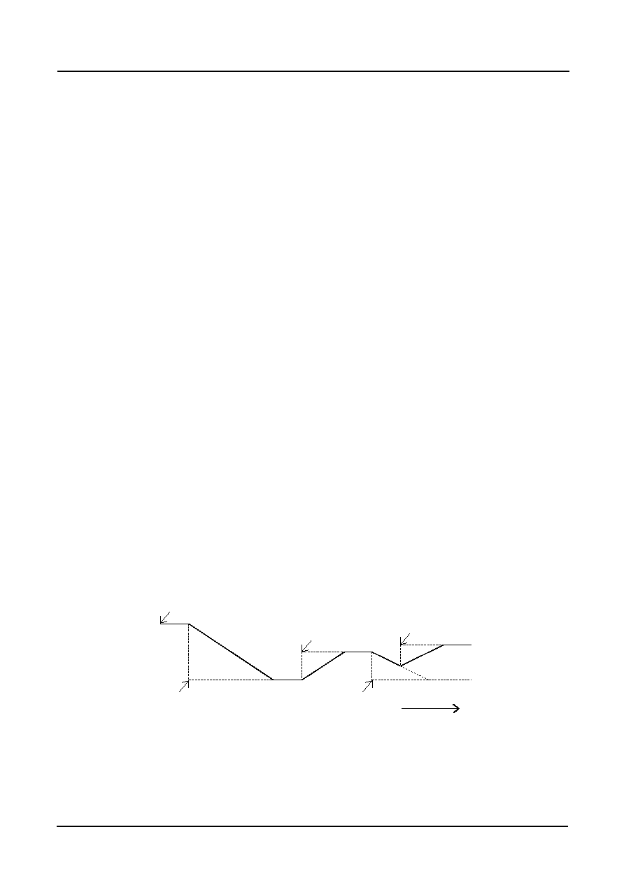
- When the attenuation register setting changes or
when the ATT flag changes, the gain changes
smoothly from the previous set gain towards the
new set value. If a new value for the attenuation
level is set before the previously set level is
reached, the gain changes smoothly towards the
latest setting.
The gain changes at a rate of 4
◊
(1/fs) per step. A
full-scale change (255 steps) takes approximately
23.3 ms (when fs = 44.1 kHz). See fig 3.
Attenuation
Fig 3. Attenuation operation example
set 3
Gain
set 5
set 1
set 4
set 2
time
NIPPON PRECISION CIRCUITS-29
SM5904BF
Force mute
Soft mute
Soft mute operation is controlled by the SOFT flag
using a built-in attenuation counter.
Mute is ON when the SOFT flag is 1. When ON, the
attenuation counter output decrement by 1 step at a
time, thereby reducing the gain. Complete mute
takes 1024/fs (or approximately 23.2 ms for fs =
44.1 kHz).
Conversely, mute is released when the SOFT flag
is 0. In this case, the attenuation counter instanta-
neously increases. The attenuation register takes
on the value when the ATT flag was 1. If the ATT
flag was 0, the new set value is 256 (0 dB).
Fig 4. Soft mute operation example
256 step
/ 1024T
S
SOFT
Attenation level
or full scale
-
(Gain)
Serial output data is muted by setting the YDMUTE
pin input HIGH or by setting the MUTE flag to 1.
Mute starts and finishes on the leading left-channel
bit.
When MSON is HIGH and valid data is empty
(MSEMP=H), the output is automatically forced into
the mute state.
12-bit comparison connection
When the CMP12 flag is set to 1, the least signifi-
cant 4 bits of the 16-bit comparison connection
input data are discarded and comparison connec-
tion is performed using the remaining 12 bits.
Note that if the CMP12 flag is set to 1 during a com-
parison connection operation, only the most signifi-
cant 12 bits are used for comparison connection
from that point on.
NIPPON PRECISION CIRCUITS-30
SM5904BF
Digital audio interface
When the DIT flag is set to 1, the digital audio inter-
face output from pin DIT is enabled. The output
data structure is modulated using a preamble and
biphase mark encoding.
Figure 5. Frame format
Figure 6. Subframe format
Channel 2
M
Channel 1
W
B
W
M
W
Frame 0
Frame 191
Channel 2
Channel 1
Channel 2
Channel 1
Frame 1
Frame 0
Sub Frame
Sub Frame
Start Block
Auxiliary
Preamble
Audio Sample Word
V
U
C
P
0
3 4
7 8
27
28
31
LSB
MSB
LSB
Validity Flag
User Data
Channel Status
Parity Bit
Preamble
Channel coding
Leading symbol = 0
Leading symbol = 1
B
11101000
00010111
M
11100010
00011101
W
11100100
00011011
The SM5904BF starts with 0, so only the preamble patterns for leading symbol = 0 are used.
Preamble
The preamble is a particular bit pattern used to per-
form subframe and block synchronization and dis-
crimination, assigned to one of 4 time slot divisions
(0 to 3), comprising 8 continuous biphase modulat-
ed transfer rate status indicators.
There are 3 types of preamble. The leading pream-
ble pattern of all blocks is preamble pattern B,
which is then followed by preamble pattern M for
channel 1, and preamble pattern W for channel 2.
Digital audio sample data and auxiliary audio
The digital audio sample data is a 20-bit digitized
audio signal. Auxiliary audio data, on the other
hand, can be audio sample data of varying length.
The SM5904BF uses a 16-bit audio data structure
internally with audio data output bits 4 to 11 set to 0
and bits 12 to 27 output in LSB first format.
Audio sample validity
The validity flag is set to 0 when the digital audio
sample data is output correctly, or it is set to 1 if the
output is incorrect. It is also set to 1 if encoding
does not start when the device is operating in
forced mute, microcontroller forced mute, and
shockproof mode.
NIPPON PRECISION CIRCUITS-31
SM5904BF
User bit data
User bit data is data specified by the user. The data
is output, after the Q data has been specified, in the
following sequence.
0
1
2
3
4
5
6
7
8
9
10
11
0
0
0
0
0
0
0
0
0
0
0
0
0
12
0
0
0
0
0
0
0
0
0
0
0
0
24
1
Q
1
0
0
0
0
0
0
0
0
0
0
36
1
Q
2
0
0
0
0
0
0
0
0
0
0
∑
∑
∑
∑
∑
∑
∑
∑
∑
∑
∑
∑
1164
1
Q
96
0
0
0
0
0
0
0
0
0
0
0
1
2
3
4
5
6
7
8
9
10
11
12
13
14
15
0
CTL0 CTL1 CTL2 CTL3
0
0
0
0
1
0
0
0
0
0
0
LBIT
16
0
0
0
0
L= 1
R= 1
0
0
0
0
0
0
CP1
CP2
0
0
32
0
0
0
0
0
0
0
0
0
0
0
0
0
0
0
0
48
0
0
0
0
0
0
0
0
0
0
0
0
0
0
0
0
64
0
0
0
0
0
0
0
0
0
0
0
0
0
0
0
0
80
0
0
0
0
0
0
0
0
0
0
0
0
0
0
0
0
96
0
0
0
0
0
0
0
0
0
0
0
0
0
0
0
0
112
0
0
0
0
0
0
0
0
0
0
0
0
0
0
0
0
128
0
0
0
0
0
0
0
0
0
0
0
0
0
0
0
0
144
0
0
0
0
0
0
0
0
0
0
0
0
0
0
0
0
160
0
0
0
0
0
0
0
0
0
0
0
0
0
0
0
0
176
0
0
0
0
0
0
0
0
0
0
0
0
0
0
0
0
- Using Q data
Initially, Q
1
to Q
80
are set using the 87H command,
the DIT flag is set using the 86H command, and
then data is output from DIT according to the digital
audio interface format. Q
81
to Q
96
data are not
required as these are set internally by CRC calcula-
tion.
There are 2 Q data buffers; a data output buffer
and a data storage buffer. As a result, after all data
has been specified in the first data write, only that
data that has changed needs to be written during
the 2nd and subsequent data write operations.
Note that address 1001 is the write stop command
and is, therefore, required after every data write
operation.
When space becomes available in the data output
buffer, QRDY is set to 1 (91H command status bit
S3) to indicate available space and then the con-
tents of the data storage buffer are transferred to
the data output buffer. After data is transferred, a
data write to address 1001 (write stop command)
resets the QRDY flag to 0.
The Q data buffer read access time for a complete
data cycle is approximately 13.3 ms.
Audio channel status
The channel status are information bits transferred
to indicate the audio sample data length, preem-
phasis, sampling frequency, time code, source
number, destination code, and other information.
Seven bits comprising CP1, CP2, LBIT, and CTL0
to CTL3 can be set. All other bits are fixed.
Subframe parity
The parity bit is used to indicate the detection of an
odd number of bit errors. It is set to 1 if the number
of 1s in the digital audio interface 27-bit data is odd,
and is set to 0 if the number of 1s is even. The 27-
bit data plus parity bit form 28-bit data that always
has an even number of 1s.
NIPPON PRECISION CIRCUITS-32
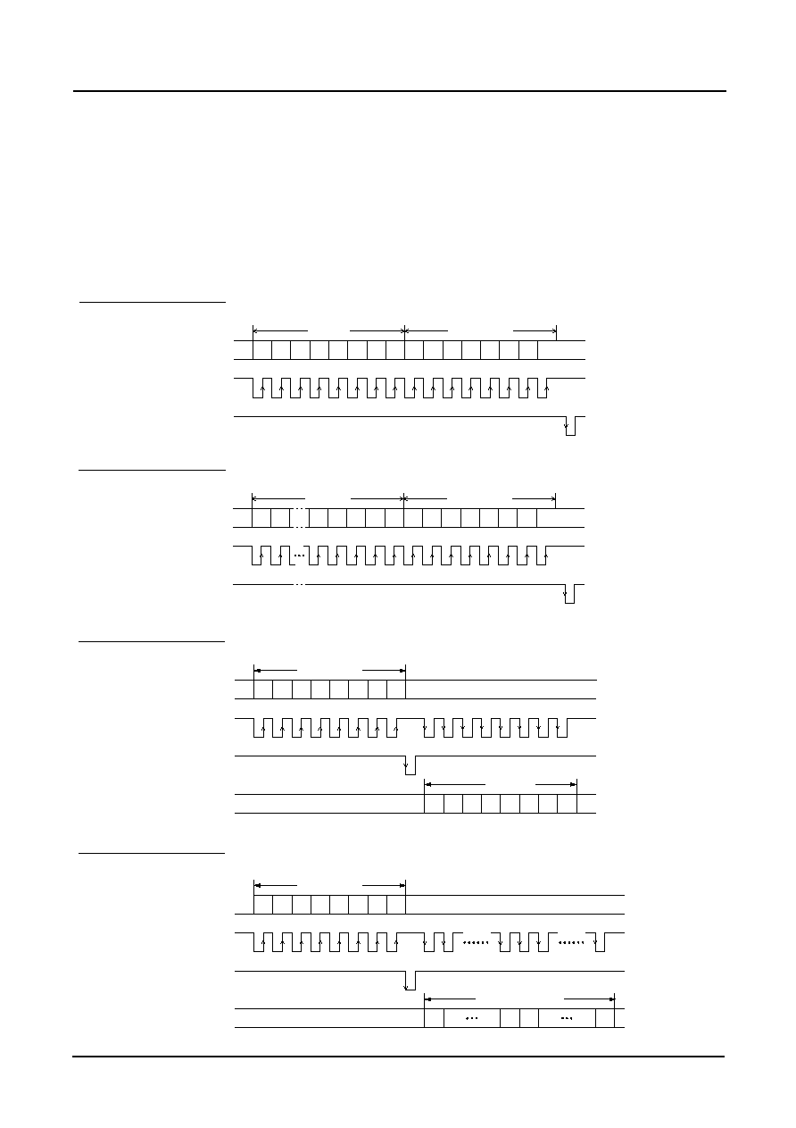
SM5904BF
YLRCK
16
LSB
MSB
LSB
MSB
R ch
LSB
YSCK
YSRDATA
L ch
1/(3fs )
16
9
ZLRCK
1
33
48
LSB
MSB
LSB
MSB
R ch
LSB
1/fs
ZSCK
ZSRDATA
L ch
24
Timing charts
Input timing (YSCK, YSRDATA, YLRCK)
Output timing (ZSCK, ZSRDATA, ZLRCK)
NIPPON PRECISION CIRCUITS-33
SM5904BF
,,,,,,,,,
,,,,,,,,,
,,,,,,,,,
,,,,,,,,,
,,,,,,,,,,,,,,
,,,,,,,,,,,,,,
,,,,,,,,,,,,,,
,,,,,,,,,,,,,,
,,,,,,,,,,,
,,,,,,,,,,,
,,,,,,,,,,,
,,,,,,,,,,,
,,,,,,,
,,,,,,,
,,,,,,,
,,,,,,,
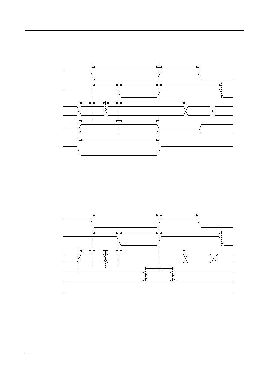
NCAS2
(DRAM2 SELECT)
A0 to A9
D0 to D3
(WRITE)
NRAS
NWE
t
RASH
t
RASL
t
t
CASL
CASH
t
CADS
t
RADH
t
t
RADS
CADH
t
CWDS
t
CWDH
t
WEL
t
RDC
DRAM write timing (NRAS, NCAS2, NWE, A0 to A9, D0 to D3)
Write timing (with double DRAM)
Use external DRAM.
DRAM read timing (NRAS, NCAS2, NWE, A0 to A9, D0 to D3)
Read timing (with double DRAM)
Use external DRAM.
,,,,,,,,,,,,,,,,,,,,,,,,
,,,,,,,,,,,,,,,,,,,,,,,,
,,,,,,,,,,,,,,,,,,,,,,,,
,,,,,,,,,,,,,,,,,,,,,,,,
,,,,,,,,
,,,,,,,,
,,,,,,,,
,,,,,,,,
,,,,,,,,,,,,
,,,,,,,,,,,,
,,,,,,,,,,,,
,,,,,,,,,,,,
,,,,,,,,,,,,,,,,,,,,,,,,,,,,,,,,,,
,,,,,,,,,,,,,,,,,,,,,,,,,,,,,,,,,,
,,,,,,,,,,,,,,,,,,,,,,,,,,,,,,,,,,
,,,,,,,,,,,,,,,,,,,,,,,,,,,,,,,,,,
,,,,,,,
,,,,,,,
,,,,,,,
,,,,,,,
NCAS2
(DRAM2 SELECT)
A0 to A9
NRAS
D0 to D3
(READ)
NWE
RASL
t
RASH
t
CASH
t
t
CASL
RCD
t
RADS
t
t
RADH
CADS
t
CADH
t
CRDS
t
CRDH
t
NIPPON PRECISION CIRCUITS-34
SM5904BF
Micro-
controller
DSP
Matsushita
MN662740
D/A
converter
SM5904
YMDATA
YMCLK
YMLD
ZSENSE
YBLKCK
YFLAG
YFCLK
YLRCK
YSCK
YSRDATA
ZLRCK
ZSCK
ZSRDATA
UC1 to UC4
NCAS2
CLK
NRESET
YDMUTE
DSP
SONY
CXD2517
SM5904
YMDATA
YMCLK
YMLD
ZSENSE
YBLKCK
YFCLK
YFLAG
YLRCK
YSCK
YSRDATA
NCAS2
CLK
NRESET
YDMUTE
SCOR
XROF
Micro-
controller
DIT
UC1 to UC4
DIT
A
D
ZSCK
ZLRCK
ZSRDATA
DRAM 2
A0 to A9
D0 to D3
RAS
WE
OE
CAS
DRAM 2
A0 to A9
D0 to D3
RAS
WE
OE
CAS
NRAS
NWE
A0 to A9
D0 to D3
NRAS
NWE
A0 to A9
D0 to D3
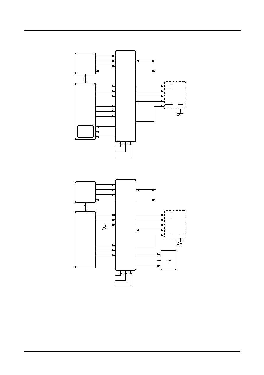
Connection example
note1
When 2 DRAMs are used, the DRAM OE pins should be tied LOW.
note 2 When CXD 2517 (Sony) is used
Set 85H of microcontroller command (option setting) as setting YFLAG take in;
D5: YFLAGS= 1
D4: YFCKP= 0

NIPPON PRECISION CIRCUITS-35
SM5904BF
NIPPON PRECISION CIRCUITS INC.
reserves the right to make changes to the products described in this data sheet in order to
improve the design or performance and to supply the best possible products. Nippon Precision Circuits Inc. assumes no responsibility for
the use of any circuits shown in this data sheet, conveys no license under any patent or other rights, and makes no claim that the circuits
are free from patent infringement. Applications for any devices shown in this data sheet are for illustration only and Nippon Precision
Circuits Inc. makes no claim or warranty that such applications will be suitable for the use specified without further testing or modifica-
tion. The products described in this data sheet are not intended to use for the apparatus which influence human lives due to the failure or
malfunction of the products. Customers are requested to comply with applicable laws and regulations in effect now and hereinafter, includ-
ing compliance with export controls on the distribution or dissemination of the products. Customers shall not export, directly or indirect-
ly, any products without first obtaining required licenses and approvals from appropriate government agencies.
NIPPON PRECISION CIRCUITS INC.
4-3, 2-chome Fukuzumi, Koto-ku
Tokyo, 135 -8430, JAPAN
Telephon: 03-3642-6661
Facsimile: 03-3642-6698
NC9820BE 1999.8
NIPPON PRECISION CIRCUITS INC.