WF5025 series
NIPPON PRECISION CIRCUITS INC.--1
Crystal Oscillator Module ICs
OVERVIEW
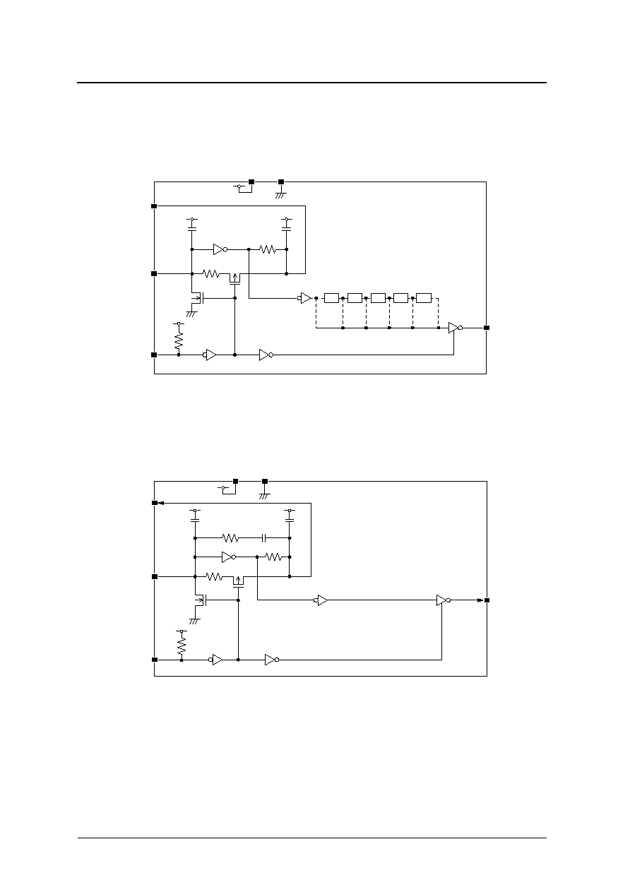
The WF5025 series are miniature crystal oscillator module ICs. They feature a damping resistor R
D
matched to
the crystal's characteristics to reduce crystal current. The pad layout is arranged for flip chip mounting, which
gives the pattern design more flexibility, even for mounting ultra-miniature crystal oscillators that provide
almost no space for wiring patterns. They support fundamental oscillation and 3rd overtone oscillation modes.
The WF5025 series can be used to correspond to wide range of applications.
FEATURES
I
Pad layout optimized for flip chip mounting
I
Miniature-crystal matched oscillator characteristics
I
Operating supply voltage range
∑ 2.5V operation: 2.25 to 2.75V
∑ 3.0V operation: 2.7 to 3.6V
I
Recommended operating frequency range
∑ For fundamental oscillator
- WF5025AL
◊
: 20MHz to 50MHz
- WF5025BL1: 20MHz to 100MHz
∑ For 3rd overtone oscillator
- WF5025ML
◊
: 70MHz to 133MHz
I
-
40 to 85
∞
C operating temperature range
I
Oscillator capacitor with excellent frequency char-
acteristics built-in
I
Oscillator circuit with damping resistor R
D
built-
in for reduced crystal current
I
Standby function
∑ High impedance in standby mode, oscillator
stops
I
Low standby current
∑ Power-saving pull-up resistor built-in
I
Oscillation detector function
I
Frequency divider built-in (WF5025AL
◊
)
∑ varies with version: f
O
, f
O
/2, f
O
/4, f
O
/8, f
O
/16,
f
O
/32
I
CMOS output duty level (1/2VDD)
I
50 ± 5% output duty @ 1/2VDD
I
30pF output load
I
Molybdenum-gate CMOS process
SERIES CONFIGURATION
Note. These versions in parentheses ( ) are under development. Please ask our Sales & Marketing section for further detail.
ORDERING INFORMATION
Version
Operating
supply voltage
[V]
Oscillation
mode
Recommended
operating frequency
range (fundamental
oscillation)
*1
[MHz]
*1. The recommended operating frequency is a yardstick value derived from the crystal used for NPC characteristics authentication. However, the oscil-
lator frequency band is not guaranteed. Specifically, the characteristics can vary greatly due to crystal characteristics and mounting conditions, so the
oscillation characteristics of components must be carefully evaluated.
Output
current
(V
DD
= 2.5V)
[mA]
Output
frequency
Output duty
level
Standby mode
Oscillator
stop
function
Output state
WF5025AL1
2.25 to 3.6
Fundamental
20 to 50
4
f
O
CMOS
Yes
Hi-Z
WF5025AL2
f
O
/2
WF5025AL3
f
O
/4
WF5025AL4
f
O
/8
WF5025AL5
f
O
/16
WF5025AL6
f
O
/32
WF5025BL1
*2
*2. The WF5025BL1 has a higher maximum operating frequency, hence the negative resistance is also larger than in the WF5025AL
◊
devices.
2.25 to 3.6
Fundamental
20 to 100
8
f
O
CMOS
Yes
Hi-Z
WF5025MLA
2.25 to 3.6
3rd overtone
70 to 80
8
f
O
CMOS
Yes
Hi-Z
(WF5025MLB)
80 to 100
WF5025MLC
90 to 133
Device
Package
WF5025
◊◊◊
≠3
Wafer form

WF5025 series
NIPPON PRECISION CIRCUITS INC.--2
PAD LAYOUT
(Unit:
µ
m)
PIN DESCRIPTION and PAD DIMENSIONS
Chip size: 0.75
◊
0.85mm
Chip thickness: 180 ± 20µm
PAD size: 90µm
Chip base: V
DD
level
Name
I/O
Description
Pad dimensions [µm]
X
Y
INHN
I
Output state control input. High impedance when LOW (oscillator stops).
Power-saving pull-up resistor built-in.
144.6
413.4
XT
I
Amplifier input
Crystal connection pins.
Crystal is connected between XT and XTN.
171.0
144.6
XTN
O
Amplifier output
579.0
144.6
VDD
≠
Supply voltage
618.2
438.6
Q
O
Output. Output frequency determined by internal circuit to one of f
O
, f
O
/2, f
O
/4, f
O
/8, f
O
/16,
f
O
/32. High impedance in standby mode
618.2
705.4
VSS
≠
Ground
131.8
718.2
Q
VDD
XTN
VSS
(0,0)
(750,850)
X
Y
HA5025
INHN
XT
NPC
WF5025 series
NIPPON PRECISION CIRCUITS INC.--4
SPECIFICATIONS
Absolute Maximum Ratings
V
SS
= 0V
Recommended Operating Conditions
V
SS
= 0V
Parameter
Symbol
Condition
Rating
Unit
Supply voltage range
V
DD
-
0.5 to +7.0
V
Input voltage range
V
IN
-
0.5 to V
DD
+ 0.5
V
Output voltage range
V
OUT
-
0.5 to V
DD
+ 0.5
V
Operating temperature range
T
opr
-
40 to +85
∞
C
Storage temperature range
T
STG
-
65 to +150
∞
C
Output current
I
OUT
20
mA
Parameter
Symbol
Condition
Rating
*1
*1. Values in parentheses ( ) are provisional only.
Unit
min
typ
max
Operating supply voltage
V
DD
WF5025AL
◊
CL
30pF
2.25
≠
3.6
V
WF5025BL1
CL
30pF
2.25
≠
3.6
V
WF5025MLA
f
80MHz, CL
30pF
2.25
≠
3.6
V
WF5025MLB
f
100MHz, CL
30pF
(2.25)
≠
(3.6)
V
WF5025MLC
f
100MHz, CL
30pF
2.25
≠
3.6
V
f
133MHz, CL
15pF
2.25
≠
3.6
V
Input voltage
V
IN
V
SS
≠
V
DD
V
Operating temperature
T
OPR
-
40
≠
+85
∞
C
Operating frequency
*2
*2. The operating frequency is a yardstick value derived from the crystal used for NPC characteristics authentication. However, the oscillator frequency
band is not guaranteed. Specifically, the characteristics can vary greatly due to crystal characteristics and mounting conditions, so the oscillation char-
acteristics of components must be carefully evaluated.
f
O
WF5025AL
◊
20
≠
50
MHz
WF5025BL1
*3
*3. When 2.5V operation, the ratings of switching characteristics are difference by the frequency or output load. Refer to "Switching Characteristics".
20
≠
100
MHz
WF5025MLA
70
≠
80
MHz
WF5025MLB
*3
(80)
≠
(100)
MHz
WF5025MLC
*3
90
≠
133
MHz
WF5025 series
NIPPON PRECISION CIRCUITS INC.--5
Electrical Characteristics
WF5025AL
◊
(2.5V operation)
V
DD
= 2.25 to 2.75V, V
SS
= 0V, Ta =
-
40 to +85
∞
C unless otherwise noted.
Parameter
Symbol
Condition
Rating
Unit
min
typ
max
HIGH-level output voltage
V
OH
Q: Measurement cct 1, V
DD
= 2.25V, I
OH
= 4mA
1.65
1.95
≠
V
LOW-level output voltage
V
OL
Q: Measurement cct 2, V
DD
= 2.25V, I
OL
= 4mA
≠
0.3
0.4
V
HIGH-level input voltage
V
IH
INHN
0.7V
DD
≠
≠
V
LOW-level input voltage
V
IL
INHN
≠
≠
0.3V
DD
V
Output leakage current
I
Z
Q: Measurement cct 2, INHN = LOW
V
OH
= V
DD
≠
≠
10
µA
V
OL
= V
SS
≠
≠
10
µA
Current consumption
I
DD2
Measurement cct 3, load cct 1,
INHN = open, C
L
= 30pF, f = 50MHz
WF5025AL1
≠
7
14
mA
WF5025AL2
≠
4.5
9
mA
WF5025AL3
≠
3.5
7
mA
WF5025AL4
≠
2.9
5.8
mA
WF5025AL5
≠
2.5
5
mA
WF5025AL6
≠
2.4
4.8
mA
Standby current
I
ST
Measurement cct 3, INHN = LOW
≠
≠
3
µA
INHN pull-up resistance
R
UP1
Measurement cct 4
2
6
12
M
R
UP2
20
100
200
k
Feedback resistance
R
f
Measurement cct 5
50
≠
150
k
Oscillator amplifier output
resistance
R
D
Design value. A monitor pattern on a wafer is tested.
340
400
460
Built-in capacitance
C
G
Design value. A monitor pattern on a wafer is tested.
6.8
8
9.2
pF
C
D
8.5
10
11.5
pF