 | –≠–ª–µ–∫—Ç—Ä–æ–Ω–Ω—ã–π –∫–æ–º–ø–æ–Ω–µ–Ω—Ç: 100315 | –°–∫–∞—á–∞—Ç—å:  PDF PDF  ZIP ZIP |
100315
Low-Skew Quad Clock Driver
General Description
The 100315 contains four low skew differential drivers, de-
signed for generation of multiple, minimum skew differential
clocks from a single differential input. This device also has
the capability to select a secondary single-ended clock
source for use in lower frequency system level testing. The
100315 is a 300 Series redesign of the 100115 clock driver.
Features
n
Low output to output skew (
50 ps)
n
Differential inputs and outputs
n
Secondary clock available for system level testing
n
2000V ESD protection
n
Voltage compensated operating range: -4.2V to -5.7V
n
Standard Microcircuit Drawing
(SMD) 5962-9469601
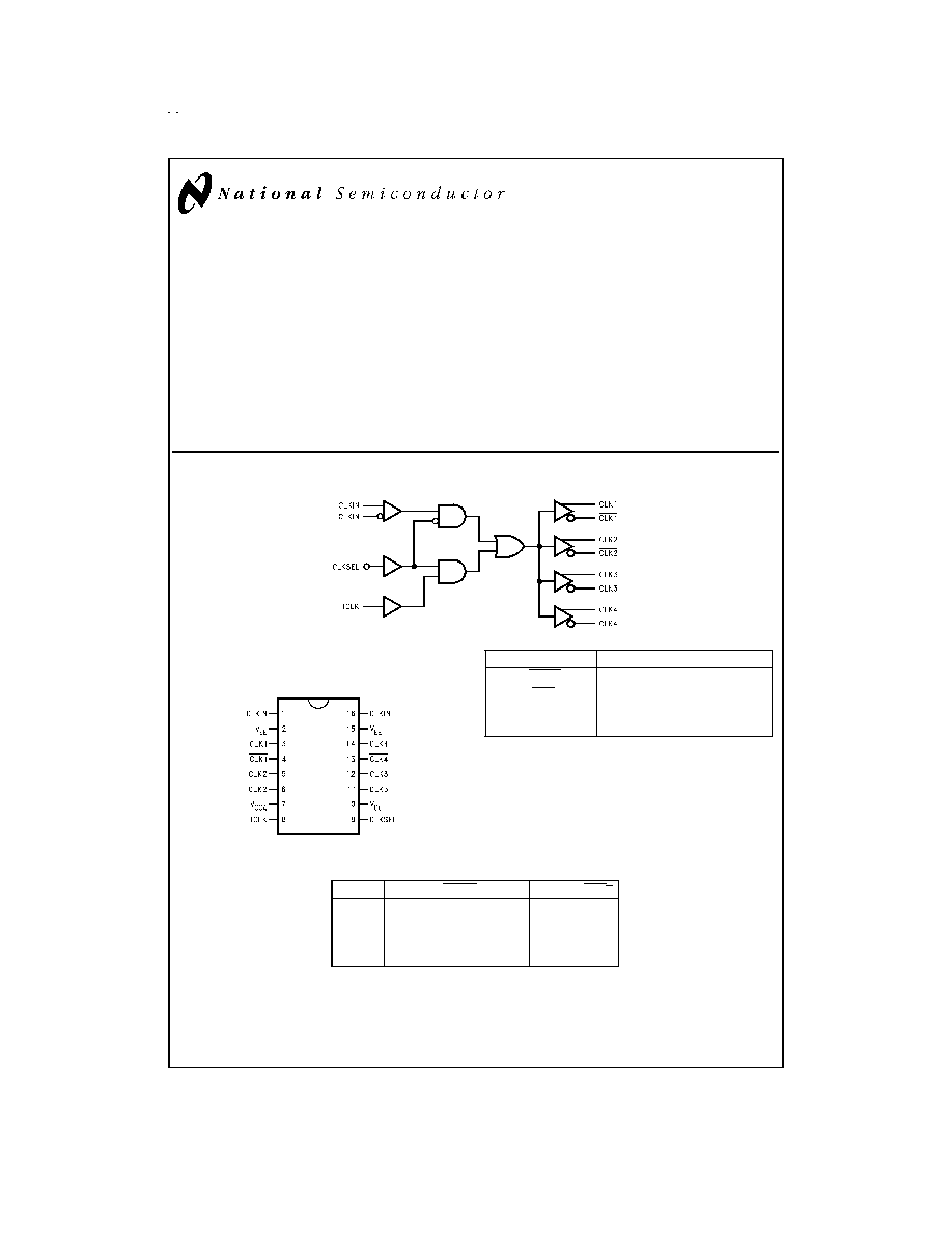
Logic Diagram
Connection Diagram
Pin Names
Description
CLKIN, CLKIN
Differential Clock Inputs
CLK
1≠4
, CLK
1≠4
Differential Clock Outputs
TCLK
Test Clock Input (Note 1)
CLKSEL
Clock Input Select (Note 1)
Note 1: TCLK and CLKSEL are single-ended inputs, with internal 50 k
pull-
down resistors.
Truth Table
CLKSEL
CLKIN
CLKIN
TCLK
CLK
N
CLK
N
L
L
H
X
L
H
L
H
L
X
H
L
H
X
X
L
L
H
H
X
X
H
H
L
L = Low Voltage Level
H = High Voltage Level
X = Don't Care
DS100319-1
Flatpak
DS100319-2
August 1998
100315
Low-Skew
Quad
Clock
Driver
© 1998 National Semiconductor Corporation
DS100319
www.national.com
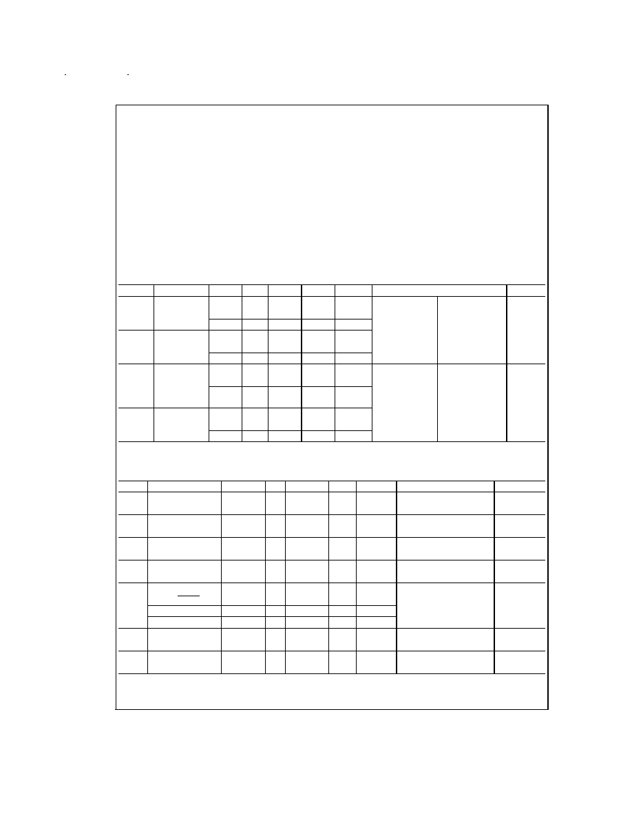
Absolute Maximum Ratings
(Note 2)
If Military/Aerospace specified devices are required,
please contact the National Semiconductor Sales Office/
Distributors for availability and specifications.
Above which the useful life may be impaired
Storage Temperature
-65∞C to +150∞C
Maximum Junction Temperature (T
J
)
Ceramic
+175∞C
Case Temperature under Bias (T
C
)
≠55∞C to +125∞C
V
EE
Pin Potential to Ground Pin
-7.0V to +0.5V
Input Voltage (DC)
V
CC
to +0.5V
Output Current (DC Output HIGH)
-50 mA
Operating Range (Note 2)
-5.7V to -4.2V
ESD (Note 3)
2000V
Recommended Operating
Conditions
Case Temperature (T
C
)
Military
-55∞C to +125∞C
Supply Voltage (V
EE
)
-5.7V to -4.2V
Note 2: Absolute maximum ratings are those values beyond which the de-
vice may be damaged or have its useful life impaired. Functional operation
under these conditions is not implied.
Note 3: ESD testing conforms to MIL-STD-883, Method 3015.
Military Version
DC Electrical Characteristics
V
EE
= -4.2V to -5.7V, V
CC
= V
CCA
= GND (Note 6)
Symbol
Parameter
Min
Typ
Max
Units
T
C
Conditions
Notes
V
OH
Output HIGH
-1025
-870
mV
0∞C to
V
IN
= V
IH(Max)
or V
IL(Min)
Loading with
50
to -2.0V
(Notes
4, 5, 6)
Voltage
+125∞C
-1085
-870
mV
-55∞C
V
OL
Output LOW
-1830
-1620
mV
0∞C to
Voltage
+125∞C
-1830
-1555
mV
-55∞C
V
OHC
Output HIGH
-1035
mV
0∞C to
V
IN
= V
IH(Min)
or V
IL(Max)
Loading with
50
to -2.0V
Voltage
+125∞C
-1085
mV
-55∞C
(Notes
4, 5, 6)
V
OLC
Output LOW
-1610
mV
0∞C to
Voltage
+125∞C
-1555
mV
-55∞C
DC Electrical Characteristics
V
EE
= -4.2V to -5.7V, V
CC
= V
CCA
= GND (Note 6)
Symbol
Parameter
Min
Typ
Max
Units
T
C
Conditions
Notes
V
DIFF
Input Voltage
150
mV
-55∞C to
Required for Full
(Notes 4, 5,
6)
Differential
+125∞C
Output Swing
V
CM
Common Mode
V
CC
- 2.0
V
CC
- 0.5
V
-55∞C to
(Notes 4, 5,
6)
Voltage
+125∞C
V
IH
Single-Ended
-1165
-870
mV
-55∞C to
Guaranteed HIGH Signal
(Notes 4, 5,
6, 7)
Input High Voltage
+125∞C
for All Inputs
V
IL
Single-Ended
-1830
-1475
mV
-55∞C to
Guaranteed LOW Signal
(Notes 4, 5,
6, 7)
Input Low Voltage
+125∞C
for All Inputs
I
IH
Input HIGH Current
150
µA
-55∞C to
V
IN
= V
IH(Max)
(Notes 4, 5,
6)
CLKIN, CLKIN
+125∞C
TCLK
450
µA
CLKSEL
380
µA
I
CBO
Input Leakage
-10
µA
-55∞C to
V
IN
= V
EE
(Notes 4, 5,
6)
Current
+125∞C
I
EE
Power Supply
-80
-25
mA
-55∞C to
(Notes 4, 5,
6)
Current, Normal
+125∞C
Note 4: F100K 300 Series cold temperature testing is performed by temperature soaking (to guarantee junction temperature equals -55∞C), then testing immediately
without allowing for the junction temperature to stabilize due to heat dissipation after power-up. This provides "cold start" specs which can be considered a worst case
condition at cold temperatures.
www.national.com
2
DC Electrical Characteristics
(Continued)
Note 5: Screen tested 100% on each device at -55∞C, +25∞C, and +125∞C, Subgroups 1, 2, 3, 7, and 8.
Note 6: Sample tested (Method 5005, Table I) on each manufactured lot at -55∞C, +25∞C, and +125∞C, Subgroups A1, 2, 3, 7, and 8.
Note 7: Guaranteed by applying specified input condition and testing V
OH
/V
OL
.
AC Electrical Characteristics
V
EE
= -4.2V to -5.7V, V
CC
= V
CCA
= GND
Symbol
Parameter
T
C
= -55∞C
T
C
= +25∞C
T
C
= +125∞C
Units
Conditions
Notes
Min
Max
Min
Max
Min
Max
t
PLH
Propagation Delay CLKIN,
0.58
0.88
0.63
0.88
0.72
1.02
ns
Figures 1, 2
(Notes 8, 9,
10)
t
PHL
CLKIN to CLK
(1≠4)
, CLK
(1≠4)
t
PLH
Propagation Delay, TCLK
0.30
1.60
0.30
1.50
0.40
1.70
ns
t
PHL
to CLK
(1≠4)
, CLK
(1≠4)
t
S G≠G
Skew Gate to Gate (Note 12)
120
100
120
ps
(Note 10)
t
TLH
Transition Time
0.30
0.90
0.25
0.85
0.20
0.85
ns
t
THL
20% to 80%, 80% to 20%
Note 8: F100K 300 Series cold temperature testing is performed by temperature soaking (to guarantee junction temperature equals -55∞C, then testing immediately
after power-up. This provides "cold start" specs which can be considered a worst case condition at cold temperatures.
Note 9: Screen tested 100% on each device at +25∞C temperature only, Subgroup A9.
Note 10: Sample tested (Method 5005, Table I) on each manufactured lot at +25∞C, Subgroup A9, and at +125∞C and -55∞C temperatures, Subgroups A10 and A11.
Note 11: Not tested at +25∞C, +125∞C and -55∞C temperature (design characterization data).
Note 12: Maximum output skew for any one device.
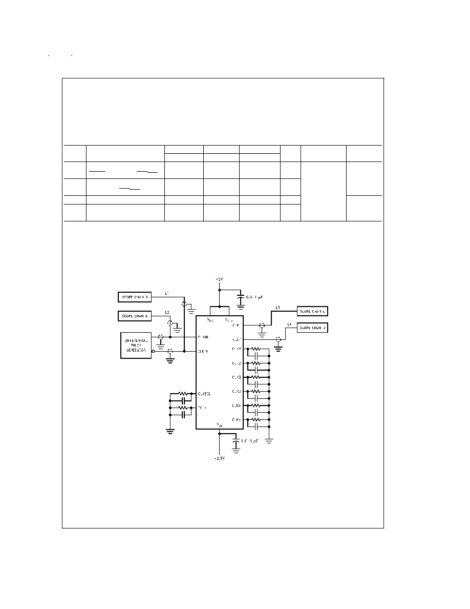
DS100319-3
Note 13: Shown for testing CLKIN to CLK1 in the differential mode.
Note 14: L1, L2, L3 and L4 = equal length 50
impedance lines.
Note 15: All unused inputs and outputs are loaded with 50
in parallel with
3 pF to GND.
Note 16: Scope should have 50
input terminator internally.
FIGURE 1. AC Test Circuit
www.national.com
3
AC Electrical Characteristics
(Continued)
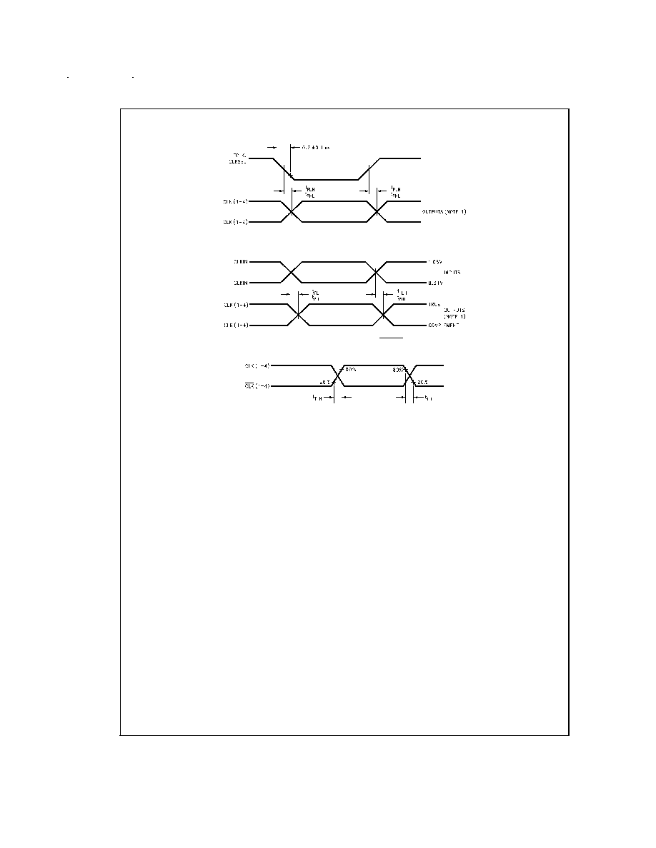
DS100319-4
FIGURE 2. Propagation Delay, TCLK, CLKSEL to Outputs
DS100319-5
FIGURE 3. Propagation Delay, CLKIN/CLKIN to Outputs
DS100319-6
Note 17: The output to output skew, which is defined as the difference in the propagation delays between each of the four outputs on any one 100115 shall not ex-
ceed 75 ps.
FIGURE 4. Transition Times
www.national.com
4

5