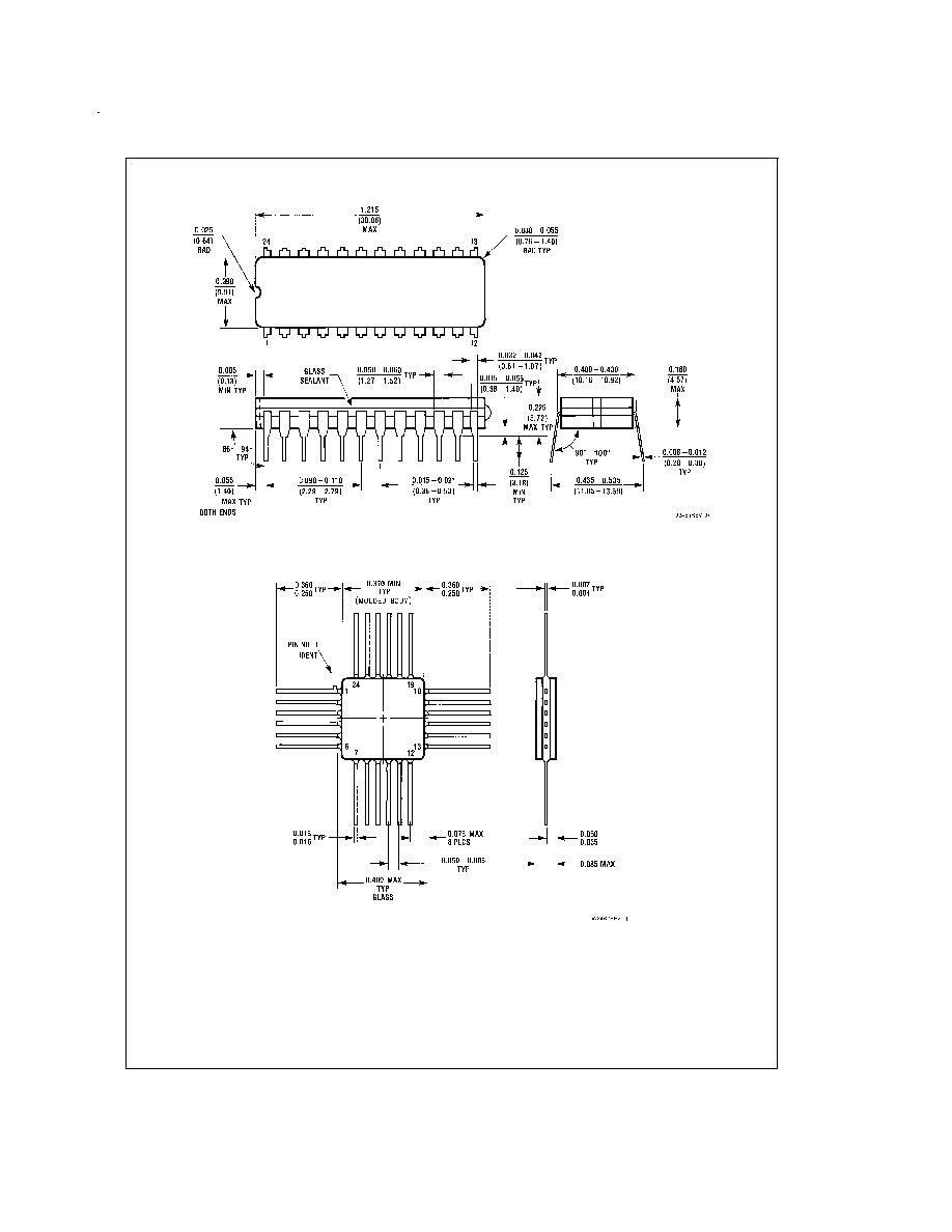
100322
Low Power 9-Bit Buffer
General Description
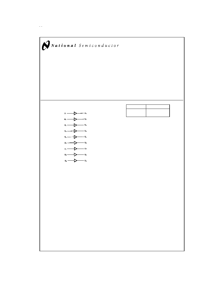
The 100322 is a monolithic 9-bit buffer. The device contains
nine non-inverting buffer gates with single input and output.
All inputs have 50 k
pull-down resistors and all outputs are
buffered.
Features
n
30% power reduction of the 100122
n
2000V ESD protection
n
Pin/function compatible with 100122
n
Voltage compensated operating range = -4.2V to -5.7V
n
Available to MIL-STD-883
Logic Symbol
Pin Names
Description
D
1
, D
9
Data Inputs
O
1
, O
9
Data Outputs
DS100308-1
August 1998
100322
Low
Power
9-Bit
Buffer
© 1998 National Semiconductor Corporation
DS100308
www.national.com

Absolute Maximum Ratings
(Note 1)
If Military/Aerospace specified devices are required,
please contact the National Semiconductor Sales Office/
Distributors for availability and specifications.
Above which the useful life may be impaired.
Storage Temperature (T
STG
)
-65∞C to +150∞C
Maximum Junction Temperature (T
J
)
Ceramic
+175∞C
V
EE
Pin Potential to Ground Pin
-7.0V to +0.5V
Input Voltage (DC)
V
EE
to +0.5V
Output Current (DC Output HIGH)
-50 mA
ESD (Note 2)
2000V
Recommended Operating
Conditions
Case Temperature (T
C
)
Military
-55∞C to +125∞C
Supply Voltage (V
EE
)
-5.7V to -4.2V
Note 1: Absolute maximum ratings are those values beyond which the de-
vice may be damaged or have its useful life impaired. Functional operation
under these conditions is not implied.
Note 2: ESD testing conforms to MIL-STD-883, Method 3015.
Military Version
DC Electrical Characteristics
V
EE
= -4.2V to -5.7V, V
CC
= V
CCA
= GND, T
C
= -55∞C to +125∞C
Symbol
Parameter
Min
Max
Units
T
C
Conditions
Notes
V
OH
Output HIGH Voltage -1025
-870
mV
0∞C to +125∞C
(Notes 3, 4, 5)
-1085
-870
mV
-55∞C
V
IN
=V
IH (Max)
Loading with
V
OL
Output LOW Voltage
-1830 -1620
mV
0∞C to +125∞C
or V
IL (Min)
50
to -2.0V
-1830 -1555
mV
-55∞C
V
OHC
Output HIGH Voltage -1035
mV
0∞C to +125∞C
(Notes 3, 4, 5)
-1085
mV
-55∞C
V
IN
=V
IH (Max)
Loading with
V
OLC
Output LOW Voltage
-1610
mV
0∞C to +125∞C
or V
IL (Min)
50
to -2.0V
-1555
mV
-55∞C
V
IH
Input HIGH Voltage
-1165
-870
mV
-55∞C to +125∞C
Guaranteed HIGH Signal
(Notes 3, 4, 5,
6)
for All Inputs
V
IL
Input HIGH Voltage
-1830 -1475
mV
-55∞C to +125∞C
Guaranteed LOW Signal
(Notes 3, 4, 5,
6)
for All Inputs
I
IL
Input LOW Current
0.50
µA
-55∞C to +125∞
V
EE
= -4.2V
(Notes 3, 4, 5)
V
IN
= V
IL (Min)
I
IH
Input HIGH Current
240
µA
0∞C to +125∞C
V
EE
= -5.7V
(Notes 3, 4, 5)
340
µA
-55∞C
V
IN
= V
IH (Max)
I
EE
Power Supply
Current
-70
-25
mA
-55∞C to +125∞C
Inputs Open
(Notes 3, 4, 5)
Note 3: F100K 300 Series cold temperature testing is performed by temperature soaking (to guarantee junction temperature equals -55∞C), then testing immediately
without allowing for the junction temperature to stabilize due to heat dissipation after power-up. This provides "cold start" specs which can be considered a worst case
condition at cold temperatures.
Note 4: Screen tested 100% on each device at -55∞C, +25∞C, and +125∞C, Subgroups 1, 2, 3, 7, and 8.
Note 5: Sample tested (Method 5005, Table I) on each manufactured lot at -55∞C, +25∞C, and +125∞C, Subgroups A1, 2, 3, 7, and 8.
Note 6: Guaranteed by applying specified input condition and testing V
OH
/V
OL
.
AC Electrical Characteristics
V
EE
= -4.2V to -5.7V, V
CC
= V
CCA
= GND
Symbol
Parameter
T
C
= -55∞C
T
C
= +25∞C
T
C
= +125∞C
Units
Conditions
Notes
Min
Max
Min
Max
Min
Max
t
PLH
Propagation Delay
0.30
1.80
0.40
1.60
0.40
1.80
ns
(Notes 7, 8,
9, 11)
t
PHL
Data to Output
Figures 1, 2
t
TLH
Transition Time
0.30
1.20
0.30
1.20
0.30
1.20
ns
(Note 10)
t
THL
20% to 80%, 80% to
20%
Note 7: F100K 300 Series cold temperature testing is performed by temperature soaking (to guarantee junction temperature equals -55∞C), then testing immediately
after power-up. This provides "cold start" specs which can be considered a worst case condition at cold temperatures.
Note 8: Screen tested 100% on each device at +25∞C, only Subgroup A9.
Note 9: Sample tested (Method 5005, Table I) on each manufactured lot at +25∞C, Subgroup A9, and at +125∞C and -55∞C temperatures, Subgroups A10 and A11.
www.national.com
3
AC Electrical Characteristics
(Continued)
Note 10: Not tested at +25∞C, +125∞C, and -55∞C temperature (design characterization data).
Note 11: The propagation delay specified is for single output switching. Delays may vary up to 200 ps with multiple outputs switching.
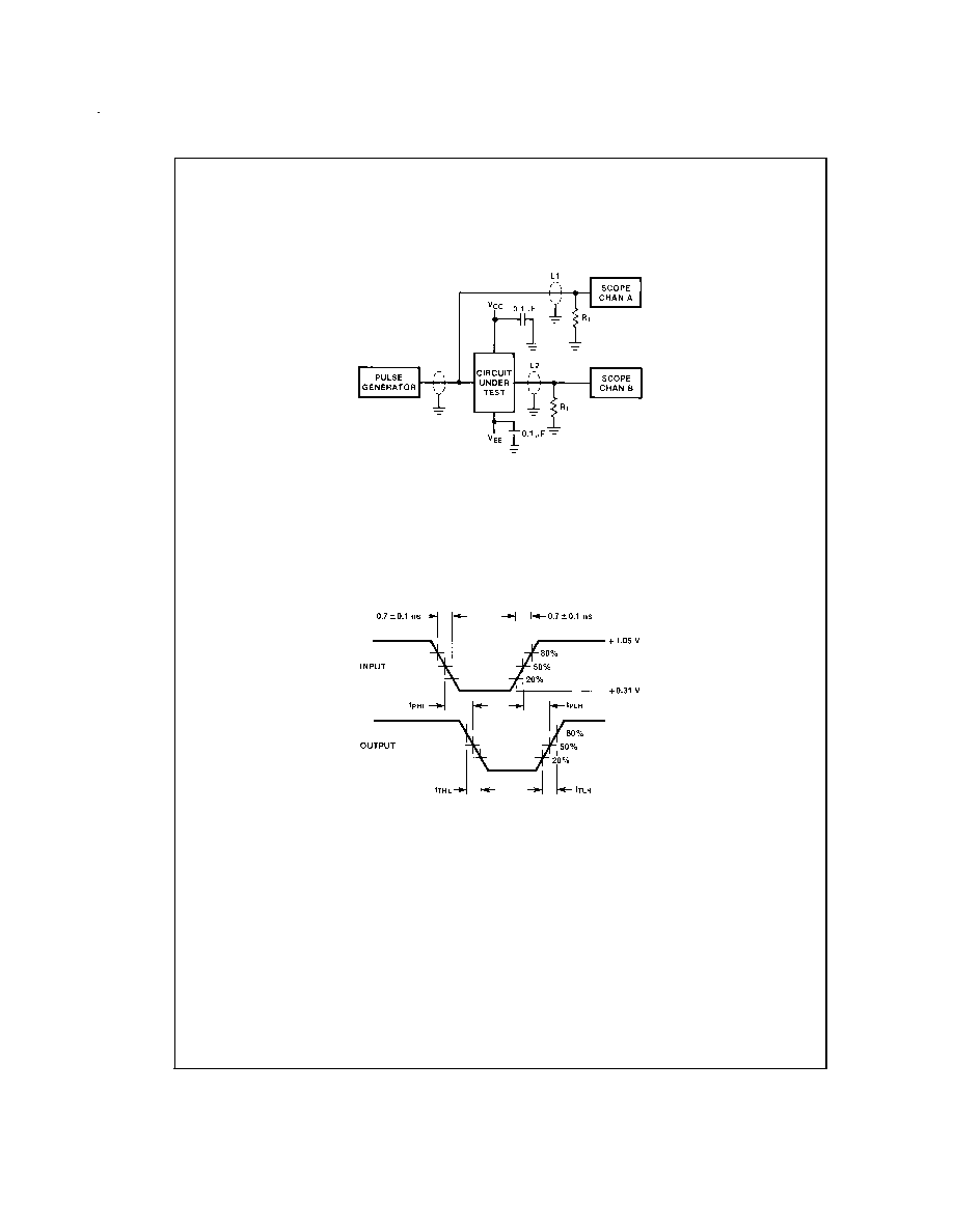
Test Circuit
Switching Waveforms
DS100308-5
Notes:
V
CC
, V
CCA
= +2V, V
EE
= -2.5V
L1 and L2 = equal length 50
impedance lines
R
T
= 50
terminator internal to scope
Decoupling 0.1 µF from GND to V
CC
and V
EE
All unused outputs are loaded with 50
to GND
C
L
= Fixture and stray capacitance
3 pF
FIGURE 1. AC Test Circuit
DS100308-6
FIGURE 2. Propagation Delay and Transition Times
www.national.com
4