 | –≠–ª–µ–∫—Ç—Ä–æ–Ω–Ω—ã–π –∫–æ–º–ø–æ–Ω–µ–Ω—Ç: 100329 | –°–∫–∞—á–∞—Ç—å:  PDF PDF  ZIP ZIP |

100329
Low Power Octal ECL/TTL Bidirectional Translator with
Register
General Description
The 100329 is an octal registered bidirectional translator de-
signed to convert TTL logic levels to 100K ECL logic levels
and vice versa. The direction of the translation is determined
by the DIR input. A LOW on the output enable input (OE)
holds the ECL outputs in a cut-off state and the TTL outputs
at a high impedance level. The outputs change synchro-
nously with the rising edge of the clock input (CP) even
though only one output is enabled at the time.
The cut-off state is designed to be more negative than a nor-
mal ECL LOW level. This allows the output emitter-followers
to turn off when the termination supply is -2.0V, presenting a
high impedance to the data bus. This high impedance re-
duces the termination power and prevents loss of low state
noise margin when several loads share the bus.
The 100329 is designed with FAST
Æ
TTL output buffers, fea-
turing optimal DC drive and capable of quickly charging and
discharging highly capacitive loads. All inputs have 50 k
pull-down resistors.
Features
n
Bidirectional translation
n
ECL high impedance outputs
n
Registered outputs
n
FAST TTL outputs
n
TRI-STATE
Æ
outputs
n
Voltage compensated operating range = -4.2V to -5.7V
n
Standard Microcircuit Drawing
(SMD) 5962-9206601
Connection Diagrams
TRI-STATE
Æ
is a registered trademark of National Semiconductor Corporation.
FAST
Æ
is a registered trademark of Fairchild Semiconductor.
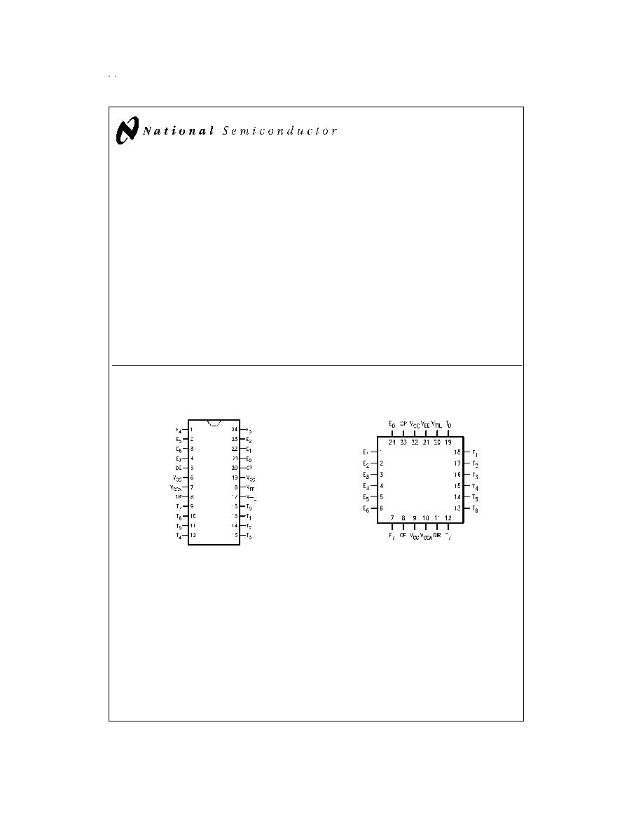
24-Pin DIP
DS100306-2
24-Pin Quad Cerpack
DS100306-4
September 1999
100329
Low
Power
Octal
ECL/TTL
Bidirectional
T
ranslator
with
Register
© 1999 National Semiconductor Corporation
DS100306
www.national.com

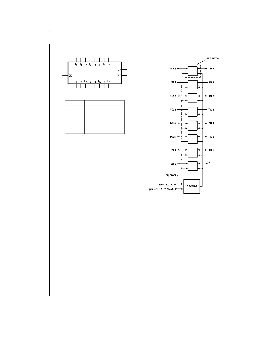
Logic Symbol
Pin Descriptions
Pin Names
Description
E
0
≠E
7
ECL Data I/O
T
0
≠T
7
TTL Data I/O
OE
Output Enable Input
CP
Clock Pulse Input
(Active Rising Edge)
DIR
Direction Control Input
All pins function at 100K ECL levels except for T
0
≠T
7
.
Functional Diagram
DS100306-1
DS100306-5
Note: DIR and OE use ECL logic levels
www.national.com
2

Detail
OE
DIR
CP
ECL
TTL
Notes
Port
Port
L
L
X
Input
Z
1, 3
L
H
X
LOW
Input
2, 3
(Cut-Off)
H
L
N
L
L
1
H
L
N
H
H
1
H
L
L
X
NC
1, 3
H
H
N
L
L
2
H
H
N
H
H
2
H
H
L
NC
X
2, 3
H = HIGH Voltage Level
L = LOW Voltage Level
X = Don't Care
Z = High Impedance
N
= LOW-to-HIGH Clock Transition
NC = No Change
Note 1: ECL input to TTL output mode.
Note 2: TTL input to ECL output mode.
Note 3: Retains data present before CP.
DS100306-6
www.national.com
3

Absolute Maximum Ratings
(Note 4)
If Military/Aerospace specified devices are required,
please contact the National Semiconductor Sales Office/
Distributors for availability and specifications.
Storage Temperature (T
STG
)
-65∞C to +150∞C
Maximum Junction Temperature (T
j
)
Ceramic
+175∞C
V
EE
Pin Potential to
Ground Pin
-7.0V to +0.5V
V
TTL
Pin Potential to
Ground Pin
-0.5V to +6.0V
ECL Input Voltage (DC)
V
EE
to +0.5V
ECL Output Current
(DC Output HIGH)
-50 mA
TTL Input Voltage (Note 6)
-0.5V to +6.0V
TTL Input Current (Note 6)
-30 mA to +5.0 mA
Voltage Applied to Output in HIGH State
TRI-STATE Output
-0.5V to +5.5V
Current Applied to TTL
Output in LOW State (Max)
Twice the Rated I
OL
(mA)
ESD (Note 5)
2000V
Recommended Operating
Conditions
Case Temperature (T
C
)
Military
≠55∞C to +125∞C
ECL Supply Voltage (V
EE
)
-5.7V to -4.2V
TTL Supply Voltage (V
TTL
)
+4.5V to +5.5V
Note 4: Absolute maximum ratings are those values beyond which the de-
vice may be damaged or have its useful life impaired. Functional operation
under these conditions is not implied.
Note 5: ESD testing conforms to MIL-STD-883, Method 3015.
Note 6: Either voltage limit or current limit is sufficient to protect inputs.
Military Version
TTL-to-ECL DC Electrical Characteristics
V
EE
= -4.2V to -5.7V, V
CC
= V
CCA
= GND, T
C
= -55∞C to +125∞C, V
TTL
= +4.5V to +5.5V
Symbol
Parameter
Min
Max
Units
T
C
Conditions
Notes
V
OH
Output HIGH Voltage
-1025
-870
mV
0∞C to
Loading with
50
to -2.0V
(Notes 7, 8,
9)
+125∞C
-1085
-870
mV
-55∞C
V
IN
= V
IH
(Max)
V
OL
Output LOW Voltage
-1830
-1620
mV
0∞C to
or V
IL
(Min)
+125∞C
-1830
-1555
mV
-55∞C
Cutoff Voltage
-1950
mV
0∞C to
+125∞C
OE or DIR Low
-1850
mV
-55∞C
V
OHC
Output HIGH Voltage
-1035
mV
0∞C to
(Notes 7, 8,
9)
+125∞C
-1085
mV
-55∞C
V
IN
= V
IH
(Min)
Loading with
V
OLC
Output LOW Voltage
-1610
mV
0∞C to
or V
IL
(Max)
50
0 to -2.0V
+125∞C
-1555
mV
-55∞C
V
IH
Input HIGH Voltage
2.0
V
-55∞C to
Over V
TTL
, V
EE
, T
C
Range
(Notes 7, 8,
9, 10)
+125∞C
V
IL
Input LOW Voltage
0.8
V
-55∞C to
Over V
TTL
, V
EE
, T
C
Range
(Notes 7, 8,
9, 10)
+125∞C
I
IH
Input HIGH Current
70
µA
-55∞C to
V
IN
= +2.7V
(Notes 7, 8,
9)
125∞C
Breakdown Test
1.0
mA
-55∞C to
V
IN
= +5.5V
+125∞C
I
IL
Input LOW Current
-1.0
mA
-55∞C to
V
IN
= +0.5V
(Notes 7, 8,
9)
+125∞C
V
FCD
Input Clamp
-1.2
V
-55∞C to
I
IN
= -18 mA
(Notes 7, 8,
9)
Diode Voltage
+125∞ C
I
EE
V
EE
Supply Current
-55∞C to
OE and DIR High
(Notes 7, 8,
9)
Inputs Open
-206
-70
mA
+125∞C
V
EE
= -4.2V to -5.7V
www.national.com
4

Military Version
ECL-to-TTL DC Electrical Characteristics
V
EE
= -4.2V to -5.7V, V
CC
= V
CCA
= GND, T
C
= -55∞C to +125∞C, C
L
= 50 pF, V
TTL
= +4.5V to + 5.5V
Symbol
Parameter
Min
Max Units
T
C
Conditions
Notes
V
OH
Output HIGH Voltage
2.5
mV
0∞C to +125∞C
I
OH
= -1 mA, V
TTL
= 4.50V
(Notes 7, 8, 9)
2.4
-55∞C
V
OL
Output LOW Voltage
0.5
mV
-55∞C
I
OL
= 24 mA, V
TTL
= 4.50V
+125∞C
V
IH
Input HIGH Voltage
-1165
-870
mV
-55∞C
Guaranteed HIGH Signal
(Notes 7, 8, 9, 10)
+125∞C
for All Inputs
V
IL
Input LOW Voltage
-1830 -1475
mV
-55∞C to
Guaranteed LOW Signal
(Notes 7, 8, 9, 10)
+125∞C
for All Inputs
I
IH
Input HIGH Current
350
µA
0∞C to
V
EE
= -5.7V
(Notes 7, 8, 9)
500
+125∞C
V
IN
= V
IH
(Max)
I
IL
Input LOW Current
0.50
µA
-55∞C to
V
EE
= -4.2V
(Notes 7, 8, 9)
+125∞C
V
IN
= V
IL
(Min)
I
OZHT
TRI-STATE Current
70
µA
-55∞C to
V
OUT
= +2.7V
(Notes 7, 8, 9)
Output High
+125∞C
I
OZLT
TRI-STATE Current
-1.0
mA
-55∞C to
V
OUT
= +0.5V
(Notes 7, 8, 9)
Output Low
+125∞C
I
OS
Output Short-Circuit
-60
-150
mA
-55∞C to
V
OUT
= 0.0V, V
TTL
= +5.5V
(Notes 7, 8, 9)
CURRENT
+125∞C
I
TTL
V
TTL
Supply Current
70
mA
-55∞C to
TTL Outputs Low
(Notes 7, 8, 9)
47
mA
+125∞C
TTL Output High
70
mA
TTL Output in TRI-STATE
Note 7: F100K 300 Series cold temperature testing is performed by temperature soaking (to guarantee junction temperature equals -55∞C), then testing immediately
without allowing for the junction temperature to stabilize due to heat dissipation after power-up. This provides "cold start" specs which can be considered a worst case
condition at cold temperatures.
Note 8: Screen tested 100% on each device at -55∞C, +25∞C, and +125∞C, Subgroups, 1, 2 3, 7, and 8.
Note 9: Sample tested (Method 5005, Table I) on each manufactured lot at -55∞C, +25∞C, and +125∞C, Subgroups A1, 2, 3, 7, and 8.
Note 10: Guaranteed by applying specified input condition and testing V
OH
/V
OL
.
Military Version
TTL-to-ECL AC Electrical Characteristics
V
EE
= -4.2V to -5.7V, V
TTL
= +4.5V to +5.5V, V
CC
= V
CCA
= GND
Symbol
Parameter
T
C
= -55∞C
T
C
= 25∞C
T
C
=
+125∞C
Units
Conditions
Notes
Min
Max
Min
Max
Min
Max
t
PLH
CP to E
n
1.3
3.8
1.6
3.7
1.9
4.3
ns
Figures 1, 2
(Notes 11,
12, 13)
t
PHL
ns
t
PZH
OE to E
n
1.0
4.3
1.5
4.4
1.7
9.0
ns
Figures 1, 2
(Notes 11,
12, 13)
(Cutoff to HIGH)
t
PHZ
OE to E
n
1.5
5.0
1.6
4.5
1.6
5.0
ns
Figures 1, 2
(HIGH to Cutoff)
t
PHZ
DIR to E
n
1.6
4.7
1.6
4.3
1.7
4.7
ns
Figures 1, 2
(HIGH to Cutoff)
t
set
T
n
to CP
2.5
2.0
2.5
ns
Figures 1, 2
(Note 14)
t
hold
T
n
to CP
2.5
2.0
2.5
ns
Figures 1, 2
t
pw
(H)
Pulse Width CP
2.5
2.0
2.5
ns
Figures 1, 2
(Note 14)
t
TLH
Transition Time
0.4
2.3
0.5
2.1
0.4
2.4
ns
Figures 1, 2
(Note 14)
t
THL
20% to 80%, 80% to 20%
f
MAX
CP
250
250
250
MHz
www.national.com
5


