 | –≠–Ľ–Ķ–ļ—ā—Ä–ĺ–Ĺ–Ĺ—č–Ļ –ļ–ĺ–ľ–Ņ–ĺ–Ĺ–Ķ–Ĺ—ā: 100336D | –°–ļ–į—á–į—ā—Ć:  PDF PDF  ZIP ZIP |

100336
Low Power 4-Stage Counter/Shift Register
General Description
The 100336 operates as either a modulo-16 up/down
counter or as a 4-bit bidirectional shift register. Three Select
(S
n
) inputs determine the mode of operation, as shown in the
Function Select table. Two Count Enable (CEP, CET) inputs
are provided for ease of cascading in multistage counters.
One Count Enable (CET) input also doubles as a Serial Data
(D
0
) input for shift-up operation. For shift-down operation, D
3
is the Serial Data input. In counting operations the Terminal
Count (TC) output goes LOW when the counter reaches 15
in the count/up mode or 0 (zero) in the count/down mode. In
the shift modes, the TC output repeats the Q
3
output. The
dual nature of this TC/Q
3
output and the D
0
/CET input
means that one interconnection from one stage to the next
higher stage serves as the link for multistage counting or
shift-up operation. The individual Preset (P
n
) inputs are used
to enter data in parallel or to preset the counter in program-
mable counter applications. A HIGH signal on the Master Re-
set (MR) input overrides all other inputs and asynchronously
clears the flip-flops. In addition, a synchronous clear is pro-
vided, as well as a complement function which synchro-
nously inverts the contents of the flip-flops. All inputs have 50
k
pull-down resistors.
Features
n
40% power reduction of the 100136
n
2000V ESD protection
n
Pin/function compatible with 100136
n
Voltage compensated operating range = -4.2V to -5.7V
n
Standard Microcircuit Drawing
(SMD) 5962-9230601
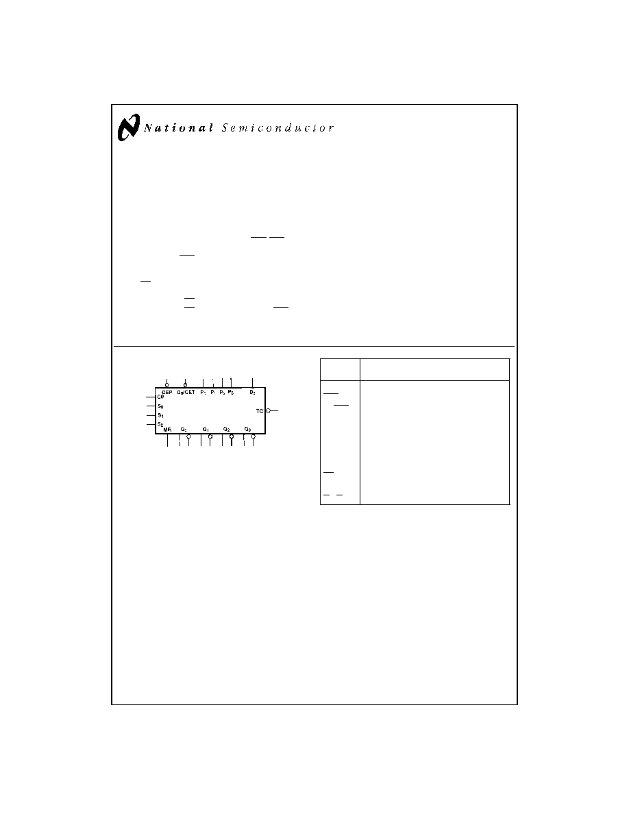
Logic Symbol
Pin
Names
Description
CP
Clock Pulse Input
CEP
Count Enable Parallel Input (Active LOW)
D
0
/CET
Serial Data Input/Count Enable
Trickle Input (Active LOW)
S
0
≠S
2
Select Inputs
MR
Master Reset Input
P
0
≠P
3
Preset Inputs
D
3
Serial Data Input
TC
Terminal Count Output
Q
0
≠Q
3
Data Outputs
Q
0
≠Q
3
Complementary Data Outputs
DS100307-1
August 1998
100336
Low
Power
4-Stage
Counter/Shift
Register
© 1998 National Semiconductor Corporation
DS100307
www.national.com

Connection Diagrams
24-Pin DIP
DS100307-2
24-Pin Quad Cerpak
DS100307-3
www.national.com
2

Logic Diagram
DS100307-5
3
www.national.com

Function Select Table
S
2
S
1
S
0
Function
L
L
L
Parallel Load
L
L
H
Complement
L
H
L
Shift Left
L
H
H
Shift Right
H
L
L
Count Down
H
L
H
Clear
H
H
L
Count Up
H
H
H
Hold
Truth Table
Q
0
= LSB
Inputs
Outputs
MR
S
2
S
1
S
0
CEP
D
0
/CET
D
3
CP
Q
3
Q
2
Q
1
Q
0
TC
Mode
L
L
L
L
X
X
X
N
P
3
P
2
P
1
P
0
L
Preset (Parallel Load)
L
L
L
H
X
X
X
N
Q
3
Q
2
Q
1
Q
0
L
Invert
L
L
H
L
X
X
X
N
D
3
Q
3
Q
2
Q
1
D
3
Shift to LSB
L
L
H
H
X
X
X
N
Q
2
Q
1
Q
0
D
0
Q
3
(Note 1)
Shift to MSB
L
H
L
L
L
L
X
N
(Q
0≠3
) minus 1
1
Count Down
L
H
L
L
H
L
X
X
Q
3
Q
2
Q
1
Q
0
1
Count Down with CEP not active
L
H
L
L
X
H
X
X
Q
3
Q
2
Q
1
Q
0
H
Count Down with CET not active
L
H
L
H
X
X
X
N
L
L
L
L
H
Clear
L
H
H
L
L
L
X
N
(Q
0≠3
) plus 1
2
Count Up
L
H
H
L
H
L
X
X
Q
3
Q
2
Q
1
Q
0
2
Count Up with CEP not active
L
H
H
L
X
H
X
X
Q
3
Q
2
Q
1
Q
0
H
Count Up with CET not active
L
H
H
H
X
X
X
X
Q
3
Q
2
Q
1
Q
0
H
Hold
H
L
L
L
X
X
X
X
L
L
L
L
L
H
L
L
H
X
X
X
X
L
L
L
L
L
H
L
H
L
X
X
X
X
L
L
L
L
L
H
L
H
H
X
X
X
X
L
L
L
L
L
Asynchronous
H
H
L
L
X
L
X
X
L
L
L
L
L
Master Reset
H
H
L
L
X
H
X
X
L
L
L
L
H
H
H
L
H
X
X
X
X
L
L
L
L
H
H
H
H
L
X
X
X
X
L
L
L
L
H
H
H
H
H
X
X
X
X
L
L
L
L
H
1 =
L if Q
0
≠Q
3
= LLLL
H if Q
0
≠Q
3
LLLL
2 = L if Q
0
≠Q
3
= HHHH
H if Q
0
≠Q
3
HHHH
H = HIGH Voltage Level
L = LOW Voltage Level
X = Don't Care
N
= LOW-to-HIGH Transition
Note 1: Before the clock, TC is Q
3
After the clock, TC is Q
2
www.national.com
4

Absolute Maximum Ratings
(Note 2)
If Military/Aerospace specified devices are required,
please contact the National Semiconductor Sales Office/
Distributors for availability and specifications.
Storage Temperature (T
STG
)
-65įC to +150įC
Maximum Junction Temperature (T
J
)
Ceramic
+175įC
V
EE
Pin Potential to Ground Pin
-7.0V to +0.5V
Input Voltage (DC)
V
EE
to +0.5V
Output Current (DC Output HIGH)
-50 mA
ESD (Note 3)
2000V
Recommended Operating
Conditions
Case Temperature (T
C
)
Military
-55įC to +125įC
Supply Voltage (V
EE
)
-5.7V to -4.2V
Note 2: Absolute maximum ratings are those values beyond which the de-
vice may be damaged or have its useful life impaired. Functional operation
under these conditions is not implied.
Note 3: ESD testing conforms to MIL-STD-883, Method 3015.
Military Version
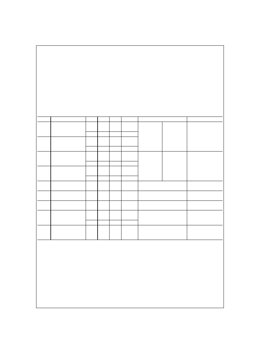
DC Electrical Characteristics
V
EE
= -4.2V to -5.7V, V
CC
= V
CCA
= GND, T
C
= -55įC to +125įC
Symbol
Parameter
Min
Max
Units
T
C
Conditions
Notes
V
OH
Output HIGH Voltage
-1025
-870
mV
0įC to
+125įC
V
IN
= V
IH (Max)
Loading with
-1085
-870
mV
-55įC
or V
IL (Min)
50
to -2.0V
(Notes 4, 5, 6)
V
OL
Output LOW Voltage
-1830
-1620
mV
0įC to
+125įC
-1830
-1555
mV
-55įC
V
OHC
Output HIGH Voltage
-1035
mV
0įC to
+125įC
V
IN
= V
IH (Min)
Loading with
-1085
mV
-55įC
or V
IL (Max)
50
to -2.0V
(Notes 4, 5, 6)
V
OLC
Output LOW Voltage
-1610
mV
0įC to
+125įC
-1555
mV
-55įC
V
IH
Input HIGH Voltage
-1165
-870
mV
-55įC to
Guaranteed HIGH Signal
(Notes 4, 5, 6, 7)
+125įC
for All Inputs
V
IL
Input LOW Voltage
-1830
-1475
mV
-55įC to
Guaranteed LOW Signal
(Notes 4, 5, 6, 7)
+125įC
for All Inputs
I
IL
Input LOW Current
0.50
ĶA
-55įC to
V
EE
= -4.2V
(Notes 4, 5, 6)
+125įC
V
IN
= V
IL (Min)
I
IH
Input HIGH Current
240
ĶA
0įC to
V
EE
= -5.7V
+125įC
V
IN
= V
IH(Max)
(Notes 4, 5, 6)
340
ĶA
-55įC
I
EE
Power Supply Current
-55įC
Inputs Open
-185
-70
mA
to
V
EE
= -4.2V to -4.8V
(Notes 4, 5, 6)
-195
-70
+125įC
V
EE
= -4.2V to -5.7V
Note 4: F100K 300 Series cold temperature testing is performed by temperature soaking (to guarantee junction temperature equals -55įC), then testing immediately
without allowing for the junction temperature to stablize due to heat dissipation after power-up. This provides "cold start" specs which can be considered a worst case
condition at cold temperatures.
Note 5: Screen tested 100% on each device at -55įC, +25įC, and +125įC, Subgroups 1, 2, 3, 7, and 8.
Note 6: Sample tested (Method 5005, Table I) on each manufactured lot at -55įC, +25įC, +125įC, Subgroups A1, 2, 3, 7, and 8.
Note 7: Guaranteed by applying specified input conditon and testing V
OH
/V
OL
.
5
www.national.com


