 | –≠–Ľ–Ķ–ļ—ā—Ä–ĺ–Ĺ–Ĺ—č–Ļ –ļ–ĺ–ľ–Ņ–ĺ–Ĺ–Ķ–Ĺ—ā: 100370D | –°–ļ–į—á–į—ā—Ć:  PDF PDF  ZIP ZIP |
100370
Low Power Universal Demultiplexer/Decoder
General Description
The 100370 universal demultiplexer/decoder functions as ei-
ther a dual 1-of-4 decoder or as a single 1-of-8 decoder, de-
pending on the signal applied to the Mode Control (M) input.
In the dual mode, each half has a pair of active-LOW Enable
(E) inputs. Pin assignments for the E inputs are such that in
the 1-of-8 mode they can easily be tied together in pairs to
provide two active-LOW enables (E
1a
to E
1b
, E
2a
to E
2b
).
Signals applied to auxiliary inputs H
a
, H
b
and H
c
determine
whether the outputs are active HIGH or active LOW. In the
dual 1-of-4 mode the Address inputs are A
0a
, A
1a
and A
0b
,
A
1b
with A
2a
unused (i.e., left open, tied to V
EE
or with LOW
signal applied). In the 1-of-8 mode, the Address inputs are
A
0a
, A
1a
, A
2a
with A
0b
and A
1b
LOW or open. All inputs have
50 k
pulldown resistors.
Features
n
35% power reduction of the 100170
n
2000V ESD protection
n
Pin/function compatible with 100170
n
Voltage compensated operating range = -4.2V to -5.7V
Logic Symbols
Pin Names
Description
A
na
, A
nb
Address Inputs
E
na
, E
nb
Enable Inputs
M
Mode Control Input
H
a
Z
0
≠Z
3
(Z
0a
≠Z
3a
)
Polarity Select Input
H
b
Z
4
≠Z
7
(Z
0b
≠Z
3b
)
Polarity Select Input
H
c
Common Polarity
Select Input
Z
0
≠Z
7
Single 1-of-8
Data Outputs
Z
na
, Z
nb
Dual 1-of-4
Data Outputs
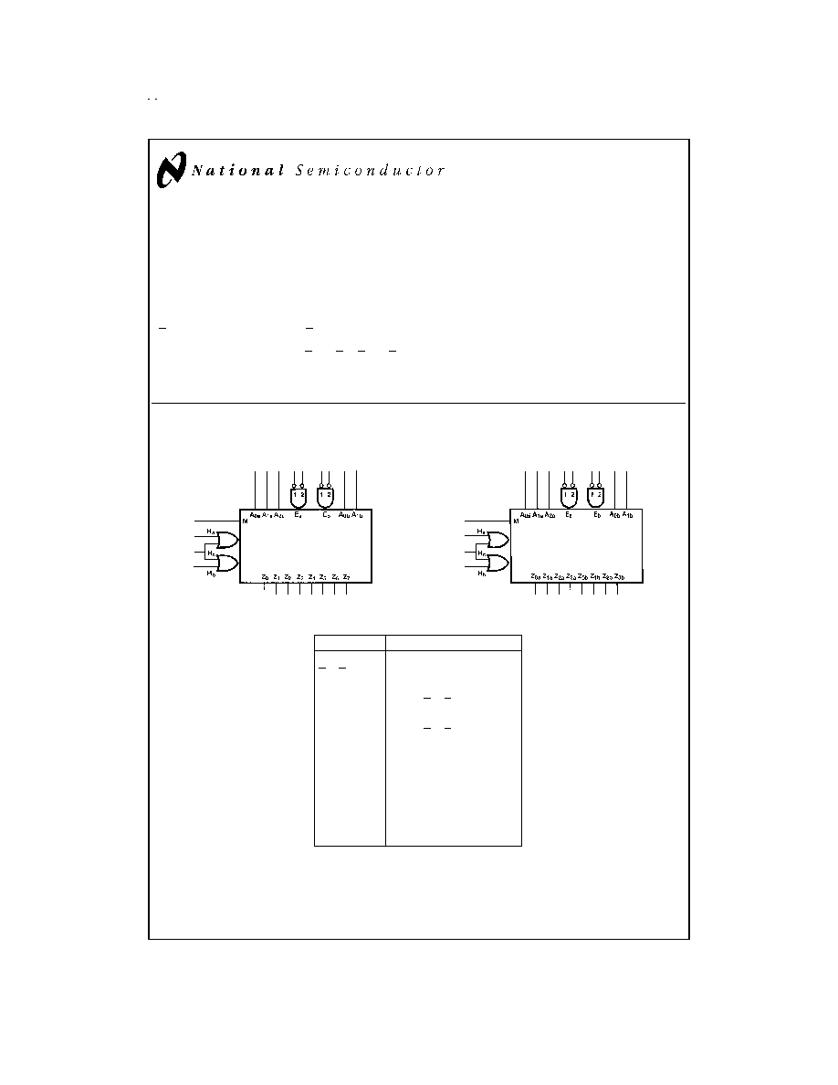
Single 1-of 8 Application
DS100311-1
Dual 1-of-4 Application
DS100311-4
August 1998
100370
Low
Power
Universal
Demultiplexer/Decoder
© 1998 National Semiconductor Corporation
DS100311
www.national.com
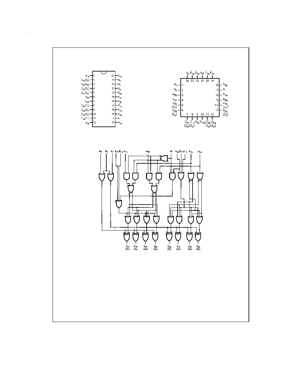
Connection Diagrams
Logic Diagram
24-Pin DIP
DS100311-2
24-Pin Quad Cerpak
DS100311-3
DS100311-6
Note 1: (Z
n
) for 1-of-4 applications.
www.national.com
2
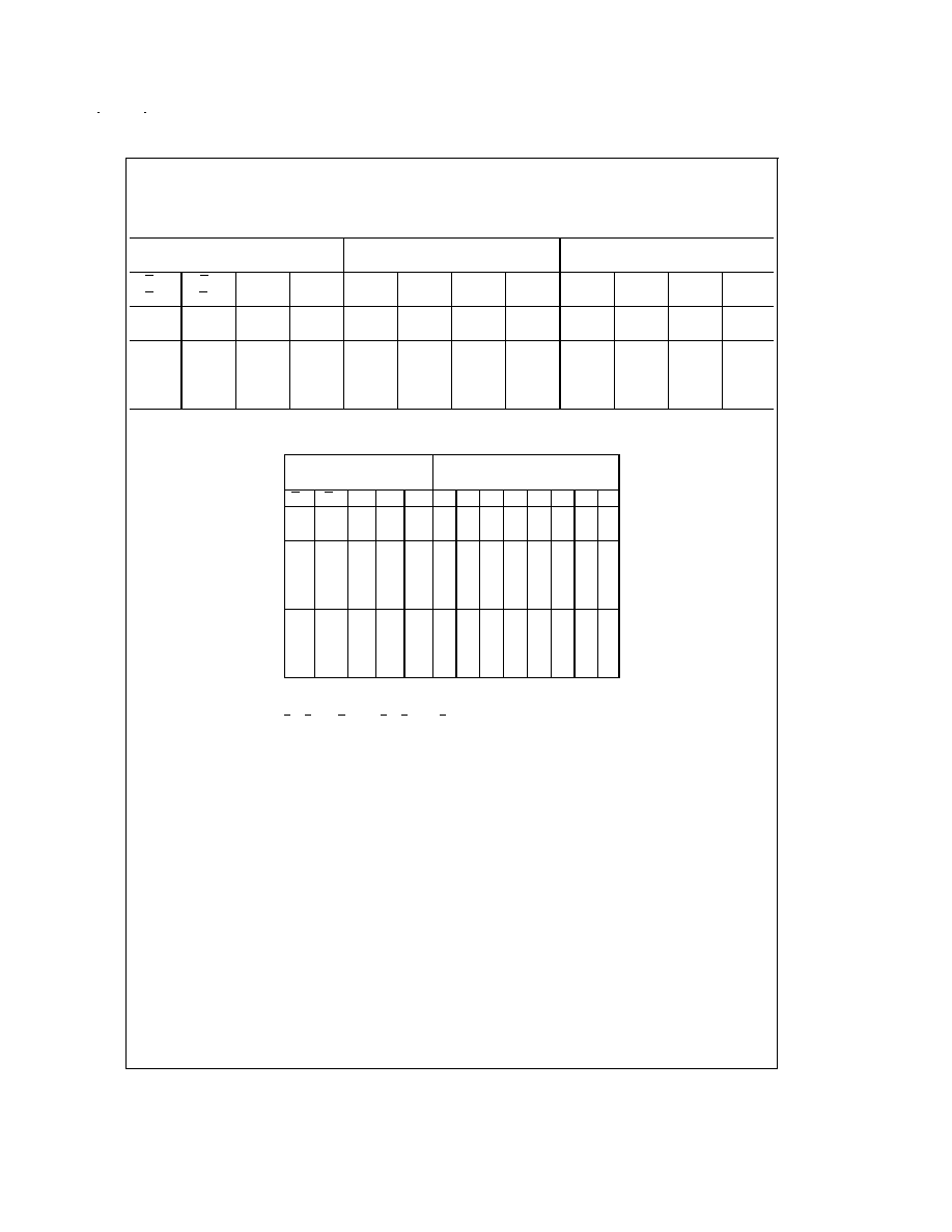
Truth Tables
Dual 1-of-4 Mode (M = A
2a
= H
c
= LOW)
Inputs
Active HIGH Outputs
Active LOW Outputs
(H
a
and H
b
Inputs HIGH)
(H
a
and H
b
Inputs LOW)
E
1a
E
2a
A
1a
A
0a
Z
0a
Z
1a
Z
2a
Z
3a
Z
0a
Z
1a
Z
2a
Z
3a
E
1b
E
2b
A
1b
A
0b
Z
0b
Z
1b
Z
2b
Z
3b
Z
0b
Z
1b
Z
2b
Z
3b
H
X
X
X
L
L
L
L
H
H
H
H
X
H
X
X
L
L
L
L
H
H
H
H
L
L
L
L
H
L
L
L
L
H
H
H
L
L
L
H
L
H
L
L
H
L
H
H
L
L
H
L
L
L
H
L
H
H
L
H
L
L
H
H
L
L
L
H
H
H
H
L
Single 1-of-8 Mode (M = HIGH; A
0b
= A
1b
= H
a
= H
b
= LOW)
Inputs
Active HIGH Outputs (Note 2)
(H
c
Input HIGH)
E
1
E
2
A
2a
A
1a
A
0a
Z
0
Z
1
Z
2
Z
3
Z
4
Z
5
Z
6
Z
7
H
X
X
X
X
L
L
L
L
L
L
L
L
X
H
X
X
X
L
L
L
L
L
L
L
L
L
L
L
L
L
H
L
L
L
L
L
L
L
L
L
L
L
H
L
H
L
L
L
L
L
L
L
L
L
H
L
L
L
H
L
L
L
L
L
L
L
L
H
H
L
L
L
H
L
L
L
L
L
L
H
L
L
L
L
L
L
H
L
L
L
L
L
H
L
H
L
L
L
L
L
H
L
L
L
L
H
H
L
L
L
L
L
L
L
H
L
L
L
H
H
H
L
L
L
L
L
L
L
H
H = HIGH Voltage Level
L = LOW Voltage Level
X = Don't Care
E
1
= E
1a
and E
1b
wired; E
2
= E2
2a
and E
2b
wired
Note 2: for H
c
= LOW, output states are complemented
www.national.com
3

Absolute Maximum Ratings
(Note 3)
If Military/Aerospace specified devices are required,
please contact the National Semiconductor Sales Office/
Distributors for availability and specifications.
Above which the useful life may be impaired.
Storage Temperature (T
STG
)
-65įC to +150įC
Maximum Junction Temperature (T
J
)
Ceramic
+175įC
V
EE
Pin Potential to Ground Pin
-7.0V to +0.5V
Input Voltage (DC)
V
EE
to +0.5V
Output Current (DC Output HIGH)
-50 mA
ESD (Note 4)
2000V
Recommended Operating
Conditions
Case Temperature (T
C
)
Military
-55įC to +125įC
Supply Voltage (V
EE
)
-5.7V to -4.2V
Note 3: Absolute maximum ratings are those values beyond which the de-
vice may be damaged or have its useful life impaired. Functional operation
under these conditions is not implied.
Note 4: ESD testing conforms to MIL-STD-883, Method 3015.
Military Version
DC Electrical Characteristics
V
EE
= -4.2V to -5.7V, V
CC
= V
CCA
= GND, T
C
= -55įC to +125įC
Symbol
Parameter
Min
Max
Units
T
C
Conditions
Notes
-1025
-870
mV
0įC to
V
OH
Output HIGH Voltage
+125įC
-1085
-870
mV
-55įC
V
IN
= V
IH
(Max)
Loading with
(Notes 5, 6, 7)
-1830
-1620
mV
0įC to
or V
IL
(Min)
50
to -2.0V
V
OL
Output LOW Voltage
+125įC
-1830
-1555
mV
-55įC
-1035
mV
0įC to
V
OHC
Output HIGH Voltage
+125įC
-1085
mV
-55įC
V
IN
= V
IH
(Min)
Loading with
(Notes 5, 6, 7)
-1610
mV
0įC to
or V
IL
(Max)
50
to -2.0V
V
OLC
Output LOW Voltage
+125įC
-1555
mV
-55įC
V
IH
Input HIGH Voltage
-1165
-870
mV
-55įC to
Guaranteed HIGH Signal for
(Notes 5, 6, 7, 8)
+125įC
All Inputs
V
IL
Input LOW Voltage
-1830
-1475
mV
-55įC to
Guaranteed LOW Signal for
(Notes 5, 6, 7, 8)
+125įC
All Inputs
I
IL
Input LOW Current
0.50
ĶA
-55įC to
V
EE
= -4.2V
(Notes 5, 6, 7)
+125įC
V
IN
= V
IL
(Min)
I
IH
Input HIGH Current
240
ĶA
25įC to
+125įC
V
EE
= -5.7V
(Notes 5, 6, 7)
340
ĶA
-55įC
V
IN
= V
IH
(Max)
I
EE
Power Supply Current
-105
-36
mA
-55įC to
Inputs Open
(Notes 5, 6, 7)
+125įC
Note 5: F100K 300 Series cold temperature testing is performed by temperature soaking (to guarantee junction temperature equals -55įC, then testing immediately
without allowing for the junction temperature to stabilize due to heat dissipation after power-up. This provides "cold start" specs which can be considered a worst case
condition at cold temperatures.
Note 6: Screen tested 100% on each device at -55įC, +25įC, and +125įC, Subgroups 1, 2, 3, 7, and 8.
Note 7: Sample tested (Method 5005, Table I) on each manufactured lot at -55įC, +25įC, and +125įC, Subgroups A1, 2, 3, 7, and 8.
Note 8: Guaranteed by applying specific input condition and testing V
OH
/V
OL
.
www.national.com
4
AC Electrical Characteristics
V
EE
= -4.2V to -5.7V, V
CC
= V
CCA
= GND
Symbol
Parameter
T
C
= -55įC
T
C
= +25įC
T
C
= +125įC
Units
Conditions
Notes
Min
Max
Min
Max
Min
Max
t
PLH
Propagation Delay
0.3
2.40
0.4
2.20
0.40
2.70
ns
t
PHL
E
na
, E
nb
to Output
t
PLH
Propagation Delay
0.30
2.60
0.40
2.40
0.40
2.90
ns
t
PHL
A
na
, A
nb
to Output
(Notes 9, 10,
11)
t
PLH
Propagation Delay
0.30
2.60
0.40
2.40
0.40
2.40
ns
Figures 1, 2
t
PHL
H
a
, H
b
, H
c
to Output
t
PLH
Propagation Delay
0.40
3.10
0.60
2.80
0.70
3.70
ns
t
PHL
M to Output
t
TLH
Transition Time
0.30
1.60
0.30
1.60
0.30
1.60
ns
(Note 12)
t
THL
20% to 80%, 80% to 20%
Note 9: F100K 300 Series cold temperature testing is performed by temperature soaking (to guarantee junction temperature equals -55įC), then testing immediately
without allowing for the junction temperature to stabilize due to heat dissipation after power-up. This provides "cold start" specs which can be considered a worst case
condition at cold temperatures.
Note 10: Screen tested 100% on each device at +25įC, temperature only, Subgroup A9.
Note 11: Sample tested (Method 5005, Table I) on each Mfg. lot at +25įC, Subgroup A9, and at +125įC, and -55įC Temp., Subgroups A10 and A11.
Note 12: Not tested at +25įC, +125įC and -55įC Temperature (design characterization data).
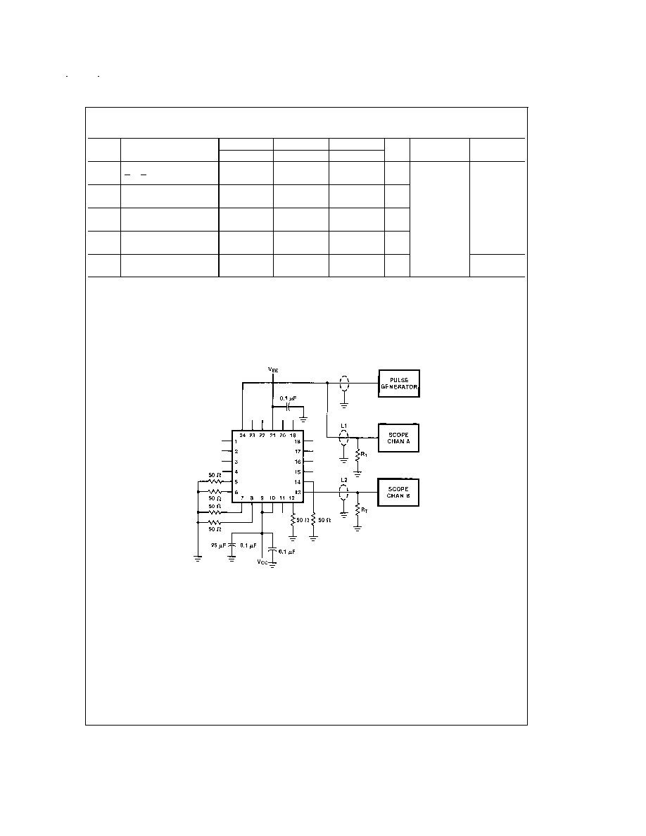
Test Circuit
DS100311-7
Notes:
V
CC
, V
CCA
= +2V, V
EE
= -2.5V
L1 and L2 = equal length 50
impedance lines
R
T
= 50
terminator internal to scope
Decoupling 0.1 ĶF from GND to V
CC
and V
EE
All unused outputs are loaded with 50
to GND
C
L
= Fixture and stray capacitance
3 pF
Pin numbers shown are for flatpak; for DIP see logic symbol
FIGURE 1. AC Test Circuit
www.national.com
5