 | –≠–ª–µ–∫—Ç—Ä–æ–Ω–Ω—ã–π –∫–æ–º–ø–æ–Ω–µ–Ω—Ç: 11C06FCQR | –°–∫–∞—á–∞—Ç—å:  PDF PDF  ZIP ZIP |
TL F 9890
11C06
750
MHz
D-Type
Flip-Flop
Not Intended For New Designs
August 1992
11C06
750 MHz D-Type Flip-Flop
General Description
The 11C06 is a high-speed ECL D-Type Master-Slave Flip-
Flop capable of toggle rates over 750 MHz Designed pri-
marily for high-speed prescaling it can also be used in any
application which does not require preset inputs The circuit
is voltage-compensated which makes input thresholds and
output levels insensitive to V
EE
variations Complementary
Q and Q outputs are provided as are two Data inputs Clock
and Clock Enable inputs The 11C06 is pin-compatible with
the Motorola MC1690L but is a higher-frequency replace-
ment
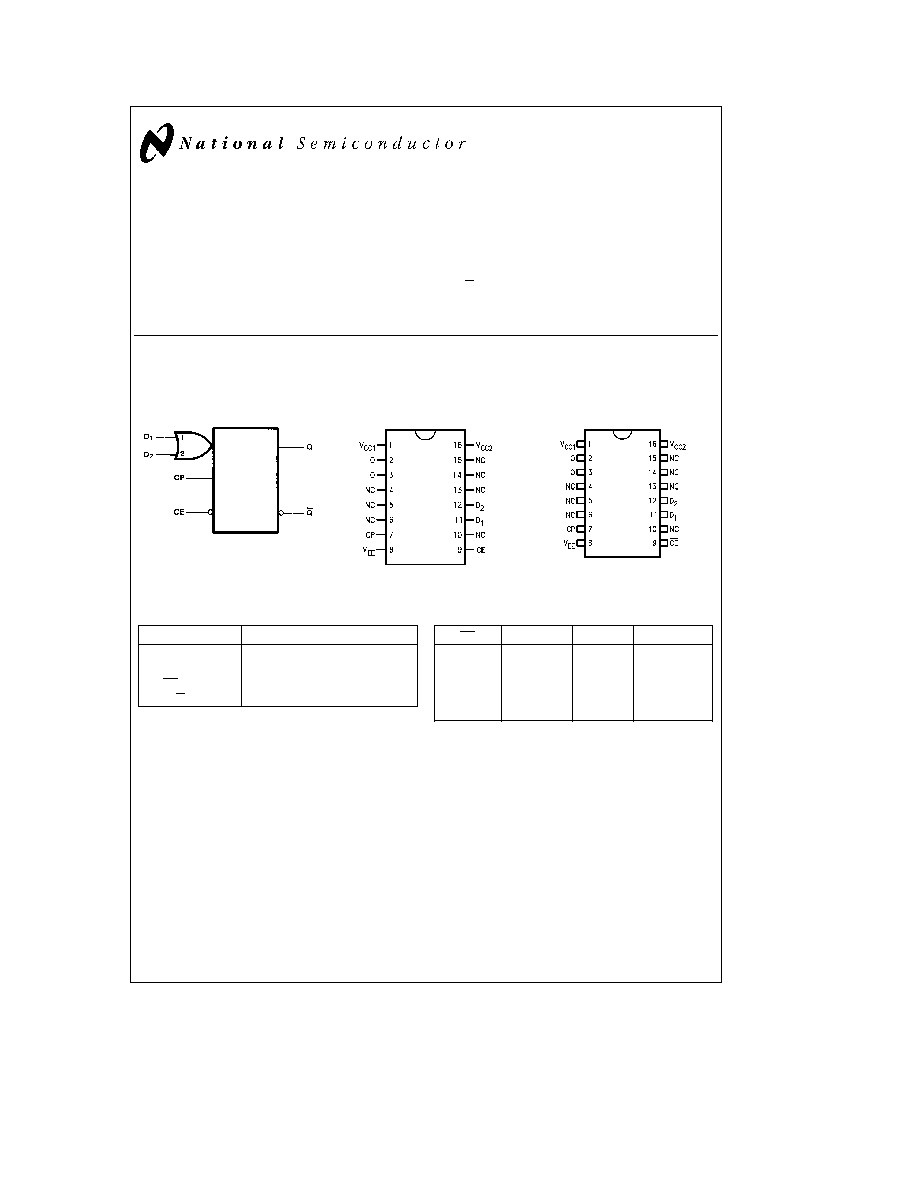
Logic Symbol
Connection Diagrams
TL F 9890 ≠ 3
16-Pin DIP
TL F 9890 ≠ 1
16-Pin Flatpak
TL F 9890 ≠ 2
Pin Names
Description
D
n
Data Input
CP
Clock Input
CE
Clock Enable (Active LOW)
Q Q
Outputs
Truth Table
CE
CP
D
Q
n
L
L
X
Q
nb1
L
H
X
Q
nb1
L
L
L
L
L
L
H
H
H
X
X
Q
nb1
H
e
HIGH Voltage Level
L
e
LOW Voltage Level
X
e
Don't Care
L
e
LOW to HIGH Transition
Q
n
b
1
e
Previous State
C1995 National Semiconductor Corporation
RRD-B30M115 Printed in U S A
Absolute Maximum Ratings
Above which the useful life may be impaired
If Military Aerospace specified devices are required
please contact the National Semiconductor Sales
Office Distributors for availability and specifications
Storage Temperature
b
65 C to
a
150 C
Maximum Junction Temperature (T
J
)
a
150 C
Supply Voltage Range
b
7 0V to GND
Input Voltage (DC)
V
EE
to GND
Output Current (DC Output HIGH)
b
50 mA
Operating Range
b
5 7V to
b
4 7V
Lead Temperature (Soldering 10 sec )
300 C
Recommended Operating
Conditions
Min
Typ
Max
Supply Voltage (V
EE
)
b
5 7V
b
5 2V
b
4 7V
Ambient Temperature (T
A
)
0 C
a
75 C
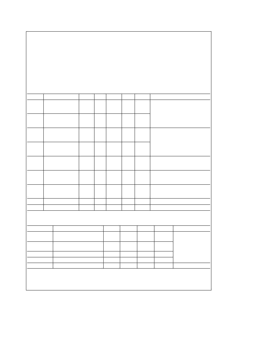
DC Electrical Characteristics
V
EE
e b
5 2V V
CC
e
GND
Symbol
Parameter
Min
Typ
Max
Units
T
A
Conditions
V
OH
Output Voltage HIGH
b
1000
b
840
mV
0 C
V
IN
e
V
IH (Max)
or V
IL (Min)
per Truth
b
960
b
810
mV
a
25 C
Table Loading 50X to
b
2V
b
900
b
720
mV
a
75 C
V
OL
Output Voltage LOW
b
1870
b
1635
mV
0 C
b
1850
b
1620
mV
a
25 C
b
1830
b
1595
mV
a
75 C
V
OHC
Output Voltage HIGH
b
1020
mV
0 C
V
IN
e
V
IH (Min)
or V
IL (Max)
for D
n
Inputs
b
980
mV
a
25 C
Loading 50X to
b
2V
b
920
mV
a
75 C
V
OLC
Output Voltage LOW
b
1615
mV
0 C
b
1600
mV
a
25 C
b
1575
mV
a
75 C
V
IH
Input Voltage HIGH
b
1135
b
840
mV
0 C
Guaranteed Input Voltage HIGH
b
1095
b
810
mV
a
25 C
for All Inputs
b
1035
b
720
mV
a
75 C
V
IL
Input Voltage LOW
b
1870
b
1500
mV
0 C
Guaranteed Input Voltage LOW
b
1850
b
1485
mV
a
25 C
for All Inputs
b
1830
b
1460
mV
a
75 C
I
IH
Input Current HIGH
V
IN
e
V
IH (Max)
Clock Input
250
m
A
a
25 C
Data Input
270
m
A
a
25 C
I
IL
Input Current LOW
0 5
m
A
a
25 C
V
IN
e
V
IH (Min)
I
EE
Power Supply Current
b
59
b
40
mA
a
25 C
All Inputs Open
AC Electrical Characteristics
V
EE
e b
5 2V V
CC
e
GND T
A
e a
25 C
Symbol
Parameter
Min
Typ
Max
Units
Conditions
t
PHL
Propagation Delay (CP-Q)
0 7
1 0
1 2
ns
t
PLH
Propagation Delay (CP-Q)
0 7
1 0
1 2
ns
t
TLH
Transition Time 20% to 80%
0 5
0 8
1 0
ns
See
Figure 1
t
THL
Transition Time 80% to 20%
0 5
0 8
1 0
ns
t
S
Set-up Time
0 2
ns
t
H
Hold Time
0 2
ns
f
TOG (MAX)
Toggle Frequency (CP)
650
750
MHz
See
Figure 2 Note
Note
The device is guaranteed for f
TOG
(CP)
t
600 MHz f
TOG
(CE)
t
550 MHz over the 0 C to
a
75 C temperature range
2
Functional Description
While the clock is LOW the slave is held steady and the
information on the D input is permitted to enter the master
The next transition from LOW to HIGH locks the master in
its present state making it insensitive to the D input This
transition simultaneously connects the slave to the master
causing the new information to appear on the outputs Mas-
ter and slave clock thresholds are internally offset in oppo-
site directions to avoid race conditions or simultaneous
master-slave changes when the clock has slow rise or fall
times
The CP and CE inputs are logically identical but physical
constraints associated with the Dual-In-Line package make
the CE input slower at the upper end of the toggle range To
prevent new data from entering the master on the next CP
LOW cycle CE should go HIGH while CP is still HIGH
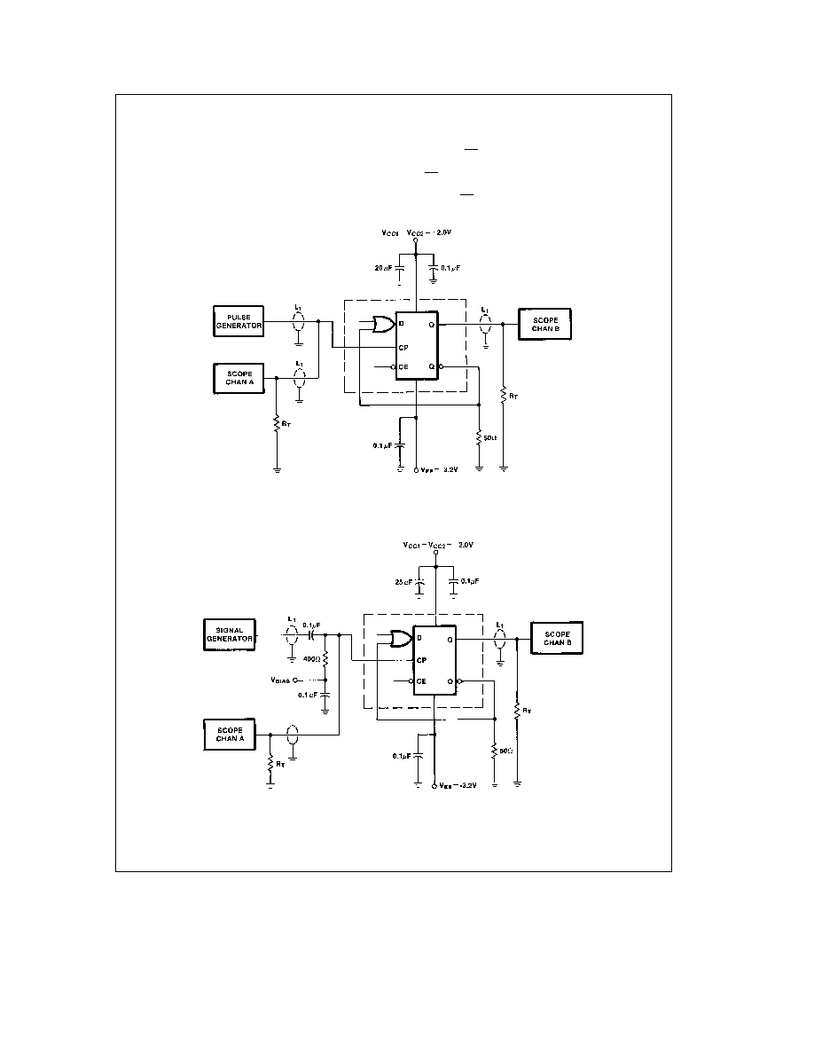
TL F 9890 ≠ 4
R
T
e
50X termination of scope
L
1
e
50X impedance lines
All input transition times are 2 0 ns
g
0 2 ns
FIGURE 1 Propagation Delay (CP to Q)
TL F 9890 ≠ 5
R
T
e
50X termination of scope
L
1
e
50X impedance lines
Adjust V
BIAS
for
a
0 7V baseline of
800 mV peak-to-peak sinewave input
All input transition times are 2 0 ns
g
0 2 ns
FIGURE 2 Toggle Frequency Test Circuit
3
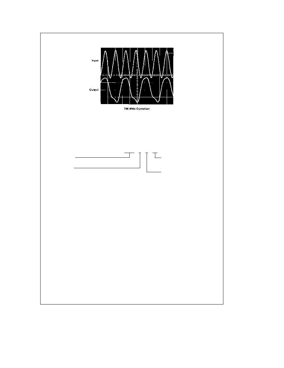
Typical Waveforms
TL F 9890 ≠ 6
Horizontal Scale
e
1 0 ns div
Vertical Scale
e
200 mV div
Ordering Information
The device number is used to form part of a simplified purchasing code where the package type and temperature range are
defined as follows
11C06
D
C
QR
Device Number
Special Variations
(basic)
QR
e
Commercial grade device
with burn-in
Package Code
D
e
Ceramic Dual-In-Line
Temperature Range
F
e
Flatpak
C
e
Commercial (0 C to
a
85 C)
4

Physical Dimensions
inches (millimeters)
16 Lead Ceramic Dual-In-Line Package (D)
NS Package Number J16A
5