TL F 6538
54121DM54121DM74121
One-Shot
with
Clear
and
Complementary
Outputs
June 1989
54121 DM54121 DM74121 One-Shot with
Clear and Complementary Outputs
General Description
The DM54 74121 is a monostable multivibrator featuring
both positive and negative edge triggering with complemen-
tary outputs An internal 2kX timing resistor is provided for
design convenience minimizing component count and lay-
out problems This device can be used with a single external
capacitor Inputs (A) are active-low trigger transition inputs
and input (B) is an active-high transition Schmitt-trigger in-
put that allows jitter-free triggering from inputs with tran-
sition rates as slow as 1 volt second A high immunity to
V
CC
noise of typically 1 5V is also provided by internal cir-
cuitry at the input stage
To obtain optimum and trouble free operation please read
operating rules and NSC one-shot application notes careful-
ly and observe recommendations
Features
Y
Triggered from active-high transition or active-low tran-
sition inputs
Y
Variable pulse width from 30 ns to 28 seconds
Y
Jitter free Schmitt-trigger input
Y
Excellent noise immunity typically 1 2V
Y
Stable pulse width up to 90% duty cycle
Y
TTL DTL compatible
Y
Compensated for V
CC
and temperature variations
Y
Input clamp diodes
Y
Alternate Military Aerospace device (54121) is avail-
able Contact a National Semiconductor Sales Office
Distributor for specifications
Functional Description
The basic output pulse width is determined by selection of
an internal resistor R
INT
or an external resistor (R
X
) and
capacitor (C
X
) Once triggered the output pulse width is in-
dependent of further transitions of the inputs and is a func-
tion of the timing components Pulse width can vary from a
few nano-seconds to 28 seconds by choosing appropriate
R
X
and C
X
combinations There are three trigger inputs from
the device two negative edge-triggering (A) inputs one pos-
itive edge Schmitt-triggering (B) input
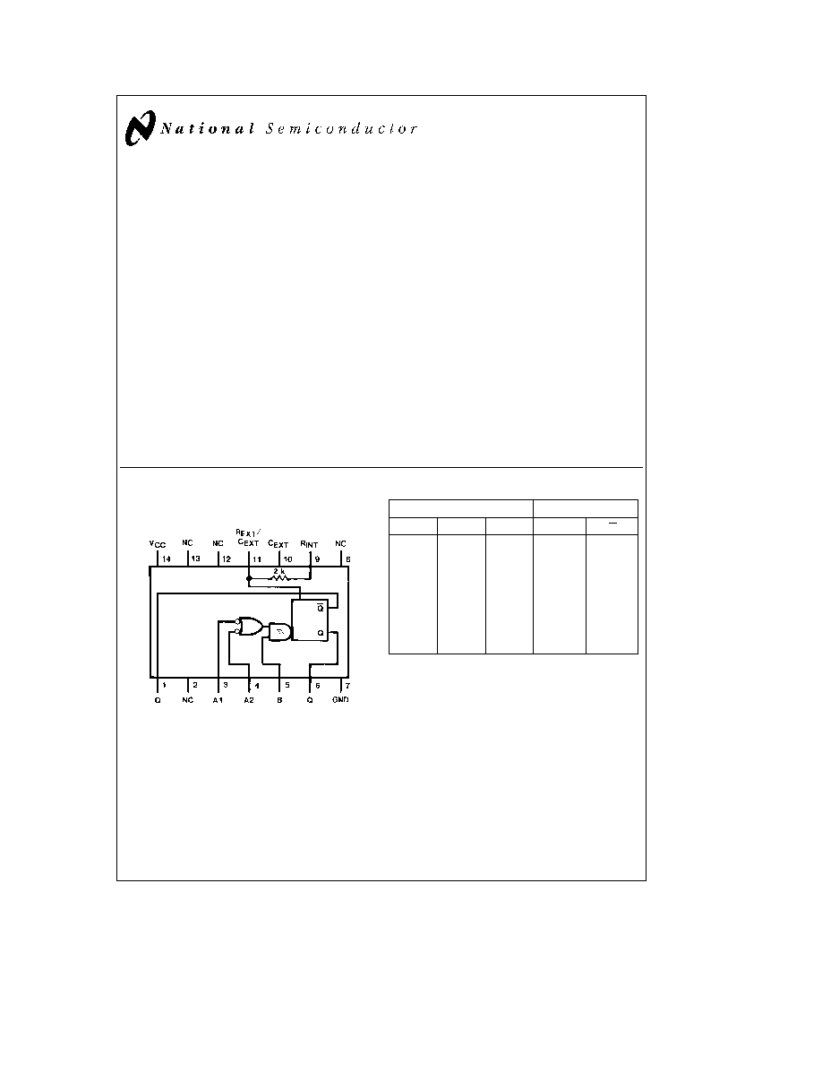
Connection Diagram
Dual-In-Line Package
TL F 6538 � 1
Order Number 54121DMQB 54121FMQB
DM54121J DM54121W or DM74121N
See NS Package Number J14A N14A or W14B
Function Table
Inputs
Outputs
A1
A2
B
Q
Q
L
X
H
L
H
X
L
H
L
H
X
X
L
L
H
H
H
X
L
H
H
v
H
v
H
H
v
v
H
L
X
u
X
L
u
H
e
High Logic Level
L
e
Low Logic Level
X
e
Can Be Either Low or High
u
e
Positive Going Transition
v
e
Negative Going Transition
e
A Positive Pulse
e
A Negative Pulse
C1995 National Semiconductor Corporation
RRD-B30M105 Printed in U S A
Absolute Maximum Ratings
(Note)
If Military Aerospace specified devices are required
please contact the National Semiconductor Sales
Office Distributors for availability and specifications
Supply Voltage
7V
Input Voltage
5 5V
Operating Free Air Temperature Range
DM54
b
55 C to
a
125 C
DM74
0 C to
a
70 C
Storage Temperature Range
b
65 C to
a
150 C
Note
The ``Absolute Maximum Ratings'' are those values
beyond which the safety of the device cannot be guaran-
teed The device should not be operated at these limits The
parametric values defined in the ``Electrical Characteristics''
table are not guaranteed at the absolute maximum ratings
The ``Recommended Operating Conditions'' table will define
the conditions for actual device operation
Recommended Operating Conditions
Symbol
Parameter
DM54121
DM74121
Units
Min
Nom
Max
Min
Nom
Max
V
CC
Supply Voltage
4 5
5
5 5
4 75
5
5 25
V
V
Ta
Positive-Going Input Threshold
1 4
2
1 4
2
V
Voltage at the A Input (V
CC
e
Min)
V
Tb
Negative-Going Input Threshold
0 8
1 4
0 8
1 4
V
Voltage at the A Input (V
CC
e
Min)
V
Ta
Positive-Going Input Threshold
1 5
2
1 5
2
V
Voltage at the B Input (V
CC
e
Min)
V
Tb
Negative-Going Input Threshold
0 8
1 3
0 8
1 3
V
Voltage at the B Input (V
CC
e
Min)
I
OH
High Level Output Current
b
0 4
b
0 4
mA
I
OL
Low Level Output Current
16
16
mA
t
W
Input Pulse Width (Note 1)
40
40
ns
dV dt
Rate of Rise or Fall of
1
1
V s
Schmidt Input (B) (Note 1)
dV dt
Rate of Rise or Fall of
1
1
V ms
Logic Input (A) (Note 1)
R
EXT
External Timing Resistor (Note 1)
1 4
30
1 4
40
kX
C
EXT
External Timing Capacitance (Note 1)
0
1000
0
1000
m
F
DC
Duty Cycle (Note 1)
R
T
e
2 kX
67
67
%
R
T
e
R
EXT
(Max)
90
90
T
A
Free Air Operating Temperature
b
55
125
0
70
C
Note 1
T
A
e
25 C and V
CC
e
5V
Electrical Characteristics
over recommended operating free air temperature range (unless otherwise noted)
Symbol
Parameter
Conditions
Min
Typ
Max
Units
(Note 1)
V
I
Input Clamp Voltage
V
CC
e
Min I
I
e b
12 mA
b
1 5
V
V
OH
High Level Output
V
CC
e
Min I
OH
e
Max
2 4
3 4
V
Voltage
V
IL
e
Max V
IH
e
Min
V
OL
Low Level Output
V
CC
e
Min I
OL
e
Max
0 2
0 4
V
Voltage
V
IH
e
Min V
IL
e
Max
I
I
Input Current
Max
V
CC
e
Max V
I
e
5 5V
1
mA
Input Voltage
I
IH
High Level Input
V
CC
e
Max
A1 A2
40
m
A
Current
V
I
e
2 4V
B
80
I
IL
Low Level Input
V
CC
e
Max
A1 A2
b
1 6
mA
Current
V
I
e
0 4V
B
b
3 2
I
OS
Short Circuit
V
CC
e
Max
DM54
b
20
b
55
mA
Output Current
(Note 2)
DM74
b
18
b
55
I
CC
Supply Current
V
CC
e
Max
Quiescent
13
25
mA
Triggered
23
40
Note 1
All typicals are at V
CC
e
5V T
A
e
25 C
Note 2
Not more than one output should be shorted at a time
2
Switching Characteristics
at V
CC
e
5V and T
A
e
25 C (See Section 1 for Test Waveforms and Outout Load)
Symbol
Parameter
From (Input)
Conditions
Min
Max
Units
To (Output)
t
PLH
Propagation Delay Time
A1 A2
C
EXT
e
80 pF
70
ns
Low to High Level Output
to Q
R
INT
to V
CC
t
PLH
Propagation Delay Time
B to
C
L
e
15 pF
55
ns
Low to High Level Output
Q
R
L
e
400X
t
PHL
Propagation Delay Time
A1 A2
80
ns
High to Low Level Output
to Q
t
PHL
Propagation Delay Time
B
65
ns
High to Low Level Output
to Q
t
W(OUT)
Output Pulse
A1 A2 or B
C
EXT
e
80 pF
Width Using the
to Q Q
R
INT
to V
CC
70
150
ns
Internal Timing Resistor
R
L
e
400X
C
L
e
15 pF
t
W(OUT)
Output Pulse
A1 A2
C
EXT
e
0 pF
Width Using Zero
to Q Q
R
INT
to V
CC
50
ns
Timing Capacitance
R
L
e
400X
C
L
e
15 pF
t
W(OUT)
Output Pulse
A1 A2
C
EXT
e
100 pF
Width Using External
to Q Q
R
INT
e
10 kX
600
800
ns
Timing Resistor
R
L
e
400X
C
L
e
15 pF
A1 A2
C
EXT
e
1 mF
to Q Q
R
INT
e
10 kX
6
8
ms
R
L
e
400X
C
L
e
15 pF
Operating Rules
1 To use the internal 2 kX timing resistor connect the R
INT
pin to V
CC
2 An external resistor (R
X
) or the internal resistor (2 kX)
and an external capacitor (C
X
) are required for proper
operation The value of C
X
may vary from 0 to any neces-
sary value For small time constants use high-quality
mica glass polypropylene polycarbonate or polystyrene
capacitors For large time constants use solid tantalum or
special aluminum capacitors If the timing capacitors
have leakages approaching 100 nA or if stray capaci-
tance from either terminal to ground is greater than 50 pF
the timing equations may not represent the pulse width
the device generates
3 The pulse width is essentially determined by external tim-
ing components R
X
and C
X
For C
X
k
1000 pF see
Fig-
ure 1 design curves on T
W
as function of timing compo-
nents value For C
X
l
1000 pF the output is defined as
t
W
e
K R
X
C
X
where R
X
is in Kilo-ohm
C
X
is in pico Farad
T
W
is in nano second
K
0 7
TL F 6538 � 2
FIGURE 1
4 If C
X
is an electrolytic capacitor a switching diode is often
required for standard TTL one-shots to prevent high in-
verse leakage current
(Figure 2)
TL F 6538 � 3
FIGURE 2
3
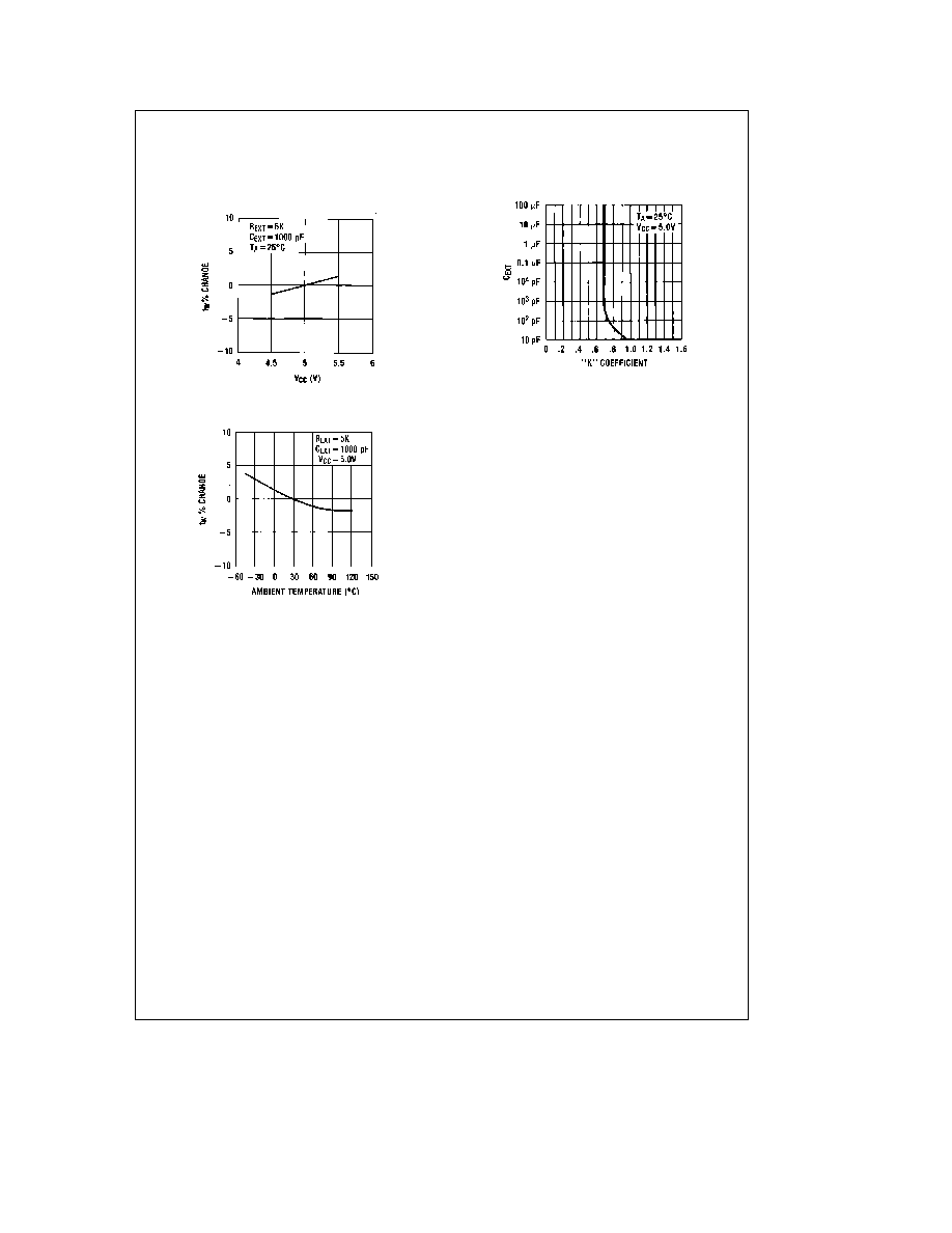
Operating Rules
(Continued)
5 Output pulse width versus V
CC
and operation tempera-
tures
Figure 3 depicts the relationship between pulse
width variation versus V
CC
Figure 4 depicts pulse width
variation versus ambient temperature
TL F 6538 � 4
FIGURE 3
TL F 6538 � 5
FIGURE 4
6 The ``K'' coefficient is not a constant but varies as a
function of the timing capacitor C
X
Figure 5 details this
characteristic
TL F 6538 � 6
FIGURE 5
7 Under any operating condition C
X
and R
X
must be kept
as close to the one-shot device pins as possible to mini-
mize stray capacitance to reduce noise pick-up and to
reduce I
c
R and Ldi dt voltage developed along their
connecting paths If the lead length from C
X
to pins (10)
and (11) is greater than 3 cm for example the output
pulse width might be quite different from values predicted
from the appropriate equations A non-inductive and low
capacitive path is necessary to ensure complete dis-
charge of C
X
in each cycle of its operation so that the
output pulse width will be accurate
8 V
CC
and ground wiring should conform to good high-fre-
quency standards and practices so that switching tran-
sients on the V
CC
and ground return leads do not cause
interaction between one-shots A 0 01 mF to 0 10 mF by-
pass capacitor (disk ceramic or monolithic type) from V
CC
to ground is necessary on each device Furthermore the
bypass capacitor should be located as close to the V
CC
-
pin as space permits
For further detailed device characteristics and output performance please
refer to the NSC one-shot application note AN-366
4
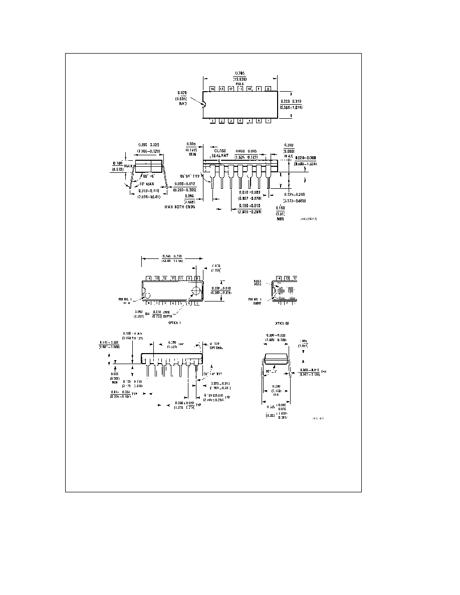
Physical Dimensions
inches (millimeters)
14-Lead Ceramic Dual-In-Line Package (J)
Order Number 54121DMQB or DM54121J
NS Package Number J14A
14-Lead Molded Dual-In-Line Package (N)
Order Number DM74121N
NS Package Number N14A
5