 | –≠–ª–µ–∫—Ç—Ä–æ–Ω–Ω—ã–π –∫–æ–º–ø–æ–Ω–µ–Ω—Ç: 54122 | –°–∫–∞—á–∞—Ç—å:  PDF PDF  ZIP ZIP |
TL F 10212
54122DM74122
Retriggerable
Resettable
Multivibrator
June 1989
54122 DM74122
Retriggerable Resettable Multivibrator
General Description
The '122 features positive and negative DC level triggering
inputs complementary outputs an optional 10 kX internal
timing resistor and an overriding Direct Clear (C
D
) input
When the circuit is in the quasi-stable (delay) state another
trigger applied to the inputs (per Truth Table) will cause the
delay period to start again without disturbing the outputs
This process can be repeated indefinitely and thus the out-
put pulse period (Q HIGH Q LOW) can be made as long as
desired Alternatively a delay period can be terminated
by a LOW signal applied to C
D
which also prevents trigger-
ing An internal connection from C
D
to the input gate makes
it possible to trigger the circuit by a positive-going signal on
C
D
as shown in the Truth Table For timing capacitor values
greater than 1000 pF the output pulse width is defined as
follows
t
w
e
0 32 R
X
C
X
(1 0
a
0 7 R
X
)
Where t
w
is in ns R
X
is in kX and C
X
is in pF
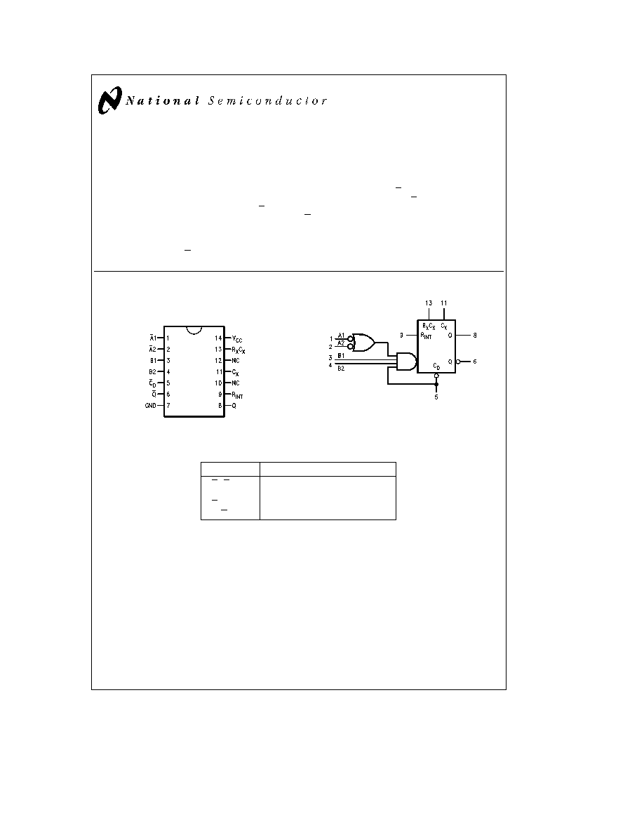
Connection Diagram
Dual-In-Line Package
TL F 10212 ≠ 1
Order Number 54122DMQB 54122FMQB or DM74122N
See NS Package Number J14A N14A or W14B
Logic Symbol
TL F 10212 ≠ 2
V
CC
e
Pin 14
GND
e
Pin 7
NC
e
Pins 10 and 12
Pin Names
Description
A
1
A
2
Trigger Inputs (Active Falling Edge)
B
1
B
2
Trigger Inputs (Active Rising Edge)
C
D
Direct Clear Inputs (Active LOW)
Q Q
Outputs
C1995 National Semiconductor Corporation
RRD-B30M105 Printed in U S A
Absolute Maximum Ratings
(Note)
If Military Aerospace specified devices are required
please contact the National Semiconductor Sales
Office Distributors for availability and specifications
Supply Voltage
7V
Input Voltage
5 5V
Operating Free Air Temperature Range
54
b
55 C to
a
125 C
DM74
0 C to
a
70 C
Storage Temperature Range
b
65 C to
a
150 C
Note
The ``Absolute Maximum Ratings'' are those values
beyond which the safety of the device cannot be guaran-
teed The device should not be operated at these limits The
parametric values defined in the ``Electrical Characteristics''
table are not guaranteed at the absolute maximum ratings
The ``Recommended Operating Conditions'' table will define
the conditions for actual device operation
Recommended Operating Conditions
Symbol
Parameter
54122
DM74122
Units
Min
Nom
Max
Min
Nom
Max
V
CC
Supply Voltage
4 5
5
5 5
4 75
5
5 5
V
V
IH
High Level Input Voltage
2
2
V
V
IL
Low Level Input Voltage
0 8
0 8
V
I
OH
High Level Output Current
b
0 8
b
0 8
mA
I
OL
Low Level Output Current
16
16
mA
T
A
Free Air Operating Temperature
b
55
125
b
55
70
C
Recommended Operating Conditions
V
CC
e a
5 0V T
A
e a
25 C
Symbol
Parameter
Conditions
DM74
Units
Min
Max
t
w
Trigger Pulse Width
40
ns
R
X
External Timing Resistor
XC
Over Operating V
CC
and
5 0
50
kX
XM
Temperature Range
5 0
25
C
X
External Timing Capacitor
No Restrictions
pF
Electrical Characteristics
over recommended operating free air temperature range (unless otherwise noted)
Symbol
Parameter
Conditions
Min
Typ
Max
Units
(Note 1)
V
I
Input Clamp Voltage
V
CC
e
Min I
I
e b
12 mA
b
1 5
V
V
OH
High Level Output Voltage
V
CC
e
Min I
OH
e
Max
2 4
V
V
IL
e
Max
V
OL
Low Level Output Voltage
V
CC
e
Min V
IH
e
Min
0 4
V
I
I
Input Current
Max
V
CC
e
Max V
I
e
5 5V
1
mA
Input Voltage
I
IH
High Level Input Current
V
CC
e
Max V
I
e
2 4V
Inputs
40
m
A
Clear
80
I
IL
Low Level Input Current
V
CC
e
Max V
I
e
0 4V
Inputs
b
1 6
mA
Clear
b
3 2
I
OS
Short Circuit Output Current
V
CC
e
Max (Note 2)
b
10
b
40
mA
I
CC
Supply Current
V
CC
e
Max
28
mA
Note 1
All typicals are at V
CC
e
5V T
A
e
25 C
Note 2
Not more than one output should be shorted at a time and the duration should not exceed one second
2
Switching Characteristics
V
CC
e a
5 0V T
A
e a
25 C (See Section 3 for waveforms and load configurations)
54 74
Symbol
Parameter
Conditions
C
L
e
15 pF
Units
R
L
e
400X
Min
Max
t
PLH
Propagation Delay
28
ns
B to Q
t
PLH
Propagation Delay
33
ns
A to Q
C
X
e
0 pF R
X
e
5 kX
t
PLH
Propagation Delay
Figure 3-1 Figure a
36
ns
B to Q
t
PHL
Propagation Delay
40
ns
A to Q
t
PLH
Propagation Delay
40
ns
C
D
to Q
C
X
e
0 pF R
X
e
5 kX
t
PHL
Propagation Delay
Figure 3-1 Figure 3-10
27
ns
C
D
to Q
t
w(out)
Pulse Width at Q with Zero
C
X
e
0 pF R
X
e
5 kX
65
ns
Timing Capacitor
Figure 3-1 Figure a
t
w(out)
Pulse Width with External
C
X
e
1000 pF R
X
e
10 kX
3 08
3 76
m
s
Timing Components
Figure 3-1 Figure a
Triggering Truth Table
Inputs
Response
C
D
A
1
A
2
B
1
B
2
L
X
X
X
X
No Trigger
X
K
L
X
X
No Trigger
X
K
X
L
X
No Trigger
H
K
H
H
H
Trigger
X
X
X
L
L
No Trigger
X
H
H
L
X
No Trigger
H
L
X
L
H
Trigger
L
L
X
H
H
Trigger
H
e
HIGH Voltage Level
L
e
LOW Voltage Level
X
e
Immaterial
Input pins 1 and 2 are logically interchangeable as are input pins 3 and 4
3
Pulse Width vs R
X
and C
X
TL F 10212 ≠ 3
Timing Capacitor C
X
≠ pF
TL F 10212 ≠ 4
FIGURE A
4

Physical Dimensions
inches (millimeters)
14-Lead Ceramic Dual-In-Line Package (J)
Order Number 54122DMQB
NS Package Number J14A
14-Lead Molded Dual-In-Line Package (N)
Order Number DM74122N
NS Package Number N14A
5