TL F 6546
54150DM54150DM74150
54151ADM54151ADM74151A
Data
SelectorsMultiplexers
June 1989
54150 DM54150 DM74150
54151A DM54151A DM74151A
Data Selectors Multiplexers
General Description
These data selectors multiplexers contain full on-chip de-
coding to select the desired data source The 150 selects
one-of-sixteen data sources the 151A selects one-of-eight
data sources The 150 and 151A have a strobe input which
must be at a low logic level to enable these devices A high
level at the strobe forces the W output high and the Y output
(as applicable) low
The 151A features complementary W and Y outputs where-
as the 150 has an inverted (W) output only
The 151A incorporates address buffers which have sym-
metrical propagation delay times through the complementa-
ry paths This reduces the possibility of transients occurring
at the output(s) due to changes made at the select inputs
even when the 151A outputs are enabled (i e strobe low)
Features
Y
150 selects one-of-sixteen data lines
Y
151A selects one-of-eight data lines
Y
Performs parallel-to-serial conversion
Y
Permits multiplexing from N lines to one line
Y
Also for use as Boolean function generator
Y
Typical average propagation delay time data input to W
output
150
11 ns
151A
9 ns
Y
Typical power dissipation
150
200 mW
151A
135 mW
Y
Alternate Military Aerospace device (54150 54151A) is
available Contact a National Semiconductor Sales Of-
fice Distributor for specifications
Connection Diagrams
Dual-In-Line Package
TL F 6546 ≠ 1
Order Number 54150DQMB 54150FMQB
DM54150J or DM74150N
See NS Package Number J24A N24A or W24C
Dual-In-Line Package
TL F 6546 ≠ 2
Order Number 54151ADMQB 54151AFMQB
DM54151AJ DM54151AW or DM74151AN
See NS Package Number J16A N16E or W16A
C1995 National Semiconductor Corporation
RRD-B30M105 Printed in U S A
Absolute Maximum Ratings
(Note)
If Military Aerospace specified devices are required
please contact the National Semiconductor Sales
Office Distributors for availability and specifications
Supply Voltage
7V
Input Voltage
5 5V
Operating Free Air Temperature Range
DM54 and 54
b
55 C to
a
125 C
DM74
0 C to
a
70 C
Storage Temperature Range
b
65 C to
a
150 C
Note
The ``Absolute Maximum Ratings'' are those values
beyond which the safety of the device cannot be guaran-
teed The device should not be operated at these limits The
parametric values defined in the ``Electrical Characteristics''
table are not guaranteed at the absolute maximum ratings
The ``Recommended Operating Conditions'' table will define
the conditions for actual device operation
Recommended Operating Conditions
Symbol
Parameter
DM54150
DM74150
Units
Min
Nom
Max
Min
Nom
Max
V
CC
Supply Voltage
4 5
5
5 5
4 75
5
5 25
V
V
IH
High Level Input Voltage
2
2
V
V
IL
Low Level Input Voltage
0 8
0 8
V
I
OH
High Level Output Current
b
0 8
b
0 8
mA
I
OL
Low Level Output Current
16
16
mA
T
A
Free Air Operating Temperature
b
55
125
0
70
C
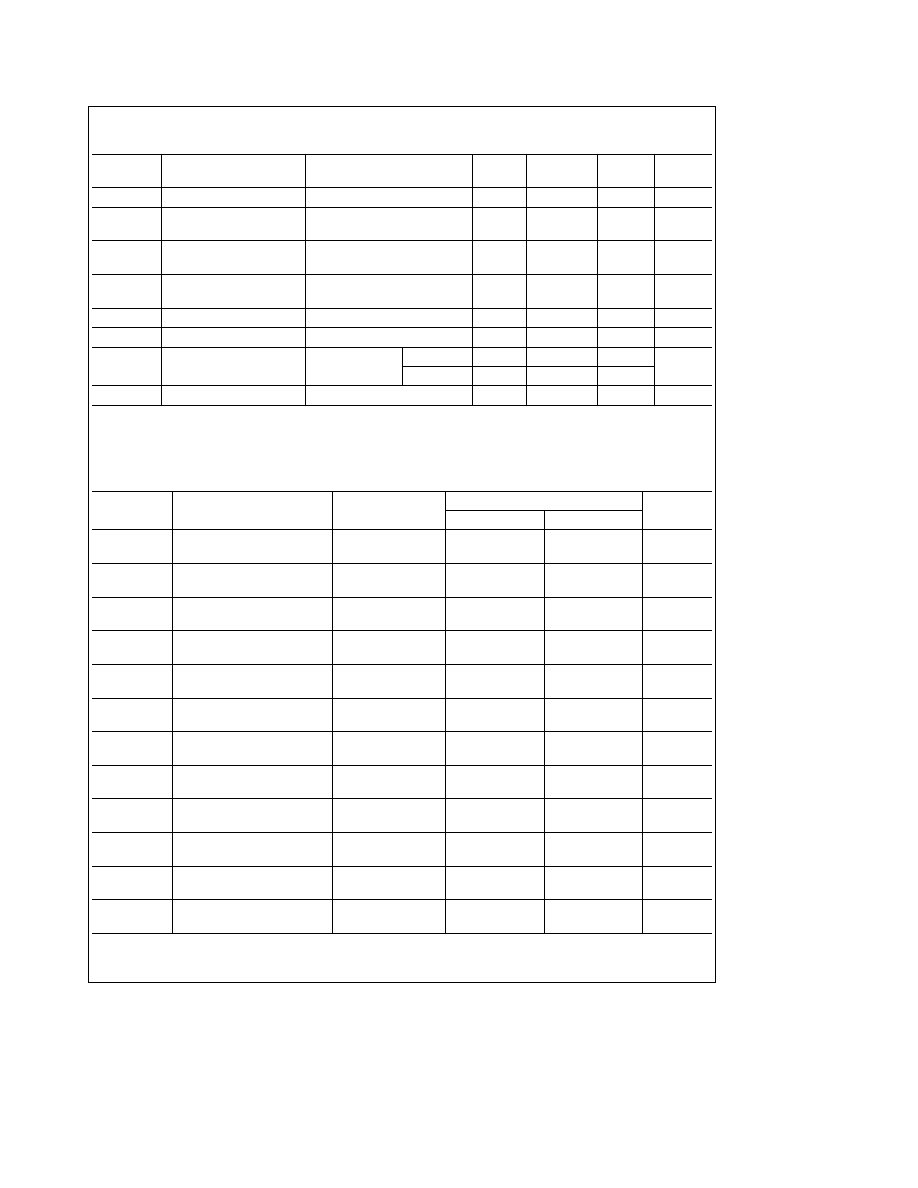
'150 Electrical Characteristics
over recommended operating free air temperature range (unless otherwise noted)
Symbol
Parameter
Conditions
Min
Typ
Max
Units
(Note 1)
V
I
Input Clamp Voltage
V
CC
e
Min I
I
e b
12 mA
b
1 5
V
V
OH
High Level Output
V
CC
e
Min I
OH
e
Max
2 4
V
Voltage
V
IL
e
Max V
IH
e
Min
V
OL
Low Level Output
V
CC
e
Min I
OL
e
Max
0 4
V
Voltage
V
IH
e
Min V
IL
e
Max
I
I
Input Current
Max
V
CC
e
Max V
I
e
5 5V
1
mA
Input Voltage
I
IH
High Level Input Current
V
CC
e
Max V
I
e
2 4V
40
m
A
I
IL
Low Level Input Current
V
CC
e
Max V
I
e
0 4V
b
1 6
mA
I
OS
Short Circuit
V
CC
e
Max
DM54
b
20
b
55
mA
Output Current
(Note 2)
DM74
b
18
b
55
I
CC
Supply Current
V
CC
e
Max (Note 3)
40
68
mA
Note 1
All typicals are at V
CC
e
5V T
A
e
25 C
Note 2
Not more than one output should be shorted at a time
Note 3
I
CC
is measured with the strobe and data select inputs at 4 5V all other inputs and outputs open
2
'150 Switching Characteristics
at V
CC
e
5V and T
A
e
25 C (See Section 1 for Test Waveforms and Output Load)
Symbol
Parameter
From (Input)
R
L
e
400X C
L
e
15 pF
Units
To (Output)
Min
Max
t
PLH
Propagation Delay Time
Select
35
ns
Low to High Level Output
to W
t
PHL
Propagation Delay Time
Select
33
ns
High to Low Level Output
to W
t
PLH
Propagation Delay Time
Strobe
24
ns
Low to High Level Output
to W
t
PHL
Propagation Delay Time
Strobe
30
ns
High to Low Level Output
to W
t
PLH
Propagation Delay Time
E0-E15
20
ns
Low to High Level Output
to W
t
PHL
Propagation Delay Time
E0-E15
14
ns
High to Low Level Output
to W
Recommended Operating Conditions
Symbol
Parameter
DM54151A
DM74151A
Units
Min
Nom
Max
Min
Nom
Max
V
CC
Supply Voltage
4 5
5
5 5
4 75
5
5 25
V
V
IH
High Level Input Voltage
2
2
V
V
IL
Low Level Input Voltage
0 8
0 8
V
I
OH
High Level Output Current
b
0 8
b
0 8
mA
I
OL
Low Level Output Current
16
16
mA
T
A
Free Air Operating Temperature
b
55
125
0
70
C
3
'151A Electrical Characteristics
over recommended operating free air temperature range (unless otherwise noted)
Symbol
Parameter
Conditions
Min
Typ
Max
Units
(Note 1)
V
I
Input Clamp Voltage
V
CC
e
Min I
I
e b
12 mA
b
1 5
V
V
OH
High Level Output
V
CC
e
Min I
OH
e
Max
2 4
V
Voltage
V
IL
e
Max V
IH
e
Min
V
OL
Low Level Output
V
CC
e
Min I
OL
e
Max
0 4
V
Voltage
V
IH
e
Min V
IL
e
Max
I
I
Input Current
Max
V
CC
e
Max V
I
e
5 5V
1
mA
Input Voltage
I
IH
High Level Input Current
V
CC
e
Max V
I
e
2 4V
40
m
A
I
IL
Low Level Input Current
V
CC
e
Max V
I
e
0 4V
b
1 6
mA
I
OS
Short Circuit
V
CC
e
Max
DM54
b
20
b
55
mA
Output Current
(Note 2)
DM74
b
18
b
55
I
CC
Supply Current
V
CC
e
Max (Note 3)
27
48
mA
Note 1
All typicals are at V
CC
e
5V T
A
e
25 C
Note 2
Not more than one output should be shorted at a time
Note 3
I
CC
is measured with the strobe and data select inputs at 4 5V all other inputs and outputs open
'151A Switching Characteristics
at V
CC
e
5V and T
A
e
25 C (See Section 1 for Test Waveforms and Output Load)
Symbol
Parameter
From (Input)
R
L
e
400X C
L
e
15 pF
Units
To (Output)
Min
Max
t
PLH
Propagation Delay Time
Select
38
ns
Low to High Level Output
(4 Levels) to Y
t
PHL
Propagation Delay Time
Select
30
ns
High to Low Level Output
(4 Levels) to Y
t
PLH
Propagation Delay Time
Select
26
ns
Low to High Level Output
(3 Levels) to W
t
PHL
Propagation Delay Time
Select
30
ns
High to Low Level Output
(3 Levels) to W
t
PLH
Propagation Delay Time
Strobe
33
ns
Low to High Level Output
to Y
t
PHL
Propagation Delay Time
Strobe
30
ns
High to Low Level Output
to Y
t
PLH
Propagation Delay Time
Strobe
21
ns
Low to High Level Output
to W
t
PHL
Propagation Delay Time
Strobe
25
ns
High to Low Level Output
to W
t
PLH
Propagation Delay Time
D0-D7
24
ns
Low to High Level Output
to Y
t
PHL
Propagation Delay Time
D0-D7
24
ns
High to Low Level Output
to Y
t
PLH
Propagation Delay Time
D0-D7
14
ns
Low to High Level Output
to W
t
PHL
Propagation Delay Time
D0-D7
14
ns
High to Low Level Output
to W
4