TL F 6556
54173DM54173DM74173
TRI-STATE
Quad
D
Registers
June 1989
54173 DM54173 DM74173
TRI-STATE
Quad D Registers
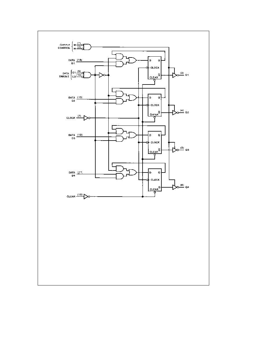
General Description
These four-bit registers contain D-type flip-flops with totem-
pole TRI-STATE outputs capable of driving highly capaci-
tive or low-impedance loads The high-impedance state and
increased high-logic-level drive provide these flip-flops with
the capability of driving the bus lines in a bus-organized sys-
tem without need for interface or pull-up components
Gated enable inputs are provided for controlling the entry of
data into the flip-flops When both data-enable inputs are
low data at the D inputs are loaded into their respective flip-
flops on the next positive transition of the buffered clock
input Gate output control inputs are also provided When
both are low the normal logic states of the four outputs are
available for driving the loads or bus lines The outputs are
disabled independently from the level of the clock by a high
logic level at either output control input The outputs then
present a high impedance and neither load nor drive the bus
line Detailed operation is given in the function table
To minimize the possibility that two outputs will attempt to
take a common bus to opposite logic levels the output con-
trol circuitry is designed so that the average output disable
times are shorter than the average output enable times
Features
Y
TRI-STATE outputs interface directly with system bus
Y
Gated output control lines for enabling or disabling the
outputs
Y
Fully independent clock elminates restrictions for oper-
ating in one of two modes
Parallel load
Do nothing (hold)
Y
For application as bus buffer registers
Y
Typical propagation delay 18 ns
Y
Typical frequency 30 MHz
Y
Typical power dissipation 250 mW
Y
Alternate Military Aerospace device (54173) is avail-
able Contact a National Semiconductor Sales Office
Distributor for specifications
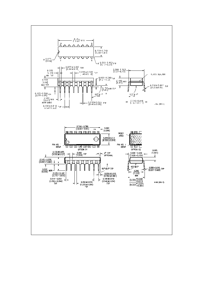
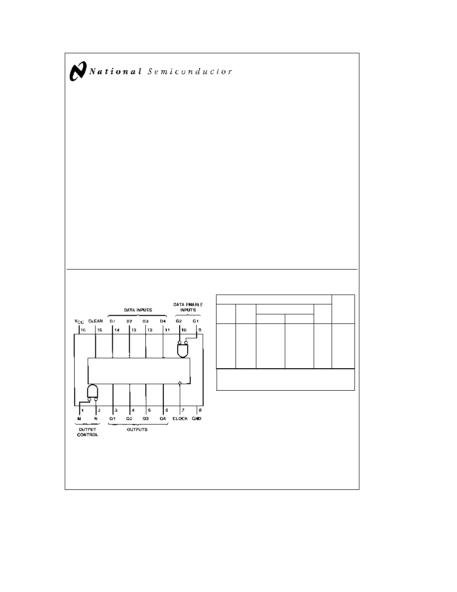
Connection Diagram
Dual-In-Line Package
TL F 6556 ≠ 1
Order Number 54173DMQB 54173FMQB
DM54173J DM54173W or DM74173N
See NS Package Number J16A N16E or W16A
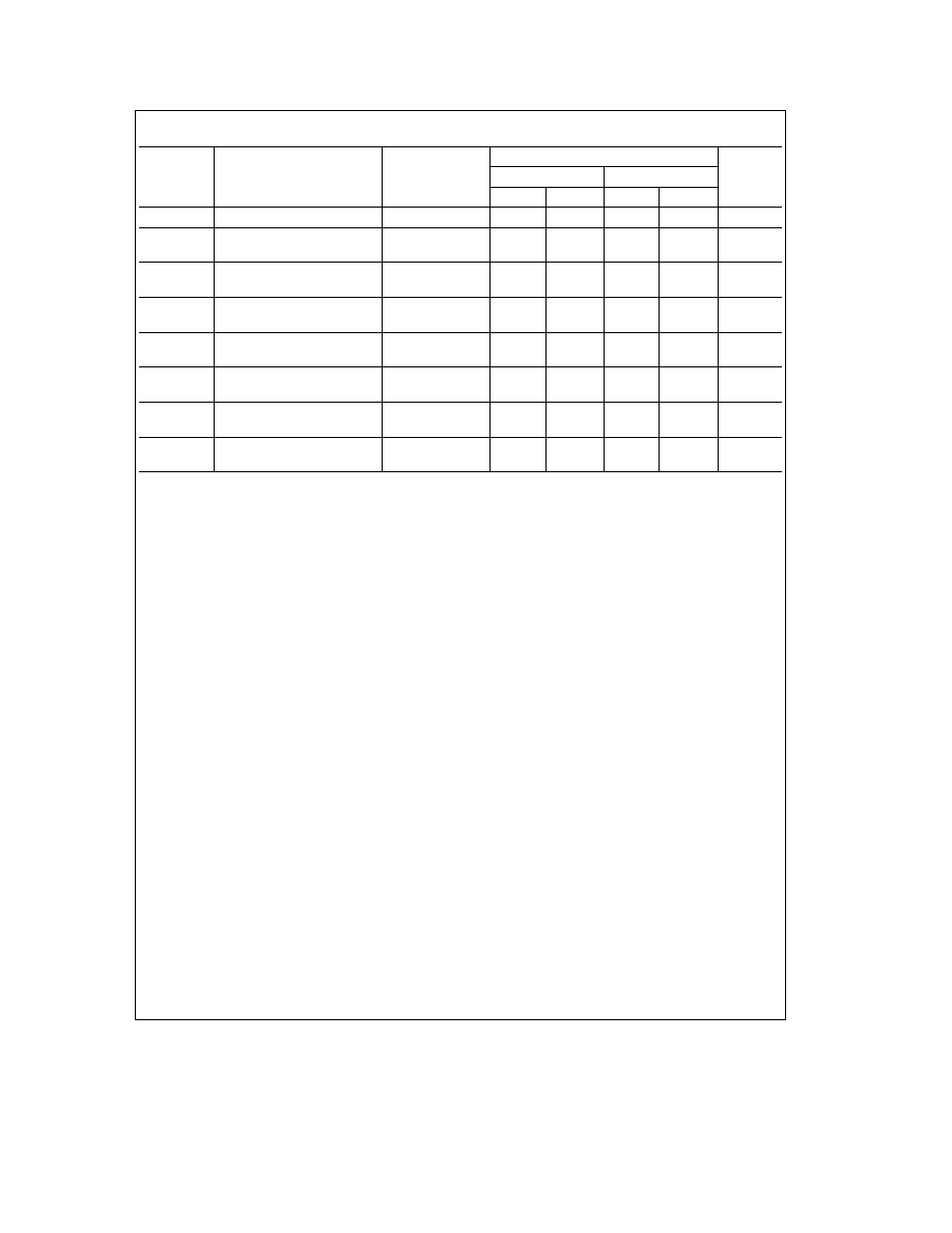
Function Table
Inputs
Output
Clear
Clock
Data Enable
Data
Q
G1
G2
D
H
X
X
X
X
L
L
L
X
X
X
Q
0
L
u
H
X
X
Q
0
L
u
X
H
X
Q
0
L
u
L
L
L
L
L
u
L
L
H
H
When either M or N (or both) is (are) high the output is disabled to the
high-impedance state however sequential operation of the flip-flops is
not affected
H
e
high level (steady state)
L
e
low level (steady state)
u
e
low-to-high level transition
X
e
don't care (any input including transitions)
Q
0
e
the level of Q before the indicated steady state input conditions were
established
TRI-STATE
is a registered trademark of National Semiconductor Corporation
C1995 National Semiconductor Corporation
RRD-B30M105 Printed in U S A
Absolute Maximum Ratings
(Note)
If Military Aerospace specified devices are required
please contact the National Semiconductor Sales
Office Distributors for availability and specifications
Supply Voltage
7V
Input Voltage
5 5V
Operating Free Air Temperature Range
DM54 and 54
b
55 C to
a
125 C
DM74
0 C to
a
70 C
Storage Temperature Range
b
65 C to
a
150 C
Note
The ``Absolute Maximum Ratings'' are those values
beyond which the safety of the device cannot be guaran-
teed The device should not be operated at these limits The
parametric values defined in the ``Electrical Characteristics''
table are not guaranteed at the absolute maximum ratings
The ``Recommended Operating Conditions'' table will define
the conditions for actual device operation
Recommended Operating Conditions
Symbol
Parameter
DM54173
DM74173
Units
Min
Nom
Max
Min
Nom
Max
V
CC
Supply Voltage
4 5
5
5 5
4 75
5
5 25
V
V
IH
High Level Input Voltage
2
2
V
V
IL
Low Level Input Voltage
0 8
0 8
V
I
OH
High Level Output Current
b
2
b
5 2
mA
I
OL
Low Level Output Current
16
16
mA
f
CLK
Clock Frequency (Note 4)
0
25
0
25
MHz
t
W
Pulse Width
Clock
20
20
ns
(Note 4)
Clear
20
20
t
SU
Setup Time
Enable
17
17
ns
(Note 4)
Data
10
10
t
H
Hold Time
Enable
2
2
ns
(Note 4)
Data
10
10
t
REL
Clear Release Time (Note 4)
10
10
ns
T
A
Free Air Operating Temperature
b
55
125
0
70
C
Electrical Characteristics
over recommended operating free air temperature range (unless otherwise noted)
Symbol
Parameter
Conditions
Min
Typ
Max
Units
(Note 1)
V
I
Input Clamp Voltage
V
CC
e
Min I
I
e b
12 mA
b
1 5
V
V
OH
High Level Output
V
CC
e
Min I
OH
e
Max
2 4
V
Voltage
V
IL
e
Max V
IH
e
Min
V
OL
Low Level Output
V
CC
e
Min I
OL
e
Max
0 4
V
Voltage
V
IH
e
Min V
IL
e
Max
I
I
Input Current
Max
V
CC
e
Max V
I
e
5 5V
1
mA
Input Voltage
I
IH
High Level Input Current
V
CC
e
Max V
I
e
2 4V
40
m
A
I
IL
Low Level Input Current
V
CC
e
Max V
I
e
0 4V
b
1 6
mA
I
OZH
Off-State Output Current with High
V
CC
e
Max V
O
e
2 4V
40
m
A
Level Output Voltage Applied
V
IH
e
Min V
IL
e
Max
I
OZL
Off-State Output Current with Low
V
CC
e
Max V
O
e
0 4V
b
40
m
A
Level Output Voltage Applied
V
IH
e
Min V
IL
e
Max
I
OS
Short Circuit
V
CC
e
Max
DM54
b
30
b
70
mA
Output Current
(Note 2)
DM74
b
30
b
70
I
CC
Supply Current
V
CC
e
Max (Note 3)
50
72
mA
Note 1
All typicals are at V
CC
e
5V T
A
e
25 C
Note 2
Not more than one output should be shorted at a time
Note 3
I
CC
is measured with all outputs open CLEAR grounded after a momentary connection to 4 5V N G1 G2 and all DATA inputs grounded and the CLOCK
input and M input at 4 5V
Note 4
T
A
e
25 C and V
CC
e
5V
2