 | –≠–ª–µ–∫—Ç—Ä–æ–Ω–Ω—ã–π –∫–æ–º–ø–æ–Ω–µ–Ω—Ç: 54175DMQB | –°–∫–∞—á–∞—Ç—å:  PDF PDF  ZIP ZIP |
TL F 6557
54174DM54174DM74174
54175DM54175DM74175
HexQuad
D
Flip-Flops
with
Clear
June 1989
54174 DM54174 DM74174 54175 DM54175 DM74175
Hex Quad D Flip-Flops with Clear
General Description
These positive-edge triggered flip-flops utilize TTL circuitry
to implement D-type flip-flop logic All have a direct clear
input and the quad (175) version features complementary
outputs from each flip-flop
Information at the D inputs meeting the setup and hold time
requirements is transferred to the Q outputs on the positive-
going edge of the clock pulse Clock triggering occurs at a
particular voltage level and is not directly related to the tran-
sition time of the positive-going pulse When the clock input
is at either the high or low level the D input signal has no
effect at the output
Features
Y
174 contains six flip-flops with single-rail outputs
Y
175 contains four flip-flops with double-rail outputs
Y
Buffered clock and direct clear inputs
Y
Individual data input to each flip-flop
Y
Applications include
Buffer storage registers
Shift registers
Pattern generators
Y
Typical clock frequency 40 MHz
Y
Typical power dissipation per flip-flop 38 mW
Y
Alternate Military Aerospace device (54174 54175) is
available Contact a National Semiconductor Sales Of-
fice Distributor for specifications
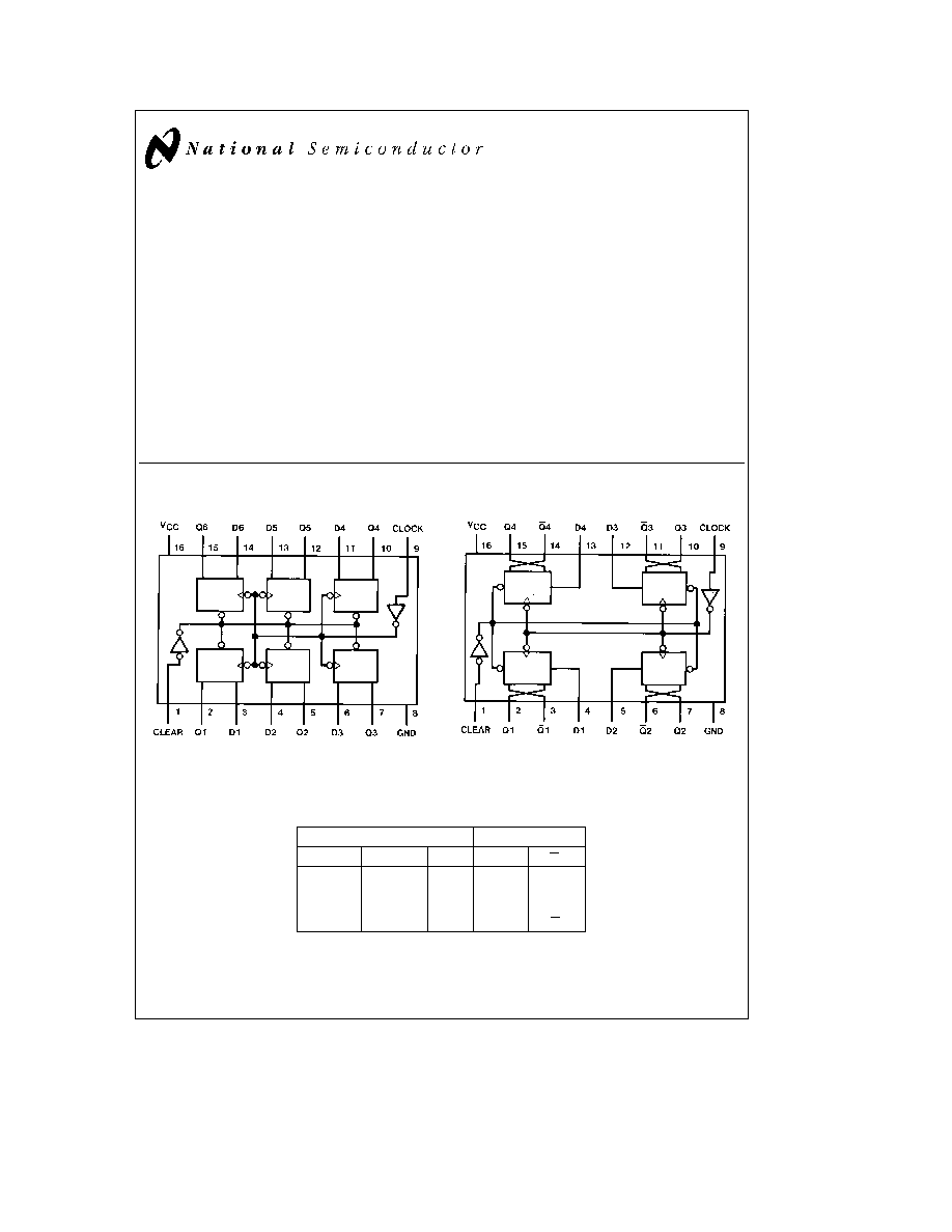
Connection Diagrams
Dual-In-Line Package
TL F 6557 ≠ 1
Order Number 54174DMQB 54174FMQB DM54174J
DM54174W or DM74174N
See NS Package Number J16A N16E or W16A
Dual-In-Line Package
TL F 6557 ≠ 2
Order Number 54175DMQB 54175FMQB DM54175J
DM54175W or DM74175N
See NS Package Number J16A N16E or W16A
Function Table
(Each Flip-Flop)
Inputs
Outputs
Clear
Clock
D
Q
Q
L
X
X
L
H
H
u
H
H
L
H
u
L
L
H
H
L
X
Q
0
Q
0
H
e
High Level (steady state)
L
e
Low Level (steady state)
X
e
Don't Care
u
e
Transition from low to high level
Q
0
e
The level of Q before the indicated steady-state input conditions were established
e
175 only
C1995 National Semiconductor Corporation
RRD-B30M105 Printed in U S A
Absolute Maximum Ratings
(Note)
If Military Aerospace specified devices are required
please contact the National Semiconductor Sales
Office Distributors for availability and specifications
Supply Voltage
7V
Input Voltage
5 5V
Operating Free Air Temperature Range
DM54 and 54
b
55 C to
a
125 C
DM74
0 C to
a
70 C
Storage Temperature Range
b
65 C to
a
150 C
Note
The ``Absolute Maximum Ratings'' are those values
beyond which the safety of the device cannot be guaran-
teed The device should not be operated at these limits The
parametric values defined in the ``Electrical Characteristics''
table are not guaranteed at the absolute maximum ratings
The ``Recommended Operating Conditions'' table will define
the conditions for actual device operation
Recommended Operating Conditions
Symbol
Parameter
DM54174
DM74174
Units
Min
Nom
Max
Min
Nom
Max
V
CC
Supply Voltage
4 5
5
5 5
4 75
5
5 25
V
V
IH
High Level Input Voltage
2
2
V
V
IL
Low Level Input Voltage
0 8
0 8
V
I
OH
High Level Output Current
b
0 8
b
0 8
mA
I
OL
Low Level Output Current
16
16
mA
f
CLK
Clock Frequency (Note 4)
0
30
0
30
MHz
t
W
Pulse Width
Clock Low
25
25
(Note 4)
Clock High
10
10
ns
Clear
20
20
t
SU
Data Setup Time (Note 4)
20
20
ns
t
H
Data Hold Time (Note 4)
0
0
ns
t
REL
Clear Release Time (Note 4)
30
30
ns
T
A
Free Air Operating Temperature
b
55
125
0
70
C
'174 Electrical Characteristics
over recommended operating free air temperature range (unless otherwise noted)
Symbol
Parameter
Conditions
Min
Typ
Max
Units
(Note 1)
V
I
Input Clamp Voltage
V
CC
e
Min I
I
e b
12 mA
b
1 5
V
V
OH
High Level Output
V
CC
e
Min I
OH
e
Max
2 4
V
Voltage
V
IL
e
Max V
IH
e
Min
V
OL
Low Level Output
V
CC
e
Min I
OL
e
Max
0 4
V
Voltage
V
IH
e
Min V
IL
e
Max
I
I
Input Current
Max
V
CC
e
Max V
I
e
5 5V
1
mA
Input Voltage
I
IH
High Level Input Current
V
CC
e
Max V
I
e
2 4V
40
m
A
I
IL
Low Level Input Current
V
CC
e
Max V
I
e
0 4V
b
1 6
mA
I
OS
Short Circuit
V
CC
e
Max
DM54
b
20
b
57
mA
Output Current
(Note 2)
DM74
b
18
b
57
I
CC
Supply Current
V
CC
e
Max (Note 3)
45
65
mA
Note 1
All typicals are at V
CC
e
5V T
A
e
25 C
Note 2
Not more than one output should be shorted at a time
Note 3
With all outputs open and all DATA and CLEAR inputs at 4 5V I
CC
is measured after a momentary ground then 4 5V applied to the CLOCK input
Note 4
T
A
e
25 C and V
CC
e
5V
2

'174 Switching Characteristics
at V
CC
e
5V and T
A
e
25 C (See Section 1 for Test Waveforms and Output Load)
Symbol
Parameter
From (Input)
R
L
e
400X C
L
e
15 pF
Units
To (Output)
Min
Max
f
MAX
Maximum Clock
30
MHz
Frequency
t
PLH
Propagation Delay Time
Clock to
25
ns
Low to High Level Output
Any Q
t
PHL
Propagation Delay Time
Clock to
25
ns
High to Low Level Output
Any Q
t
PHL
Propagation Delay Time
Clear to
40
ns
High to Low Level Output
Any Q
Recommended Operating Conditions
Symbol
Parameter
DM54175
DM74175
Units
Min
Nom
Max
Min
Nom
Max
V
CC
Supply Voltage
4 5
5
5 5
4 75
5
5 25
V
V
IH
High Level Input Voltage
2
2
V
V
IL
Low Level Input Voltage
0 8
0 8
V
I
OH
High Level Output Current
b
0 8
b
0 8
mA
I
OL
Low Level Output Current
16
16
mA
f
CLK
Clock Frequency (Note 1)
0
30
0
30
MHz
t
W
Pulse Width
Clock Low
25
25
(Note 1)
Clock High
10
10
ns
Clear
20
20
t
SU
Data Setup Time (Note 1)
20
20
ns
t
H
Data Hold Time (Note 1)
0
0
ns
t
REL
Clear Release Time (Note 1)
30
30
ns
T
A
Free Air Operating Temperature
b
55
125
0
70
C
Note 1
T
A
e
25 C and V
CC
e
5V
3
'175 Electrical Characteristics
over recommended operating free air temperature range (unless otherwise noted)
Symbol
Parameter
Conditions
Min
Typ
Max
Units
(Note 1)
V
I
Input Clamp Voltage
V
CC
e
Min I
I
e b
12 mA
b
1 5
V
V
OH
High Level Output
V
CC
e
Min I
OH
e
Max
2 4
V
Voltage
V
IL
e
Max V
IH
e
Min
V
OL
Low Level Output
V
CC
e
Min I
OL
e
Max
0 4
V
Voltage
V
IH
e
Min V
IL
e
Max
I
I
Input Current
Max
V
CC
e
Max V
I
e
5 5V
1
mA
Input Voltage
I
IH
High Level Input Current
V
CC
e
Max V
I
e
2 4V
40
m
A
I
IL
Low Level Input Current
V
CC
e
Max V
I
e
0 4V
b
1 6
mA
I
OS
Short Circuit
V
CC
e
Max
DM54
b
20
b
57
mA
Output Current
(Note 2)
DM74
b
18
b
57
I
CC
Supply Current
V
CC
e
Max (Note 3)
30
45
mA
'175 Switching Characteristics
at V
CC
e
5V and T
A
e
25 C (See Section 1 for Test Waveforms and Output Load)
Symbol
Parameter
From (Input)
R
L
e
400X C
L
e
15 pF
Units
To (Output)
Min
Max
f
MAX
Maximum Clock
30
MHz
Frequency
t
PLH
Propagation Delay Time
Clock to
25
ns
Low to High Level Output
Any Q or Q
t
PHL
Propagation Delay Time
Clock to
25
ns
High to Low Level Output
Any Q or Q
t
PLH
Propagation Delay Time
Clear to
25
ns
Low to High Level Output
Any Q
t
PHL
Propagation Delay Time
Clear to
40
ns
High to Low Level Output
Any Q
Note 1
All typicals are at V
CC
e
5V T
A
e
25 C
Note 2
Not more than one output should be shorted at a time
Note 3
With all outputs open and 4 5V applied to all DATA and CLEAR inputs I
CC
is measured after a momentary ground then 4 5V applied to the CLOCK
4
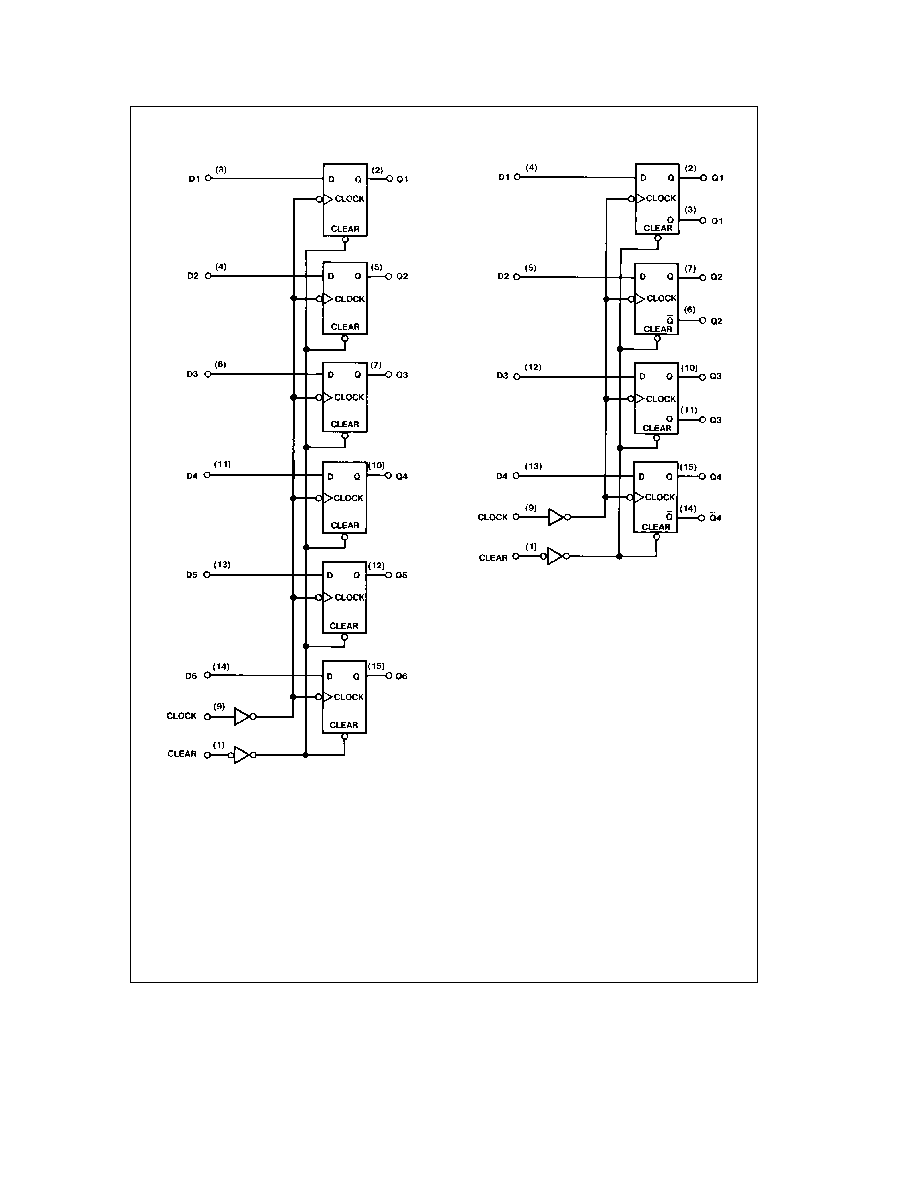
Logic Diagrams
174
TL F 6557 ≠ 3
175
TL F 6557 ≠ 4
5