TL F 6562
54191DM54191DM74191
Synchronous
UpDown
4-Bit
Binary
Counter
with
Mode
Control
June 1989
54191 DM54191 DM74191 Synchronous Up Down
4-Bit Binary Counter with Mode Control
General Description
This circuit is a synchronous reversible up down counter
The 191 is a 4-bit binary counter Synchronous operation is
provided by having all flip-flops clocked simultaneously so
that the outputs change simultaneously when so instructed
by the steering logic This mode of operation eliminates the
output counting spikes normally associated with asynchro-
nous (ripple clock) counters
The outputs of the four master-slave flip-flops are triggered
on a low-to-high level transition of the clock input if the
enable input is low A high at the enable input inhibits count-
ing Level changes at either the enable input or the down
up input should be made only when the clock input is high
The direction of the count is determined by the level of the
down up input When low the counter counts up and when
high it counts down
This counter is fully programmable that is the outputs may
be preset to either level by placing a low on the load input
and entering the desired data at the data inputs The output
will change independent of the level of the clock input This
feature allows the counters to be used as modulo-N dividers
by simply modifying the count length with the preset inputs
The clock down up and load inputs are buffered to lower
the drive requirement which significantly reduces the num-
ber of clock drivers etc required for long parallel words
Two outputs have been made available to perform the cas-
cading function ripple clock and maximum minimum count
The latter output produces a high-level output pulse with a
duration approximately equal to one complete cycle of the
clock when the counter overflows or underflows The ripple
clock output produces a low-level output pulse equal in
width to the low-level portion of the clock input when an
overflow or underflow condition exists The counters can be
easily cascaded by feeding the ripple clock output to the
enable input of the succeeding counter if parallel clocking is
used or to the clock input if parallel enabling is used The
maximum minimum count output can be used to accom-
plish look-ahead for high-speed operation
Features
Y
Single down up count control line
Y
Count enable control input
Y
Ripple clock output for cascading
Y
Asynchronously presettable with load control
Y
Parallel outputs
Y
Cascadable for n-bit applications
Y
Alternate Military Aerospace device (54191) is avail-
able Contact a National Semiconductor Sales Office
Distributor for specifications
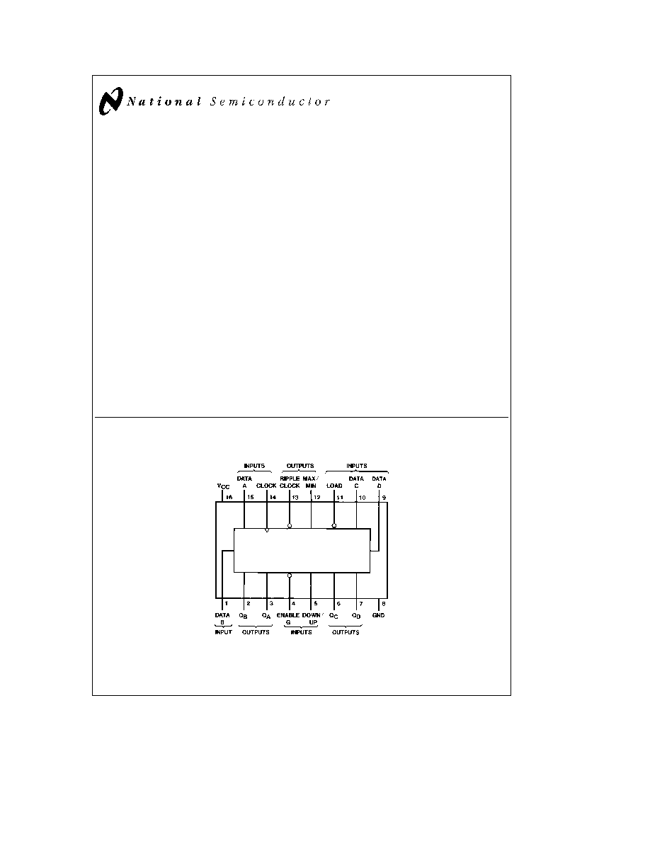
Connection Diagram
Dual-In-Line Package
TL F 6562 ≠ 1
Order Number 54191DMQB 54191FMQB
DM54191J DM54191W or DM74191N
See NS Package Number J16A N16E or W16A
C1995 National Semiconductor Corporation
RRD-B30M105 Printed in U S A
Absolute Maximum Ratings
(Note)
If Military Aerospace specified devices are required
please contact the National Semiconductor Sales
Office Distributors for availability and specifications
Supply Voltage
7V
Input Voltage
5 5V
Operating Free Air Temperature Range
DM54 and 54
b
55 C to
a
125 C
DM74
0 C to
a
70 C
Storage Temperature Range
b
65 C to
a
150 C
Note
The ``Absolute Maximum Ratings'' are those values
beyond which the safety of the device cannot be guaran-
teed The device should not be operated at these limits The
parametric values defined in the ``Electrical Characteristics''
table are not guaranteed at the absolute maximum ratings
The ``Recommended Operating Conditions'' table will define
the conditions for actual device operation
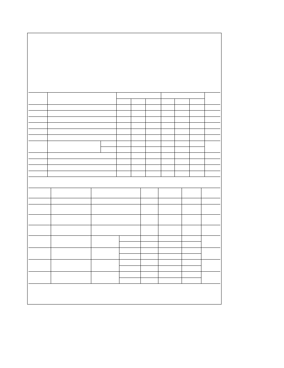
Recommended Operating Conditions
Symbol
Parameter
DM54191
DM74191
Units
Min
Nom
Max
Min
Nom
Max
V
CC
Supply Voltage
4 5
5
5 5
4 75
5
5 25
V
V
IH
High Level Input Voltage
2
2
V
V
IL
Low Level Input Voltage
0 8
0 8
V
I
OH
High Level Output Current
b
0 8
b
0 8
mA
I
OL
Low Level Output Current
16
16
mA
f
CLK
Clock Frequency (Note 4)
0
20
0
20
MHz
t
W
Pulse Width
Clock
25
25
ns
(Note 4)
Load
35
35
t
SU
Data Setup Time (Note 4)
28
28
ns
t
H
Hold Time (Note 4)
0
0
ns
t
REL
Load Release Time (Note 4)
30
30
ns
T
A
Free Air Operating Temperature
b
55
125
0
70
C
Electrical Characteristics
over recommended operating free air temperature range (unless otherwise noted)
Symbol
Parameter
Conditions
Min
Typ
Max
Units
(Note 1)
V
I
Input Clamp Voltage
V
CC
e
Min I
I
e b
12 mA
b
1 5
V
V
OH
High Level Output
V
CC
e
Min I
OH
e
Max
2 4
3 4
V
Voltage
V
IL
e
Max V
IH
e
Min
V
OL
Low Level Output
V
CC
e
Min I
OL
e
Max
0 2
0 4
V
Voltage
V
IH
e
Min V
IL
e
Max
I
I
Input Current
Max
V
CC
e
Max V
I
e
5 5V
1
mA
Input Voltage
I
IH
High Level Input
V
CC
e
Max
Enable
120
m
A
Current
V
I
e
2 4V
Others
40
I
IL
Low Level Input
V
CC
e
Max
Enable
b
4 8
mA
Current
V
I
e
0 4V
Others
b
1 6
I
OS
Short Circuit
V
CC
e
Max
DM54
b
20
b
65
mA
Output Current
(Note 2)
DM74
b
18
b
65
I
CC
Supply Current
V
CC
e
Max
DM54
65
99
mA
(Note 3)
DM74
65
105
Note 1
All typicals are at V
CC
e
5V T
A
e
25 C
Note 2
Not more than one output should be shorted at a time
Note 3
I
CC
is measured with all inputs grounded and all outputs open
Note 4
T
A
e
25 C and V
CC
e
5V
2
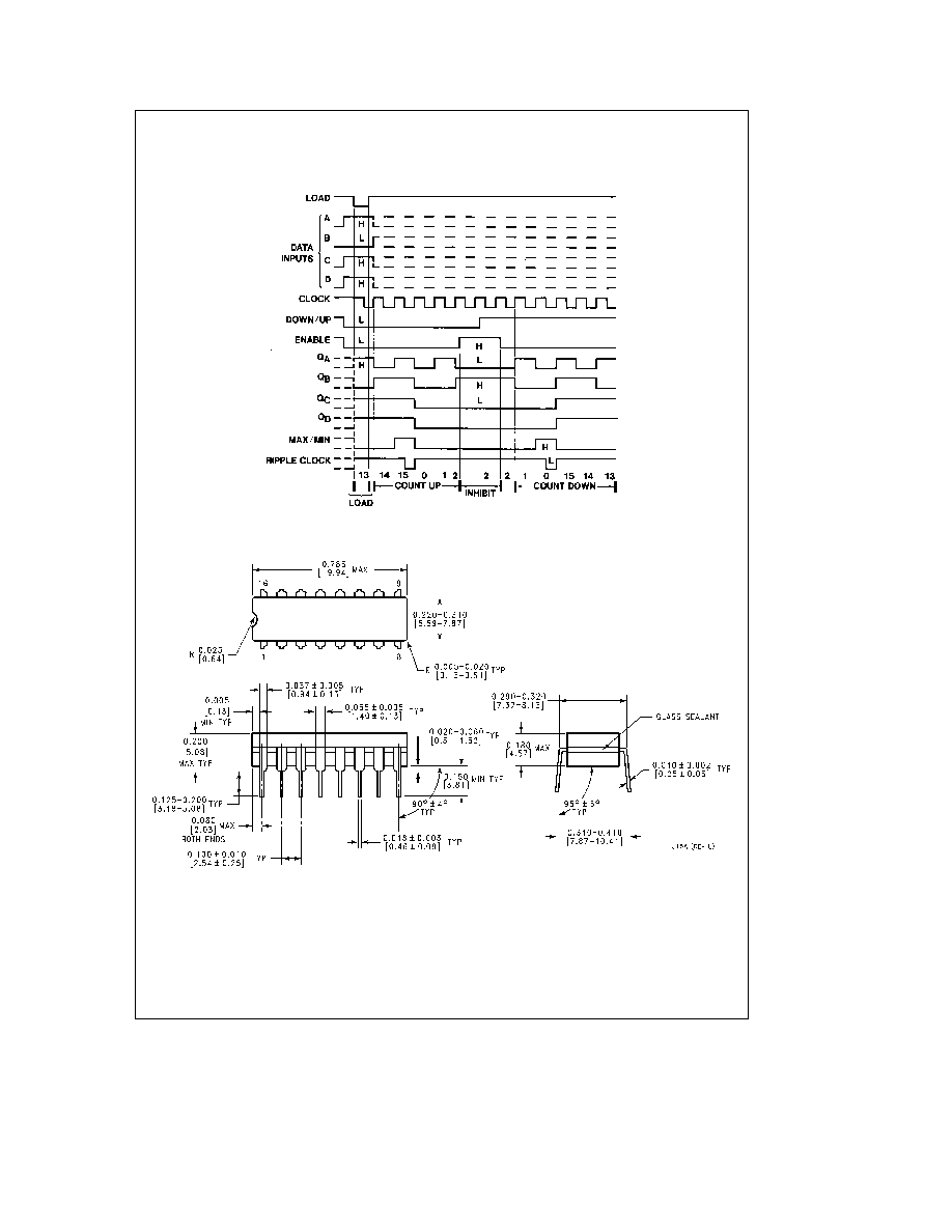
Timing Diagrams
191 Decade Counter
Typical Load Count and Inhibit Sequences
TL F 6562 ≠ 3
Physical Dimensions
inches (millimeters)
16-Lead Ceramic Dual-In-Line Package (J)
Order Number 54191DMQB or DM54191J
NS Package Number J16A
5

