 | –≠–ª–µ–∫—Ç—Ä–æ–Ω–Ω—ã–π –∫–æ–º–ø–æ–Ω–µ–Ω—Ç: 5442AFMQB | –°–∫–∞—á–∞—Ç—å:  PDF PDF  ZIP ZIP |
TL F 6516
5442ADM5442ADM7442A
BCD
to
Decimal
Decoders
June 1989
5442A DM5442A DM7442A
BCD to Decimal Decoders
General Description
These BCD-to-decimal decoders consist of eight inverters
and ten four-input NAND gates The inverters are connect-
ed in pairs to make BCD input data available for decoding
by the NAND gates Full decoding of input logic ensures
that all outputs remain off for all invalid (10 ≠ 15) input condi-
tions
Features
Y
Diode clamped inputs
Y
Also for application as 4-line-to-16-line decoders 3-line-
to-8-line decoders
Y
All outputs are high for invalid input conditions
Y
Typical power dissipation 140 mW
Y
Typical propagation delay 17 ns
Y
Alternate Military Aerospace device (5442A) is avail-
able Contact a National Semiconductor Sales Office
Distributor for specifications
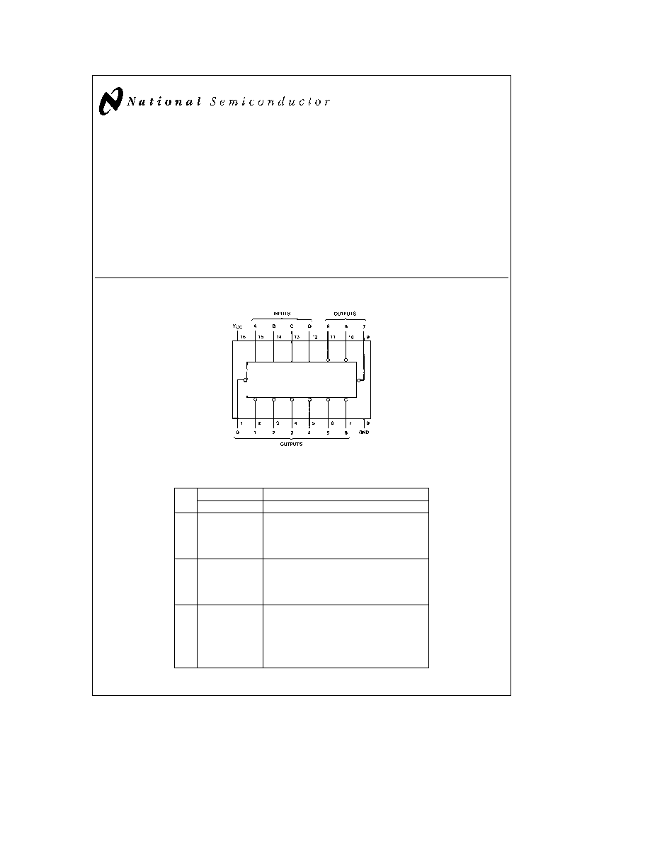
Connection Diagram
Dual-In-Line Package
TL F 6516 ≠ 1
Order Number 5442ADMQB 5442AFMQB DM5442AJ DM5442AW or DM7442AN
See NS Package Number J16A N16E or W16A
Function Table
No
BCD Input
Decimal Output
D
C
B
A
0
1
2
3
4
5
6
7
8
9
0
L
L
L
L
L
H
H
H
H
H
H
H
H
H
1
L
L
L
H
H
L
H
H
H
H
H
H
H
H
2
L
L
H
L
H
H
L
H
H
H
H
H
H
H
3
L
L
H
H
H
H
H
L
H
H
H
H
H
H
4
L
H
L
L
H
H
H
H
L
H
H
H
H
H
5
L
H
L
H
H
H
H
H
H
L
H
H
H
H
6
L
H
H
L
H
H
H
H
H
H
L
H
H
H
7
L
H
H
H
H
H
H
H
H
H
H
L
H
H
8
H
L
L
L
H
H
H
H
H
H
H
H
L
H
9
H
L
L
H
H
H
H
H
H
H
H
H
H
L
I
H
L
H
L
H
H
H
H
H
H
H
H
H
H
N
H
L
H
H
H
H
H
H
H
H
H
H
H
H
V
H
H
L
L
H
H
H
H
H
H
H
H
H
H
A
H
H
L
H
H
H
H
H
H
H
H
H
H
H
L
H
H
H
L
H
H
H
H
H
H
H
H
H
H
I
H
H
H
H
H
H
H
H
H
H
H
H
H
H
D
H
e
High Level
L
e
Low Level
C1995 National Semiconductor Corporation
RRD-B30M105 Printed in U S A
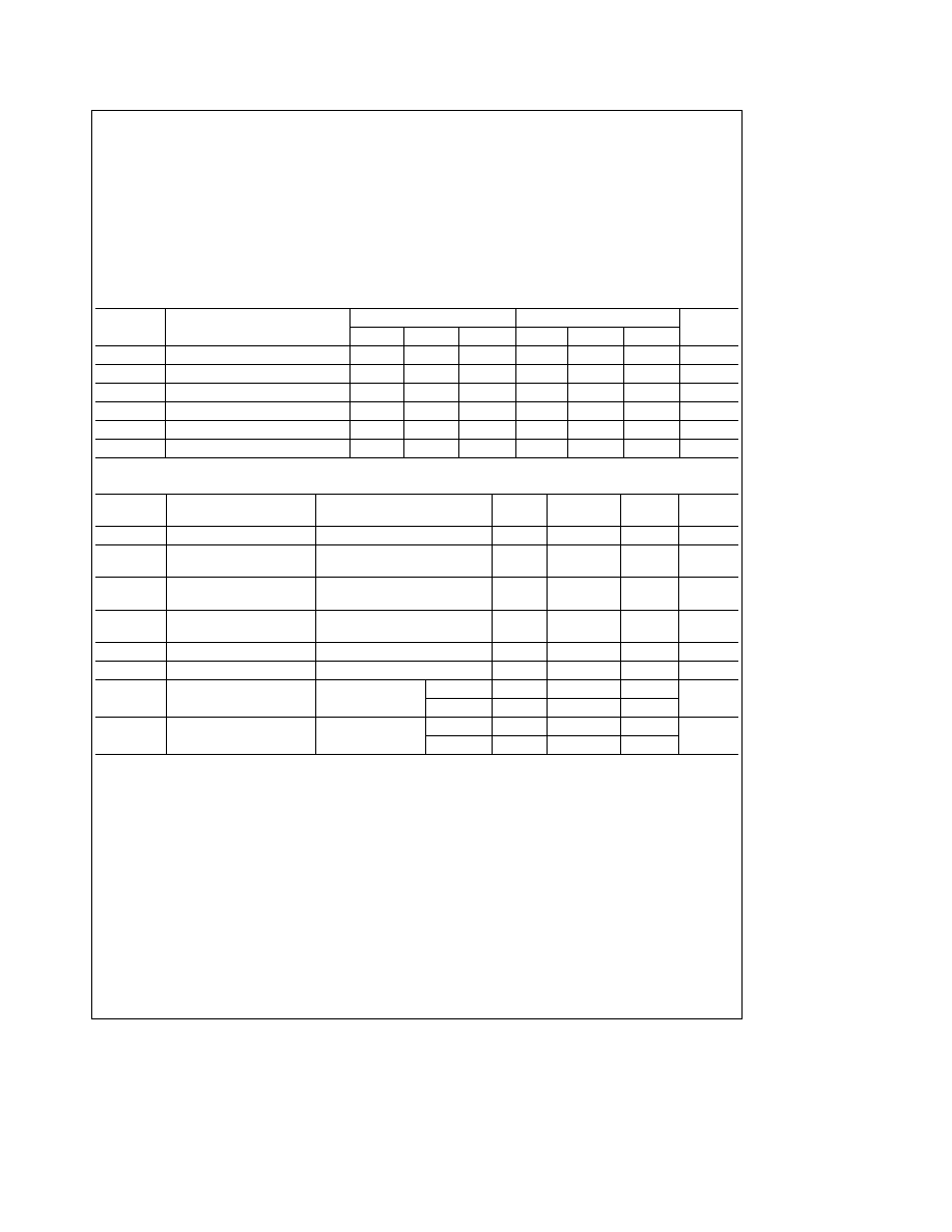
Absolute Maximum Ratings
(Note)
If Military Aerospace specified devices are required
please contact the National Semiconductor Sales
Office Distributors for availability and specifications
Supply Voltage
7V
Input Voltage
5 5V
Operating Free Air Temperature Range
DM54 and 54
b
55 C to
a
125 C
DM74
0 C to
a
70 C
Storage Temperature Range
b
65 C to
a
150 C
Note
The ``Absolute Maximum Ratings'' are those values
beyond which the safety of the device cannot be guaran-
teed The device should not be operated at these limits The
parametric values defined in the ``Electrical Characteristics''
table are not guaranteed at the absolute maximum ratings
The ``Recommended Operating Conditions'' table will define
the conditions for actual device operation
Recommended Operating Conditions
Symbol
Parameter
DM5442A
DM7442A
Units
Min
Nom
Max
Min
Nom
Max
V
CC
Supply Voltage
4 5
5
5 5
4 75
5
5 25
V
V
IH
High Level Input Voltage
2
2
V
V
IL
Low Level Input Voltage
0 8
0 8
V
I
OH
High Level Output Current
b
0 8
b
0 8
mA
I
OL
Low Level Output Current
16
16
mA
T
A
Free Air Operating Temperature
b
55
125
0
70
C
Electrical Characteristics
over recommended operating free air temperature range (unless otherwise noted)
Symbol
Parameter
Conditions
Min
Typ
Max
Units
(Note 1)
V
I
Input Clamp Voltage
V
CC
e
Min I
I
e b
12 mA
b
1 5
V
V
OH
High Level Output
V
CC
e
Min I
OH
e
Max
2 4
3 4
V
Voltage
V
IL
e
Max V
IH
e
Min
V
OL
Low Level Output
V
CC
e
Min I
OL
e
Max
0 2
0 4
V
Voltage
V
IH
e
Min V
IL
e
Max
I
I
Input Current
Max
V
CC
e
Max V
I
e
5 5V
1
mA
Input Voltage
I
IH
High Level Input Current
V
CC
e
Max V
I
e
2 4V
40
m
A
I
IL
Low Level Input Current
V
CC
e
Max V
I
e
0 4V
b
1 6
mA
I
OS
Short Circuit
V
CC
e
Max
DM54
b
20
b
55
mA
Output Current
(Note 2)
DM74
b
18
b
55
I
CC
Supply Current
V
CC
e
Max
DM54
28
41
mA
(Note 3)
DM74
28
56
Note 1
All typicals are at V
CC
e
5V T
A
e
25 C
Note 2
Not more than one output should be shorted at a time
Note 3
I
CC
is measured with all outputs open and all inputs grounded
2

Switching Characteristics
at V
CC
e
5V and T
A
e
25 C (See Section 1 for Test Waveforms and Output Load)
Symbol
Parameter
Conditions
Min
Max
Units
t
PHL
Propagation Delay Time
C
L
e
15 pF
High to Low Level Output
R
L
e
400X
25
ns
from A B C or D through
2 Levels of Logic
t
PHL
Propagation Delay Time
High to Low Level Output
30
ns
from A B C or D through
3 Levels of Logic
t
PLH
Propagation Delay Time
Low to High Level Output
25
ns
from A B C or D through
2 Levels of Logic
t
PLH
Propagation Delay Time
Low to High Level Output
30
ns
from A B C or D through
3 Levels of Logic
Logic Diagram
Tl F 6516 ≠ 2
3

4

Physical Dimensions
inches (millimeters)
16-Lead Ceramic Dual-In-Line Package (J)
Order Number 5442ADMQB or DM5442AJ
NS Package Number J16A
16-Lead Molded Dual-In-Line Package (N)
Order Number DM7442AN
NS Package Number N16E
5