 | –≠–ª–µ–∫—Ç—Ä–æ–Ω–Ω—ã–π –∫–æ–º–ø–æ–Ω–µ–Ω—Ç: 5474 | –°–∫–∞—á–∞—Ç—å:  PDF PDF  ZIP ZIP |
TL F 6526
5474DM5474DM7474
Dual
Positive-Edge-Triggered
D
Flip-Flops
with
Preset
Clear
and
Complementary
Outputs
June 1989
5474 DM5474 DM7474
Dual Positive-Edge-Triggered D Flip-Flops
with Preset Clear and Complementary Outputs
General Description
This device contains two independent positive-edge-trig-
gered D flip-flops with complementary outputs The informa-
tion on the D input is accepted by the flip-flops on the posi-
tive going edge of the clock pulse The triggering occurs at a
voltage level and is not directly related to the transition time
of the rising edge of the clock The data on the D input may
be changed while the clock is low or high without affecting
the outputs as long as the data setup and hold times are not
violated A low logic level on the preset or clear inputs will
set or reset the outputs regardless of the logic levels of the
other inputs
Features
Y
Alternate Military Aerospace device (5474) is available
Contact a National Semiconductor Sales Office Distrib-
utor for specifications
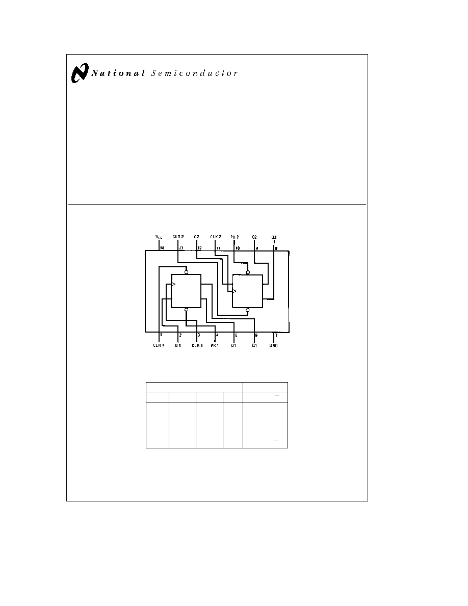
Connection Diagram
Dual-In-Line Package
TL F 6526 ≠ 1
Order Number 5474DMQB 5474FMQB DM5474J DM5474W DM7474M or DM7474N
See NS Package Number J14A M14A N14A or W14B
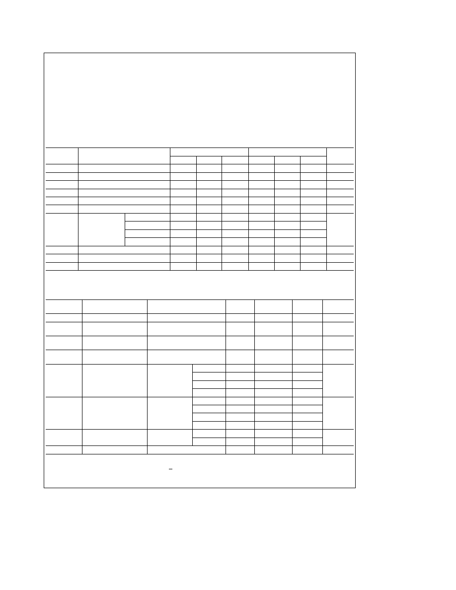
Function Table
Inputs
Outputs
PR
CLR
CLK
D
Q
Q
L
H
X
X
H
L
H
L
X
X
L
H
L
L
X
X
H
H
H
H
u
H
H
L
H
H
u
L
L
H
H
H
L
X
Q
0
Q
0
H
e
High Logic Level
X
e
Either Low or High Logic Level
L
e
Low Logic Level
u
e
Positive-going transition of the clock
e
This configuration is nonstable that is it will not persist when either the preset and or clear
inputs return to their inactive (high) level
Q
0
e
The output logic level of Q before the indicated input conditions were established
C1995 National Semiconductor Corporation
RRD-B30M105 Printed in U S A
Absolute Maximum Ratings
(Note)
If Military Aerospace specified devices are required
please contact the National Semiconductor Sales
Office Distributors for availability and specifications
Supply Voltage
7V
Input Voltage
5 5V
Operating Free Air Temperature Range
DM54 and 54
b
55 C to
a
125 C
DM74
0 C to
a
70 C
Storage Temperature Range
b
65 C to
a
150 C
Note
The ``Absolute Maximum Ratings'' are those values
beyond which the safety of the device cannot be guaran-
teed The device should not be operated at these limits The
parametric values defined in the ``Electrical Characteristics''
table are not guaranteed at the absolute maximum ratings
The ``Recommended Operating Conditions'' table will define
the conditions for actual device operation
Recommended Operating Conditions
Symbol
Parameter
DM5474
DM7474
Units
Min
Nom
Max
Min
Nom
Max
V
CC
Supply Voltage
4 5
5
5 5
4 75
5
5 25
V
V
IH
High Level Input Voltage
2
2
V
V
IL
Low Level Input Voltage
0 8
0 8
V
I
OH
High Level Output Current
b
0 4
b
0 4
mA
I
OL
Low Level Output Current
16
16
mA
f
CLK
Clock Frequency (Note 2)
0
15
0
15
MHz
t
W
Pulse Width
Clock High
30
30
(Note 2)
Clock Low
37
37
ns
Clear Low
30
30
Preset Low
30
30
t
SU
Input Setup Time (Notes 1
2)
20
u
20
u
ns
t
H
Input Hold Time (Notes 1
2)
5
u
5
u
ns
T
A
Free Air Operating Temperature
b
55
125
0
70
C
Note 1
The symbol (
u
) indicates the rising edge of the clock pulse is used for reference
Note 2
T
A
e
25 C and V
CC
e
5V
Electrical Characteristics
over recommended operating free air temperature range (unless otherwise noted)
Symbol
Parameter
Conditions
Min
Typ
Max
Units
(Note 3)
V
I
Input Clamp Voltage
V
CC
e
Min I
I
e b
12 mA
b
1 5
V
V
OH
High Level Output
V
CC
e
Min I
OH
e
Max
2 4
3 4
V
Voltage
V
IL
e
Max V
IH
e
Min
V
OL
Low Level Output
V
CC
e
Min I
OL
e
Max
0 2
0 4
V
Voltage
V
IH
e
Min V
IL
e
Max
I
I
Input Current
Max
V
CC
e
Max V
I
e
5 5V
1
mA
Input Voltage
I
IH
High Level Input
V
CC
e
Max
D
40
Current
V
I
e
2 4V
Clock
80
m
A
Clear
120
Preset
40
I
IL
Low Level Input
V
CC
e
Max
D
b
1 6
Current
V
I
e
0 4V
Clock
b
3 2
mA
(Note 6)
Clear
b
3 2
Preset
b
1 6
I
OS
Short Circuit
V
CC
e
Max
DM54
b
20
b
55
mA
Output Current
(Note 4)
DM74
b
18
b
55
I
CC
Supply Current
V
CC
e
Max (Note 5)
17
30
mA
Note 3
All typicals are at V
CC
e
5V T
A
e
25 C
Note 4
Not more than one output should be shorted at a time
Note 5
With all outputs open I
CC
is measured with the Q and Q outputs high in turn At the time of measurement the clock is grounded
Note 6
Clear is tested with preset high and preset is tested with clear high
2
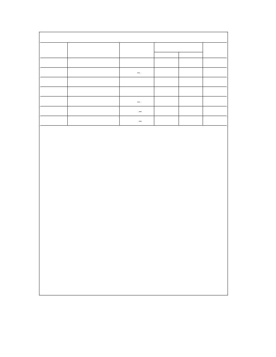
Switching Characteristics
at V
CC
e
5V and T
A
e
25 C (See Section 1 for Test Waveforms and Output Load)
From (Input)
R
L
e
400X
Symbol
Parameter
To (Output)
C
L
e
15 pF
Units
Min
Max
f
MAX
Maximum Clock
15
MHz
Frequency
t
PHL
Propagation Delay Time
Preset
40
ns
High to Low Level Output
to Q
t
PLH
Propagation Delay Time
Preset
25
ns
Low to High Level Output
to Q
t
PHL
Propagation Delay Time
Clear
40
ns
High to Low Level Output
to Q
t
PLH
Propagation Delay Time
Clear
25
ns
Low to High Level Output
to Q
t
PHL
Propagation Delay Time
Clock to
40
ns
High to Low Level Output
Q or Q
t
PLH
Propagation Delay Time
Clock to
25
ns
Low to High Level Output
Q or Q
3
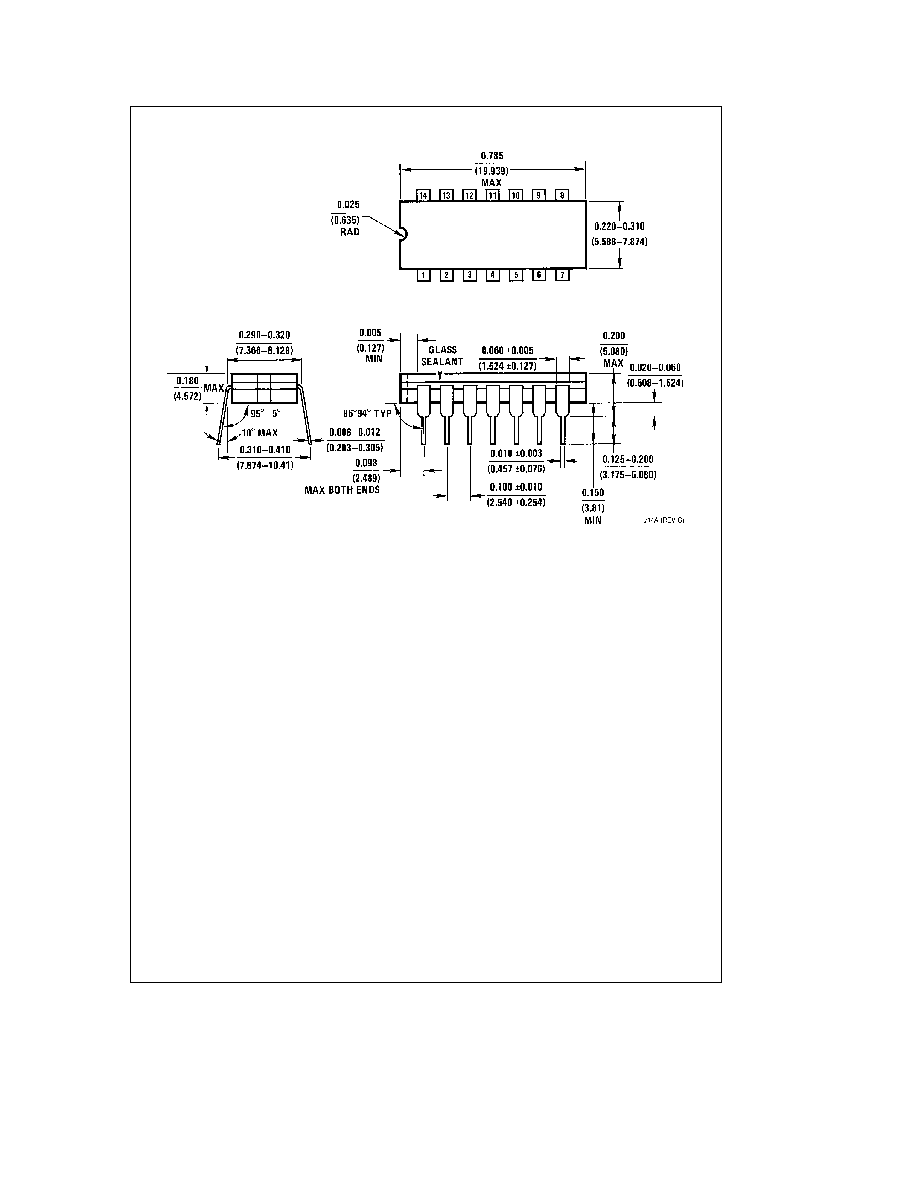
Physical Dimensions
inches (millimeters)
14-Lead Ceramic Dual-In-Line Package (J)
Order Number 5474DMQB or DM5474J
NS Package Number J14A
4
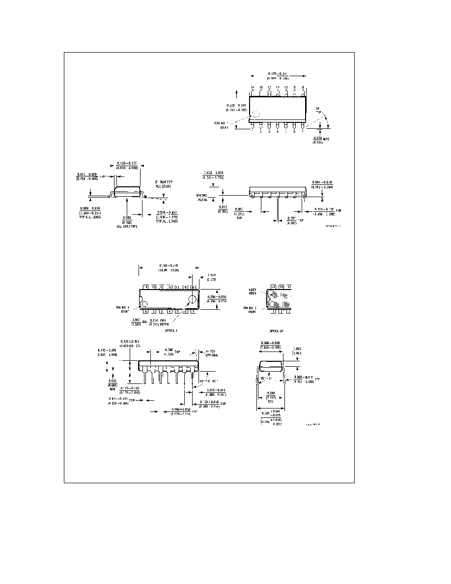
Physical Dimensions
inches (millimeters) (Continued)
14-Lead Small Outline Molded Package (M)
Order Number DM7474M
NS Package Number M14A
14-Lead Molded Dual-In-Line Package (N)
Order Number DM7474N
NS Package Number N14A
5