TL F 6531
5486DM5486DM7486
Quad
2-Input
Exclusive-OR
Gates
June 1989
5486 DM5486 DM7486
Quad 2-Input Exclusive-OR Gates
General Description
This device contains four independent gates each of which
performs the logic exclusive-OR function
Features
Y
Alternate Military Aerospace device (5486) is available
Contact a National Semiconductor Sales Office Distrib-
utor for specifications
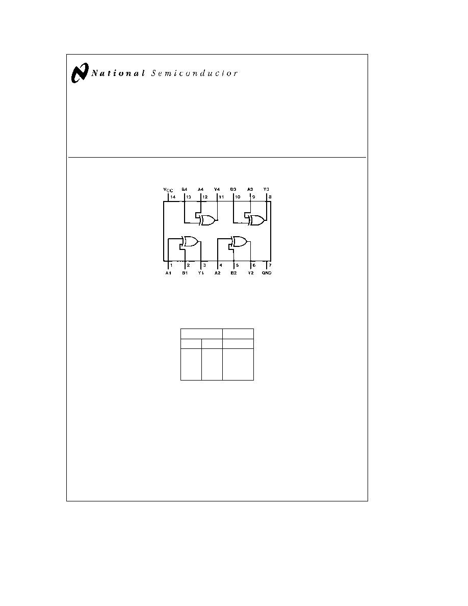
Connection Diagram
Dual-In-Line Package
TL F 6531 ≠ 1
Order Number 5486DMQB 5486FMQB DM5486J DM5486W or DM7486N
See NS Package Number J14A N14A or W14B
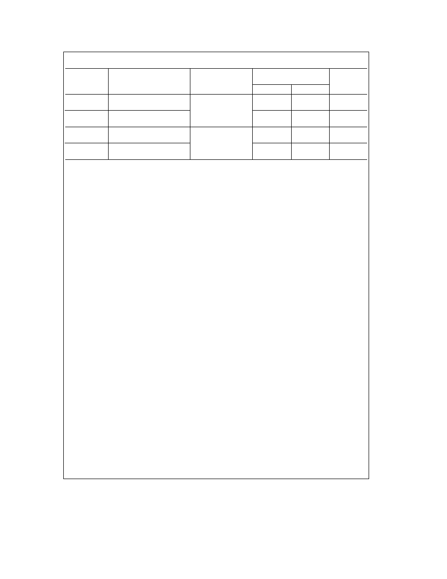
Function Table
Y
e
A
Z
B
Inputs
Output
A
B
Y
L
L
L
L
H
H
H
L
H
H
H
L
H
e
High Logic Level
L
e
Low Logic Level
C1995 National Semiconductor Corporation
RRD-B30M105 Printed in U S A
Absolute Maximum Ratings
(Note)
If Military Aerospace specified devices are required
please contact the National Semiconductor Sales
Office Distributors for availability and specifications
Supply Voltage
7V
Input Voltage
5 5V
Operating Free Air Temperature Range
DM54 and 54
b
55 C to
a
125 C
DM74
0 C to
a
70 C
Storage Temperature Range
b
65 C to
a
150 C
Note
The ``Absolute Maximum Ratings'' are those values
beyond which the safety of the device cannot be guaran-
teed The device should not be operated at these limits The
parametric values defined in the ``Electrical Characteristics''
table are not guaranteed at the absolute maximum ratings
The ``Recommended Operating Conditions'' table will define
the conditions for actual device operation
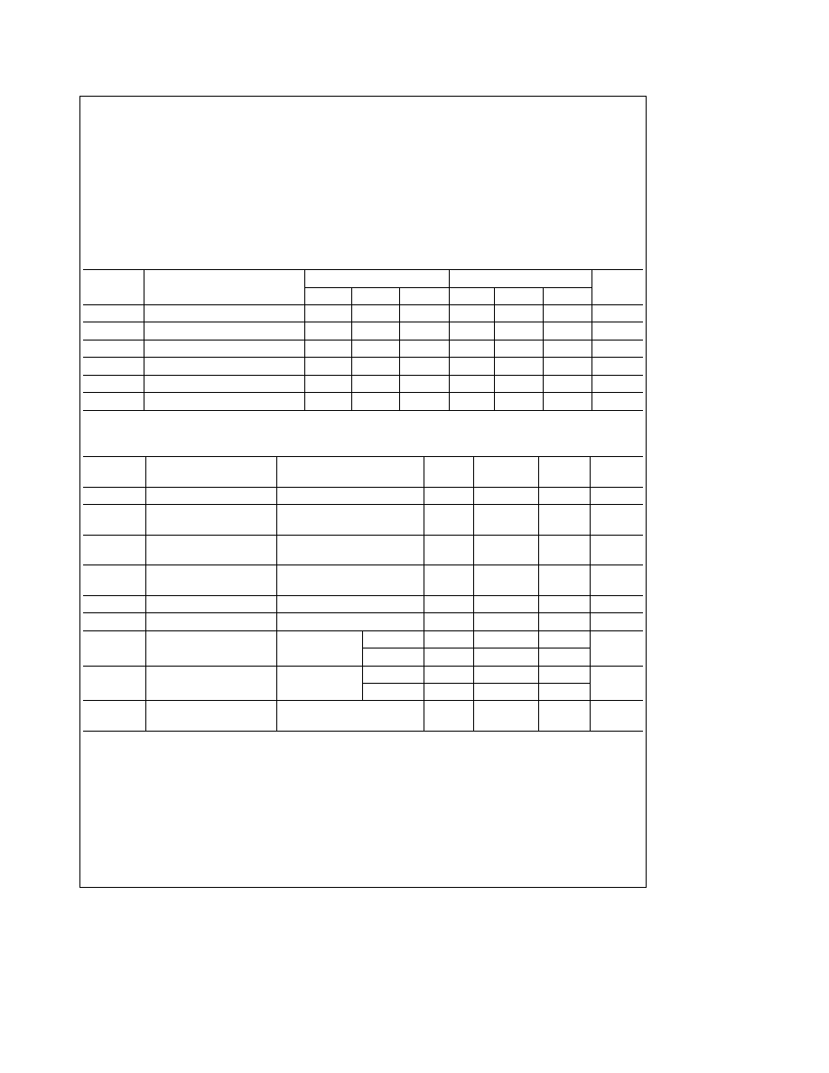
Recommended Operating Conditions
Symbol
Parameter
DM5486
DM7486
Units
Min
Nom
Max
Min
Nom
Max
V
CC
Supply Voltage
4 5
5
5 5
4 75
5
5 25
V
V
IH
High Level Input Voltage
2
2
V
V
IL
Low Level Input Voltage
0 8
0 8
V
I
OH
High Level Output Current
b
0 8
b
0 8
mA
I
OL
Low Level Output Current
16
16
mA
T
A
Free Air Operating Temperature
b
55
125
0
70
C
Electrical Characteristics
over recommended operating free air temperature range (unless otherwise noted)
Symbol
Parameter
Conditions
Min
Typ
Max
Units
(Note 1)
V
I
Input Clamp Voltage
V
CC
e
Min I
I
e b
12 mA
b
1 5
V
V
OH
High Level Output
V
CC
e
Min I
OH
e
Max
2 4
3 4
V
Voltage
V
IL
e
Max V
IH
e
Min
V
OL
Low Level Output
V
CC
e
Min I
OL
e
Max
0 2
0 4
V
Voltage
V
IH
e
Min V
IL
e
Max
I
I
Input Current
Max
V
CC
e
Max V
I
e
5 5V
1
mA
Input Voltage
I
IH
High Level Input Current
V
CC
e
Max V
I
e
2 4V
40
m
A
I
IL
Low Level Input Current
V
CC
e
Max V
I
e
0 4V
b
1 6
mA
I
OS
Short Circuit
V
CC
e
Max
DM54
b
20
b
55
mA
Output Current
(Note 2)
DM74
b
18
b
55
I
CCH
Supply Current with
V
CC
e
Max
DM54
30
43
mA
Outputs High
(Note 3)
DM74
30
50
I
CCL
Supply Current with
V
CC
e
Max (Note 4)
36
57
mA
Outputs Low
Note 1
All typicals are at V
CC
e
5V T
A
e
25 C
Note 2
Not more than one output should be shorted at a time
Note 3
I
CCH
is measured with all outputs open one input of each gate at 4 5V and the other inputs grounded
Note 4
I
CCL
is measured with all outputs open and all inputs at ground
2
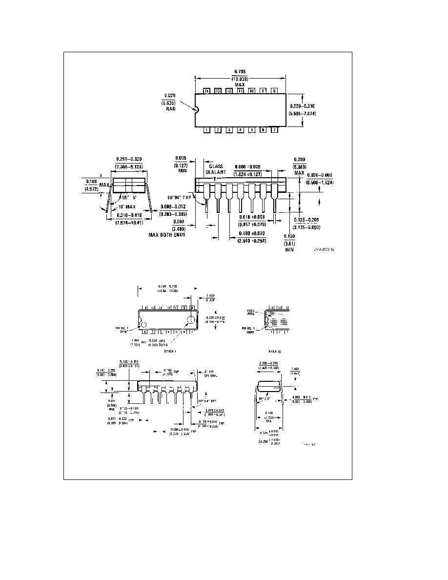
Physical Dimensions
inches (millimeters)
14-Lead Ceramic Dual-In-Line Package (J)
Order Number 5486DMQB or DM5486J
NS Package Number J14A
14-Lead Molded Dual-In-Line Package (N)
Order Number DM7486N
NS Package Number N14A
5