54ABT16373
16-Bit Transparent Latch with TRI-STATE
Æ
Outputs
General Description
The ABT16373 contains sixteen non-inverting latches with
TRI-STATE outputs and is intended for bus oriented applica-
tions. The device is byte controlled. The flip-flops appear
transparent to the data when the Latch Enable (LE) is HIGH.
When LE is low, the data that meets the setup time is
latched. Data appears on the bus when the Output Enable
(OE) is LOW. When OE is HIGH, the outputs are in high Z
state.
Features
n
Separate control logic for each byte
n
16-bit version of the ABT373
n
High impedance glitch free bus loading during entire
power up and power down cycle
n
Non-destructive hot insertion capability
n
Guaranteed latch-up protection
n
Standard Microcircuit Drawing (SMD) 5962-9320001
Ordering Code:
Military
Package
Package Description
Number
54ABT16373W-QML
WA48A
48-Lead Cerpack
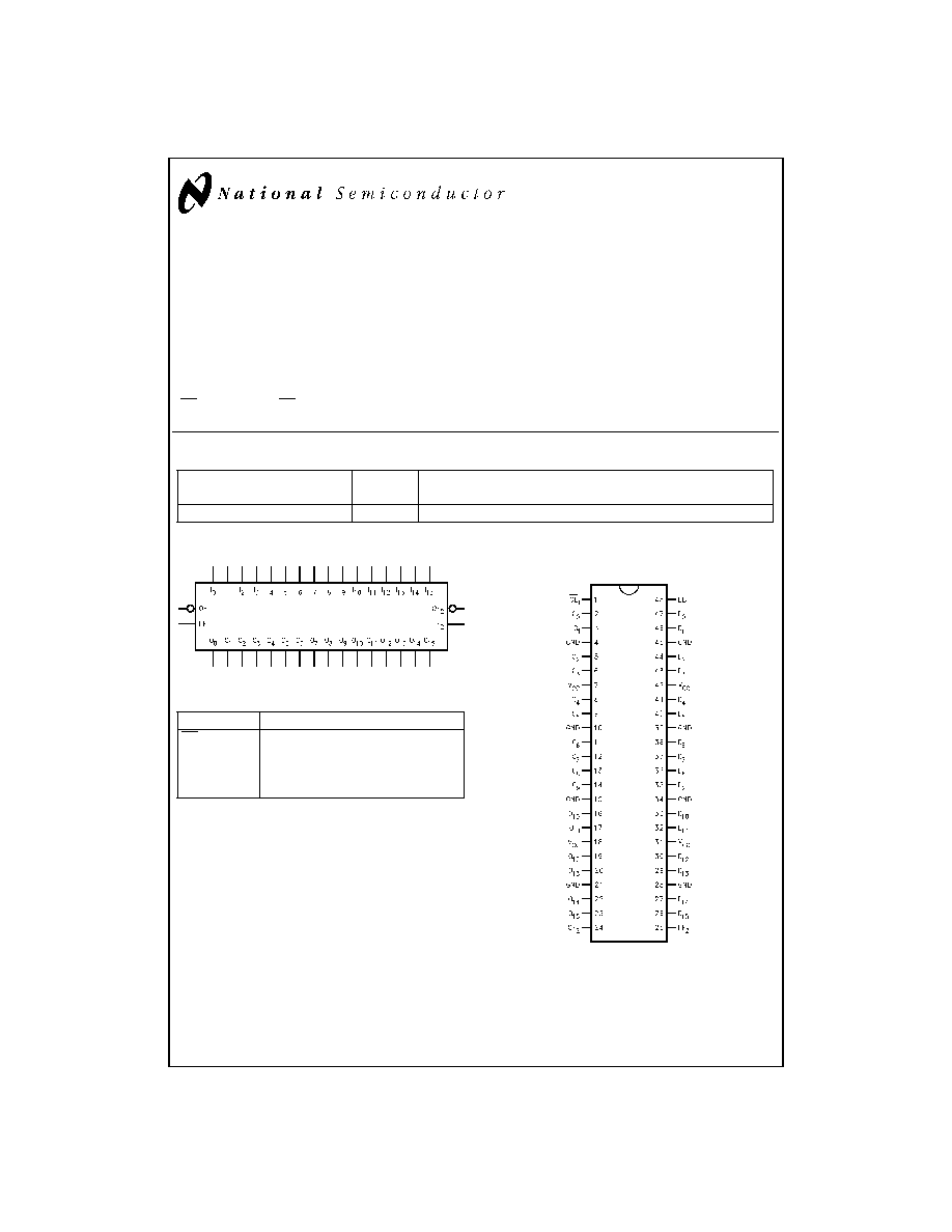
Logic Symbol
Pin Description
Pin Names
Description
OE
n
Output Enable Input (Active Low)
LE
n
Latch Enable Input
D
0
≠D
15
Data Inputs
O
0
≠O
15
Outputs
Connection Diagram
TRI-STATE
Æ
is a registered trademark of National Semiconductor Corporation.
DS100201-1
Pin Assignment for Cerpack
DS100201-2
July 1998
54ABT16373
16-Bit
T
ransparent
Latch
with
TRI-ST
A
T
E
Outputs
© 1998 National Semiconductor Corporation
DS100201
www.national.com
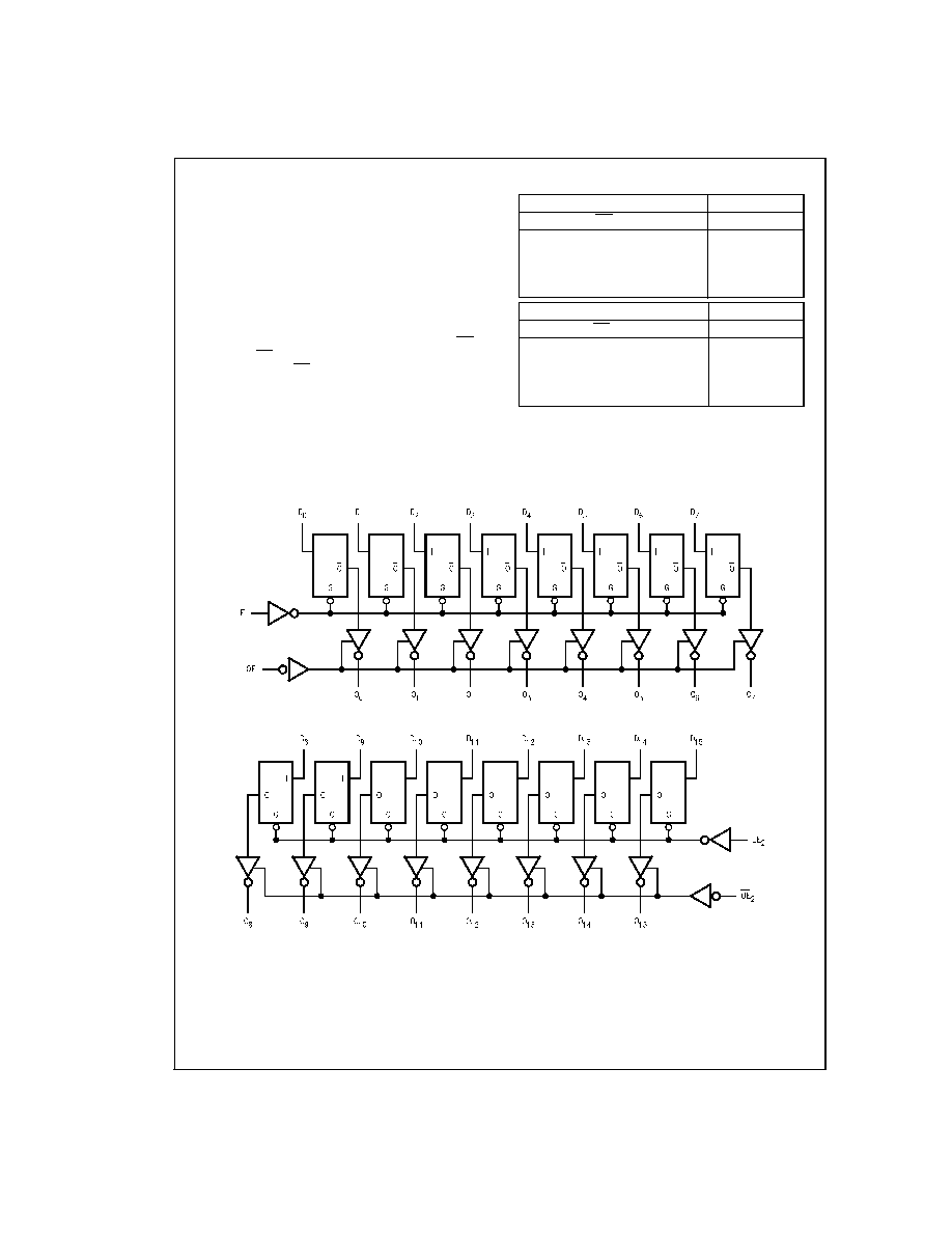
Functional Description
The ABT16373 contains sixteen D-type latches with
TRI-STATE standard outputs. The device is byte controlled
with each byte functioning identically, but independent of the
other. Control pins can be shorted together to obtain full
16-bit operation. The following description applies to each
byte. When the Latch Enable (LE
n
) input is HIGH, data on
the D
n
enters the latches. In this condition the latches are
transparent, i.e., a latch output will change states each time
its D input changes. When LE
n
is LOW, the latches store in-
formation that was present on the D inputs a setup time pre-
ceding the HIGH-to-LOW transition of LE
n
. The TRI-STATE
standard outputs are controlled by the Output Enable (OE
n
)
input. When OE
n
is LOW, the standard outputs are in the
2-state mode. When OE
n
is HIGH, the standard outputs are
in the high impedance mode but this does not interfere with
entering new data into the latches.
Truth Tables
Inputs
Outputs
LE
1
OE
1
D
0
≠D
7
O
0
≠O
7
X
H
X
Z
H
L
L
L
H
L
H
H
L
L
X
(Previous)
Inputs
Outputs
LE
2
OE
2
D
8
≠D
15
O
8
≠O
15
X
H
X
Z
H
L
L
L
H
L
H
H
L
L
X
(Previous)
H = High Voltage Level
L = Low Voltage Level
X = Immaterial
Z = High Impedance
Previous = previous output prior to HIGH to LOW transition of LE
Logic Diagrams
DS100201-3
DS100201-4
www.national.com
2
Absolute Maximum Ratings
(Note 1)
Storage Temperature
-65∞C to +150∞C
Ambient Temperature under Bias
-55∞C to +125∞C
Junction Temperature under Bias
Ceramic
-55∞C to +175∞C
V
CC
Pin Potential to
Ground Pin
-0.5V to +7.0V
Input Voltage (Note 2)
-0.5V to +7.0V
Input Current (Note 2)
-30 mA to +5.0 mA
Voltage Applied to Any Output
in the Disabled or
Power-Off State
-0.5V to +5.5V
in the HIGH State
-0.5V to V
CC
Current Applied to Output
in LOW State (Max)
twice the rated I
OL
(mA)
DC Latchup Source Current: OE Pin
-350 mA
(Across Comm Operating Range) Other Pins
-500 mA
Over Voltage Latchup (I/O)
10V
Recommended Operating
Conditions
Free Air Ambient Temperature
Military
-55∞C to +125∞C
Supply Voltage
Military
+4.5V to +5.5V
Minimum Input Edge Rate
(
V/
t)
Data Input
50 mV/ns
Enable Input
20 mV/ns
Note 1: Absolute maximum ratings are values beyond which the device may
be damaged or have its useful life impaired. Functional operation under these
conditions is not implied.
Note 2: Either voltage limit or current limit is sufficient to protect inputs.
DC Electrical Characteristics
Symbol
Parameter
ABT16373
Units
V
CC
Conditions
Min Typ
Max
V
IH
Input HIGH Voltage
2.0
V
Recognized HIGH Signal
V
IL
Input LOW Voltage
0.8
V
Recognized LOW Signal
V
CD
Input Clamp Diode Voltage
-1.2
V
Min
I
IN
= -18 mA
V
OH
Output HIGH Voltage
54ABT
2.5
I
OH
= -3 mA
54ABT
2.0
I
OH
= -24 mA
V
OL
Output LOW Voltage
54ABT
0.55
V
Min
I
OL
= 48 mA
I
IH
Input HIGH Current
5
µA
Max
V
IN
= 2.7V (Note 4)
5
V
IN
= V
CC
I
BVI
Input HIGH Current Breakdown Test
7
µA
Max
V
IN
= 7.0V
I
IL
Input LOW Current
-5
µA
Max
V
IN
= 0.5V (Note 4)
-5
V
IN
= 0.0V
V
ID
Input Leakage Test
4.75
V
0.0
I
ID
= 1.9 µA
All Other Pins Grounded
I
OZH
Output Leakage Current
50
µA
0 - 5.5V
V
OUT
= 2.7V; OE = 2.0V
I
OZL
Output Leakage Current
-50
µA
0 - 5.5V
V
OUT
= 0.5V; OE = 2.0V
I
OS
Output Short-Circuit Current
-100
-275
mA
Max
V
OUT
= 0.0V
I
CEX
Output High Leakage Current
50
µA
Max
V
OUT
= V
CC
I
ZZ
Bus Drainage Test
100
µA
0.0
V
OUT
= 5.5V; All Others GND
I
CCH
Power Supply Current
2.0
mA
Max
All Outputs HIGH
I
CCL
Power Supply Current
85
mA
Max
All Outputs LOW
I
CCZ
Power Supply Current
2.0
mA
Max
OE = V
CC
All Others at V
CC
or GND
I
CCT
Additional I
CC
/Input
Outputs Enabled
2.5
mA
V
I
= V
CC
- 2.1V
Outputs TRI-STATE
2.5
mA
Max
Enable Input V
I
= V
CC
- 2.1V
Outputs TRI-STATE
2.5
mA
Data Input V
I
= V
CC
- 2.1V
All Others at V
CC
or GND
I
CCD
Dynamic I
CC
No Load
mA/
Max
Outputs Open, LE = V
CC
(Note 4)
0.15
MHz
OE = GND, (Note 3)
One Bit Toggling, 50% Duty
Cycle
Note 3: For 8 bits toggling, I
CCD
<
0.8 mA/MHz.
Note 4: Guaranteed, but not tested.
3
www.national.com
AC Electrical Characteristics
Symbol
Parameter
54ABT
Units
T
A
= -55∞C to +125∞C
V
CC
= 4.5V to 5.5V
C
L
= 50 pF
Min
Max
t
PLH
Propagation Delay
1.4
6.5
ns
t
PHL
D
n
to O
n
1.4
6.5
t
PLH
Propagation Delay
1.7
7.0
ns
t
PHL
LE to O
n
1.4
6.3
t
PZH
Output Enable Time
1.1
6.8
ns
t
PZL
1.5
6.8
t
PHZ
Output Disable Time
1.5
8.5
ns
t
PLZ
1.6
8.0
AC Operating Requirements
Symbol
Parameter
54ABT
Units
T
A
= -55∞C to +125∞C
V
CC
= 4.5V to 5.5V
C
L
= 50 pF
Min
Max
t
s
(H)
Setup Time, HIGH
2.4
ns
t
s
(L)
or LOW D
n
to LE
2.4
t
h
(H)
Hold Time, HIGH
2.2
ns
t
h
(L)
or LOW D
n
to LE
2.2
t
w
(H)
Pulse Width,
3.3
ns
LE HIGH
Capacitance
Symbol
Parameter
Typ
Units
Conditions
(T
A
= 25∞C)
C
IN
Input Capacitance
5
pF
V
CC
= 0V
C
OUT
(Note 5)
Output Capacitance
11
pF
V
CC
= 5.0V
Note 5: C
OUT
is measured at frequency f = 1 MHz, per MIL-STD-883B, Method 3012.
www.national.com
4
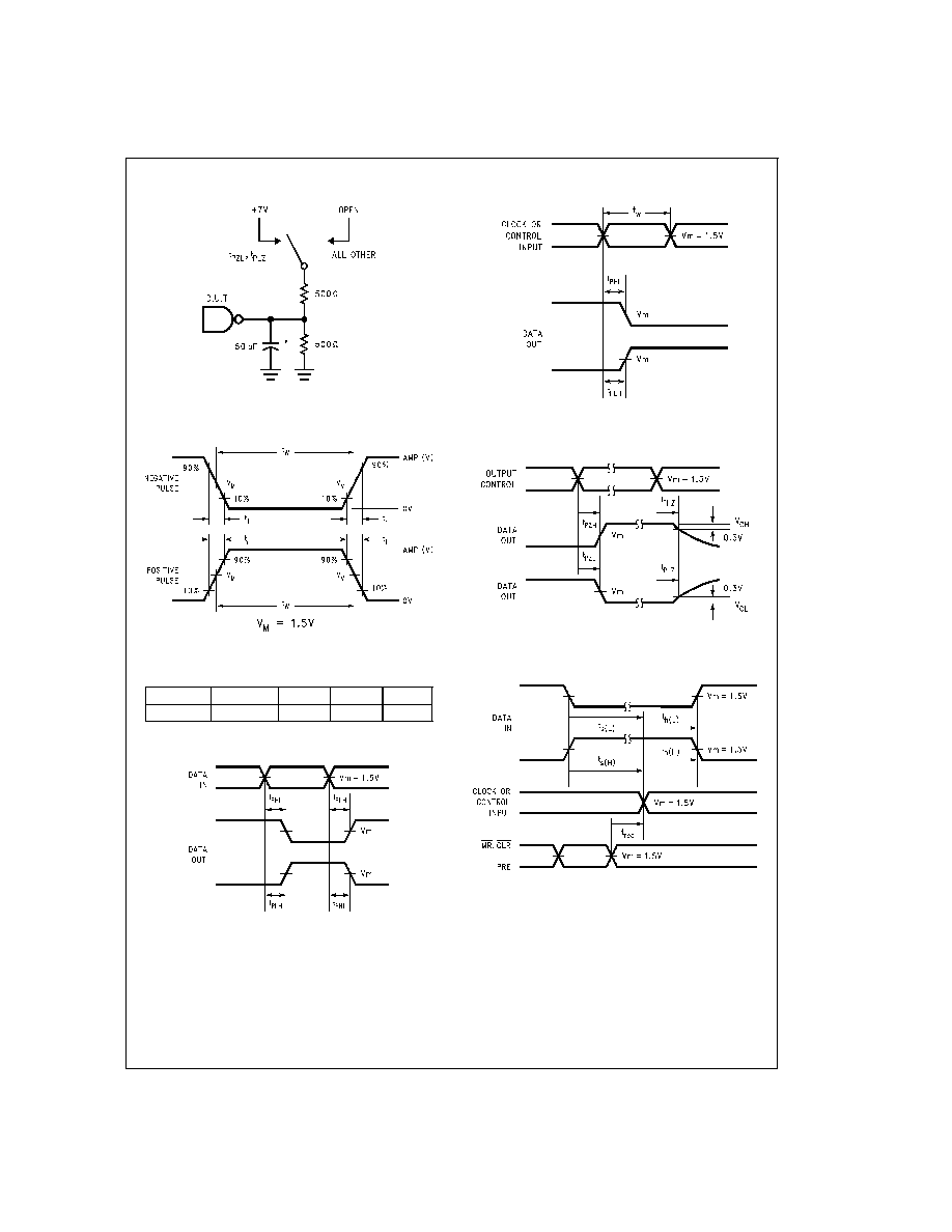
AC Loading
DS100201-6
*
Includes jig and probe capacitance
FIGURE 1. Standard AC Test Load
DS100201-10
FIGURE 2. Test Input Signal Levels
Amplitude
Rep. Rate
t
w
t
r
t
f
3.0V
1 MHz
500 ns
2.5 ns
2.5 ns
FIGURE 3. Test Input Signal Requirements
DS100201-8
FIGURE 4. Propagation Delay Waveforms for
Inverting and Non-Inverting Functions
DS100201-11
FIGURE 5. Propagation Delay,
Pulse Width Waveforms
DS100201-7
FIGURE 6. TRI-STATE Output HIGH
and LOW Enable and Disable Times
DS100201-9
FIGURE 7. Setup Time, Hold Time
and Recovery Time Waveforms
5
www.national.com