
54ABT652
Octal Transceivers and Registers with TRI-STATE
Æ
Outputs
General Description
The 'ABT652 consists of bus transceiver circuits with D-type
flip-flops, and control circuitry arranged for multiplexed trans-
mission of data directly from the input bus or from the inter-
nal registers. Data on the A or B bus will be clocked into the
registers as the appropriate clock pin goes to HIGH logic
level. Output Enable pins (OEAB, OEBA) are provided to
control the transceiver function.
Features
n
Independent registers for A and B buses
n
Multiplexed real-time and stored data
n
A and B output sink capability of 48 mA, source
capability of 24 mA
n
Guaranteed latchup protection
n
High impedance glitch free bus loading during entire
power up and power down cycle
n
Nondestructive hot insertion capability
n
Standard Microcircuit Drawing (SMD) 5962-9324201
Ordering Code:
Commercial
Package
Package Description
Number
54ABT652J-QML
J24A
24-Lead Ceramic Dual-in-line
54ABT652W-QML
W24C
24-Lead Cerpack
54ABT652E-QML
E28A
28-Lead Ceramic Leadless Chip Carrier, Type C
Connection Diagram
TRI-STATE
Æ
is a registered trademark of National Semiconductor Corporation.
Pin Assignment for
DIP and Flatpack
DS100220-1
August 1998
54ABT652
Octal
T
ransceivers
and
Registers
with
TRI-ST
A
T
E
Outputs
© 1998 National Semiconductor Corporation
DS100220
www.national.com

Connection Diagram
(Continued)
Pin Assignment for LCC
DS100220-48
www.national.com
2

Pin Descriptions
Pin Names
Description
A
0
≠A
7
Data Register A Inputs/TRI-STATE Outputs
B
0
≠B
7
Data Register B Inputs/TRI-STATE Outputs
CPAB, CPBA
Clock Pulse Inputs
SAB, SBA
Select Inputs
OEAB, OEBA
Output Enable Inputs
Logic Diagram
Functional Description
In the transceiver mode, data present at the HIGH imped-
ance port may be stored in either the A or B register or both.
The select (SAB, SBA) controls can multiplex stored and
real-time.
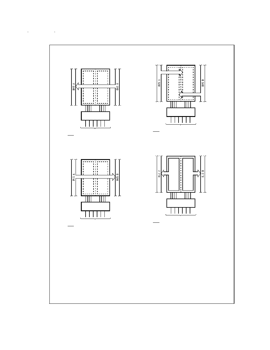
The examples in
Figure 1 demonstrate the four fundamental
bus-management functions that can be performed with the
'ABT652C.
Data on the A or B data bus, or both can be stored in the in-
ternal D flip-flop by LOW to HIGH transitions at the appropri-
ate Clock Inputs (CPAB, CPBA) regardless of the Select or
Output Enable Inputs. When SAB and SBA are in the real
time transfer mode, it is also possible to store data without
using the internal D flip-flops by simultaneously enabling
OEAB and OEBA. In this configuration each Output rein-
forces its Input. Thus when all other data sources to the two
sets of bus lines are in a HIGH impedance state, each set of
bus lines will remain at its last state.
DS100220-3
Please note that this diagram is provided only for the understanding of logic operations and should not be used to estimate propagation delays.
3
www.national.com
Functional Description
(Continued)
Note A: Real-Time
Transfer Bus B to Bus A
DS100220-4
OEAB
OEBA
CPAB
CPBA
SAB
SBA
L
L
X
X
X
L
Note C: Storage
DS100220-6
OEAB
OEBA
CPAB
CPBA
SAB
SBA
X
H
N
X
X
X
L
X
X
N
X
X
L
H
N
N
X
X
Note B: Real-Time
Transfer Bus A to Bus B
DS100220-5
OEAB
OEBA
CPAB
CPBA
SAB
SBA
H
H
X
X
L
X
Note D: Transfer Storage
Data to A or B
DS100220-7
OEAB
OEBA
CPAB
CPBA
SAB
SBA
H
L
H or L
H or L
H
H
FIGURE 1.
www.national.com
4

Functional Description
(Continued)
Inputs
Inputs/Outputs (Note 1)
Operating Mode
OEAB
OEBA
CPAB
CPBA
SAB
SBA
A
0
thru A
7
B
0
thru B
7
L
H
H or L
H or L
X
X
Input
Input
Isolation
L
H
N
N
X
X
Store A and B Data
X
H
N
H or L
X
X
Input
Not Specified
Store A, Hold B
H
H
N
N
X
X
Input
Output
Store A in Both Registers
L
X
H or L
N
X
X
Not Specified
Input
Hold A, Store B
L
L
N
N
X
X
Output
Input
Store B in Both Registers
L
L
X
X
X
L
Output
Input
Real-Time B Data to A Bus
L
L
X
H or L
X
H
Store B Data to A Bus
H
H
X
X
L
X
Input
Output
Real-Time A Data to B Bus
H
H
H or L
X
H
X
Stored A Data to B Bus
H
L
H or L
H or L
H
H
Output
Output
Stored A Data to B Bus and
Stored B Data to A Bus
H = HIGH Voltage Level
L = LOW Voltage Level
X = Immaterial
N = LOW to HIGH Clock Transition
Note 1: The data output functions may be enabled or disabled by various signals at OEAB or OEBA inputs. Data input functions are always enabled, i.e., data at
the bus pins will be stored on every LOW to HIGH transition on the clock inputs.
5
www.national.com