
TL F 10692
54AC74AC125
74ACT125
Quad
Buffer
with
TRI-STATE
Outputs
March 1993
54AC 74AC125
74ACT125
Quad Buffer with TRI-STATE
Outputs
General Description
The 'AC 'ACT125 contains four independent non-inverting
buffers with TRI-STATE outputs
Features
Y
I
CC
reduced by 50%
Y
Outputs source sink 24 mA
Y
'ACT125 has TTL-compatible outputs
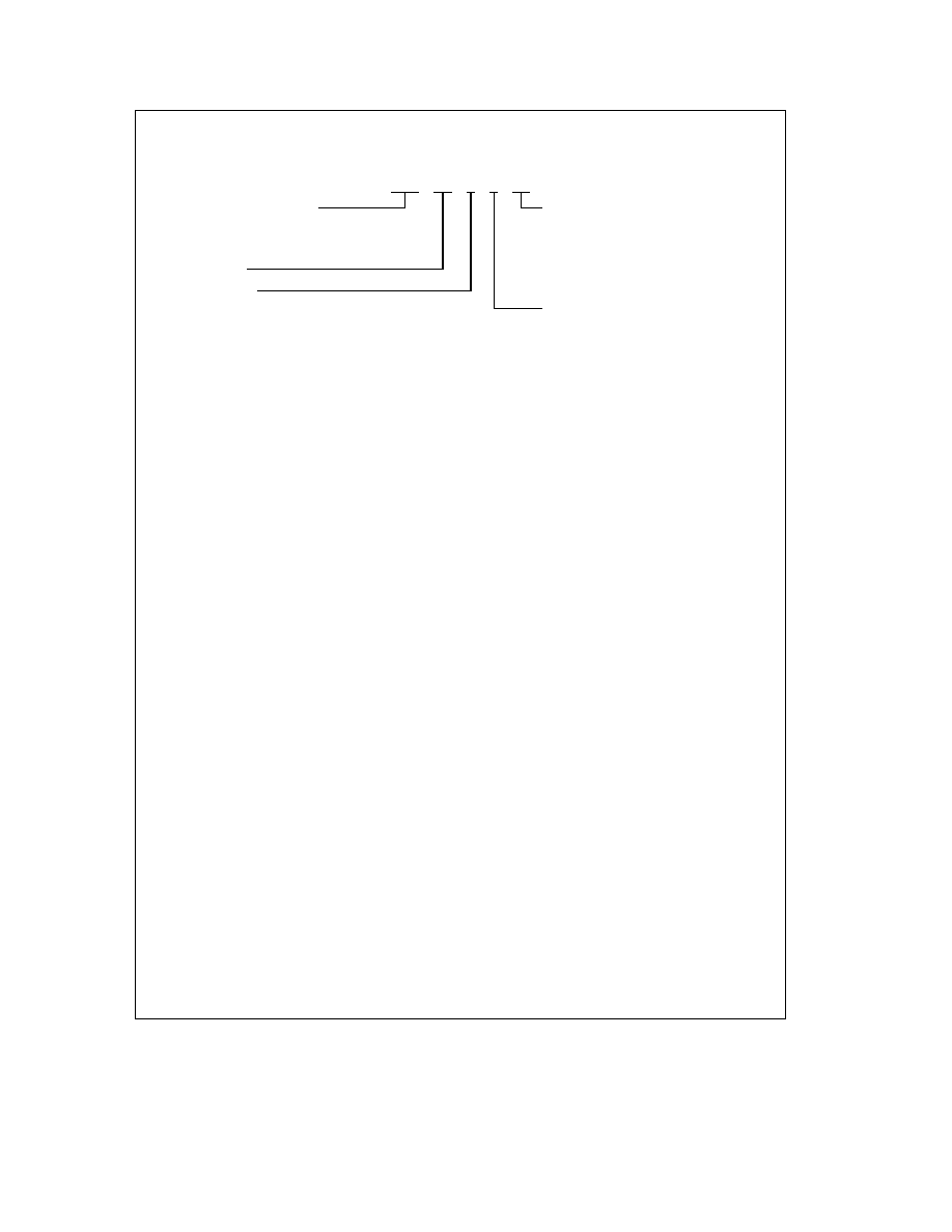
Logic Symbol
IEEE IEC
TL F 10692 ≠ 1
Connection Diagrams
Pin Assignment
for DIP SOIC and Flatpak
TL F 10692 ≠ 2
Pin Assignment
for LCC
TL F 10692 ≠ 3
Pin Names
Description
A
n
B
n
Inputs
O
n
Outputs
Function Table
Inputs
Output
A
n
B
n
O
n
L
L
L
L
H
H
H
X
Z
H
e
HIGH Voltage Level
L
e
LOW Voltage Level
Z
e
HIGH Impedance
X
e
Immaterial
TRI-STATE
is a registered trademark of National Semiconductor Corporation
FACT
TM
is a trademark of National Semiconductor Corporation
C1995 National Semiconductor Corporation
RRD-B30M75 Printed in U S A

Absolute Maximum Ratings
(Note 1)
If Military Aerospace specified devices are required
please contact the National Semiconductor Sales
Office Distributors for availability and specifications
Supply Voltage (V
CC
)
b
0 5V to
a
7 0V
DC Input Diode Current (I
K
)
V
I
e b
0 5V
b
20 mA
V
I
e
V
CC
a
0 5V
a
20 mA
DC Input Voltage (V
I
)
b
0 5V to V
CC
a
0 5V
DC Output Diode Current (I
OK
)
V
O
e b
0 5V
b
20 mA
V
O
e
V
CC
a
0 5V
a
20 mA
DC Output Voltage (V
O
)
b
0 5V to V
CC
a
0 5V
DC Output Source
or Sink Current (I
O
)
g
50 mA
DC V
CC
or Ground Current
per Output Pin (I
CC
or I
GND
)
g
50 mA
Storage Temperature (T
STG
)
b
65 C to
a
150 C
Junction Temperature (T
J
)
CDIP
175 C
PDIP
140 C
Note 1
Absolute maximum ratings are those values beyond which damage
to the device may occur The databook specifications should be met without
exception to ensure that the system design is reliable over its power supply
temperature and output input loading variables National does not recom-
mend operation of FACT
TM
circuits outside databook specifications
Recommended Operating
Conditions
Supply Voltage (V
CC
)
'AC
2 0V to 6 0V
'ACT
4 5V to 5 5V
Input Voltage (V
I
)
0V to V
CC
Output Voltage (V
O
)
0V to V
CC
Operating Temperature (T
A
)
74AC ACT
b
40 C to
a
85 C
54AC ACT
b
55 C to
a
125 C
Minimum Input Edge Rate (DV Dt)
'AC Devices
V
IN
from 30% to 70% of V
CC
V
CC
3 3V 4 5V 5 5V
125 mV ns
Minimum Input Edge Rate (DV Dt)
'ACT Devices
V
IN
from 0 8V to 2 0V
V
CC
4 5V 5 5V
125 mV ns
DC Characteristics for 'AC Family Devices
74AC
54AC
74AC
Symbol
Parameter
V
CC
T
A
e a
25 C
T
A
e
T
A
e
Units
Conditions
(V)
b
55 C to
a
125 C
b
40 C to
a
85 C
Typ
Guaranteed Limits
V
IH
Minimum High Level
3 0
1 5
2 1
2 1
2 1
V
OUT
e
0 1V
Input Voltage
4 5
2 25
3 15
3 15
3 15
V
or V
CC
b
0 1V
5 5
2 75
3 85
3 85
3 85
V
IL
Maximum Low Level
3 0
1 5
0 9
0 9
0 9
V
OUT
e
0 1V
Input Voltage
4 5
2 25
1 35
1 35
1 35
V
or V
CC
b
0 1V
5 5
2 75
1 65
1 65
1 65
V
OH
Minimum High Level
3 0
2 99
2 9
2 9
2 9
I
OUT
e b
50 mA
Output Voltage
4 5
4 49
4 4
4 4
4 4
V
5 5
5 49
5 4
5 4
5 4
V
IN
e
V
IL
or V
IH
3 0
2 56
2 4
2 46
b
12 mA
4 5
3 86
3 7
3 76
V
I
OH
b
24 mA
5 5
4 86
4 7
4 76
b
24 mA
V
OL
Maximum Low Level
3 0
0 002
0 1
0 1
0 1
I
OUT
e
50 mA
Output Voltage
4 5
0 001
0 1
0 1
0 1
V
5 5
0 001
0 1
0 1
0 1
V
IN
e
V
IL
or V
IH
3 0
0 36
0 50
0 44
12 mA
4 5
0 36
0 50
0 44
V
I
OL
24 mA
5 5
0 36
0 50
0 44
24 mA
I
IN
Maximum Input
5 5
g
0 1
g
1 0
g
1 0
m
A
V
I
e
V
CC
GND
Leakage Current
All outputs loaded thresholds on input associated with output under test
2

DC Characteristics for 'AC Family Devices
(Continued)
74AC
54AC
74AC
Symbol
Parameter
V
CC
T
A
e a
25 C
T
A
e
T
A
e
Units
Conditions
(V)
b
55 C to
a
125 C
b
40 C to
a
85 C
Typ
Guaranteed Limits
I
OZ
Maximum TRI-STATE
V
I
(OE)
e
V
IL
V
IH
Current
5 5
g
0 5
g
10 0
g
5 0
m
A
V
I
e
V
CC
V
GND
V
O
e
V
CC
GND
I
OLD
Minimum Dynamic
5 5
50
75
mA
V
OLD
e
1 65V Max
I
OHD
Output Current
5 5
b
50
b
75
mA
V
OHD
e
3 85V Min
I
CC
Maximum Quiescent
5 5
4 0
80 0
40 0
m
A
V
IN
e
V
CC
Supply Current
or GND
Maximum test duration 2 0 ms one output loaded at a time
Note
I
IN
and I
CC
3 0V are guaranteed to be less than or equal to the respective limit
5 5V V
CC
I
CC
for 54AC
25 C is identical to 74AC
25 C
DC Characteristics for 'ACT Family Devices
74ACT
74ACT
Symbol
Parameter
V
CC
T
A
e a
25 C
T
A
e
Units
Conditions
(V)
b
40 C to
a
85 C
Typ
Guaranteed Limits
V
IH
Minimum High Level
4 5
1 5
2 0
2 0
V
V
OUT
e
0 1V
Input Voltage
5 5
1 5
2 0
2 0
or V
CC
b
0 1V
V
IL
Maximum Low Level
4 5
1 5
0 8
0 8
V
V
OUT
e
0 1V
Input Voltage
5 5
1 5
0 8
0 8
or V
CC
b
0 1V
V
OH
Minimum High Level
4 5
4 49
4 4
4 4
V
I
OUT
e b
50 mA
Output Voltage
5 5
5 49
5 4
5 4
V
IN
e
V
IL
or V
IH
4 5
3 86
3 76
V
I
OH
b
24 mA
5 5
4 86
4 76
b
24 mA
V
OL
Maximum Low Level
4 5
0 001
0 1
0 1
V
I
OUT
e
50 mA
Output Voltage
5 5
0 001
0 1
0 1
V
IN
e
V
IL
or V
IH
4 5
0 36
0 44
V
I
OL
24 mA
5 5
0 36
0 44
24 mA
I
IN
Maximum Input Leakage Current
5 5
g
0 1
g
1 0
m
A
V
I
e
V
CC
GND
I
OZ
Maximum TRI-STATE
5 5
g
0 5
g
5 0
m
A
V
I
e
V
IL
V
IH
Current
V
O
e
V
CC
GND
I
CCT
Maximum I
CC
Input
5 5
0 6
1 5
mA
V
I
e
V
CC
b
2 1V
I
OLD
Minimum Dynamic
5 5
75
mA
V
OLD
e
1 65V Max
I
OHD
Output Current
5 5
b
75
mA
V
OHD
e
3 85V Min
I
CC
Maximum Quiescent
5 5
4 0
40 0
m
A
V
IN
e
V
CC
Supply Current
or GND
All outputs loaded thresholds on input associated with output under test
Maximum test duration 2 0 ms one output loaded at a time
May be measured per the JEDEC Alternate Method
3

AC Electrical Characteristics
74AC
54AC
74AC
V
CC
T
A
e a
25 C
T
A
e b
55 C
T
A
e b
40 C
Symbol
Parameter
(V)
C
L
e
50 pF
to
a
125 C
to
a
85 C
Units
C
L
e
50 pF
C
L
e
50 pF
Min
Typ
Max
Min
Max
Min
Max
t
PLH
Propagation Delay
3 3
1 0
6 5
9 0
1 0
10 0
ns
Data to Output
5 0
1 0
5 5
7 0
1 0
7 5
t
PHL
Propagation Delay
3 3
1 0
6 5
9 0
1 0
10 0
ns
Data to Output
5 0
1 0
5 0
7 0
1 0
7 5
t
PZH
Output Enable Time
3 3
1 0
6 0
10 5
1 0
11 0
ns
5 0
1 0
5 0
7 0
1 0
8 0
t
PZL
Output Enable Time
3 3
1 0
7 5
10 0
1 0
11 0
ns
5 0
1 0
5 5
8 0
1 0
8 5
t
PHZ
Output Disable Time
3 3
1 0
7 5
10 0
1 0
10 5
ns
5 0
1 0
6 5
9 0
1 0
9 5
t
PLZ
Output Disable Time
3 3
1 0
7 5
10 5
1 0
11 5
ns
5 0
1 0
6 5
9 0
1 0
9 5
Voltage Range 3 3 is 3 3V
g
0 3V
Voltage Range 5 0 is 5 0V
g
0 5V
AC Electrical Characteristics
74ACT
74ACT
V
CC
T
A
e a
25 C
T
A
e b
40 C
Symbol
Parameter
(V)
C
L
e
50 pF
to
a
85 C
Units
C
L
e
50 pF
Min
Typ
Max
Min
Max
t
PLH
Propagation Delay
5 0
1 0
6 5
9 0
1 0
10 0
ns
Data to Output
t
PHL
Propagation Delay
5 0
1 0
7 0
9 0
1 0
10 0
ns
Data to Output
t
PZH
Output Enable Time
5 0
1 0
6 0
8 5
1 0
9 5
ns
t
PZL
Output Enable Time
5 0
1 0
7 0
9 5
1 0
10 5
ns
t
PHZ
Output Disable Time
5 0
1 0
7 0
9 5
1 0
10 5
ns
t
PLZ
Output Disable Time
5 0
1 0
7 5
10 0
1 0
10 5
ns
Voltage Range 5 0 is 5 0V
g
0 5V
Capacitance
Symbol
Parameter
AC ACT
Units
Conditions
Typ
C
IN
Input Capacitance
4 5
pF
V
CC
e
OPEN
C
PD
Power Dissipation
45 0
pF
V
CC
e
5 0V
Capacitance
4
Ordering Information
The device number is used to form part of a simplified purchasing code where the package type and temperature range are
defined as follows
74AC
125
P
C
QR
Temperature Range Family
Special Variations
74AC
e
Commercial
X
e
Devices shipped in 13 reels
54AC
e
Military
QR
e
Commercial grade device
74ACT
e
Commercial TTL-Compatible
with burn-in
QB
e
Military grade device with
Device Type
environmental and burn-in
processing shipped in tubes
Package Code
P
e
Plastic DIP
Temperature Range
D
e
Ceramic DIP
C
e
Commercial (
b
40 C to
a
85 C)
F
e
Flatpak
M
e
Military (
b
55 C to
a
125 C)
L
e
Leadless Ceramic Chip Carrier (LCC)
S
e
Small Outline (SOIC)
5