 | –≠–ª–µ–∫—Ç—Ä–æ–Ω–Ω—ã–π –∫–æ–º–ø–æ–Ω–µ–Ω—Ç: 54AC540F | –°–∫–∞—á–∞—Ç—å:  PDF PDF  ZIP ZIP |

54AC540
Octal Buffer/Line Driver with TRI-STATE
Æ
Outputs
General Description
The 'AC540 is an octal buffer/line drivers designed to be em-
ployed as memory and address drivers, clock drivers and
bus oriented transmitter/receivers.
These devices are similar in function to the 'AC240 while
providing flow-through architecture (inputs on opposite side
from outputs). This pinout arrangement makes these devices
especially useful as output ports for microprocessors, allow-
ing ease of layout and greater PC board density.
Features
n
I
CC
and I
OZ
reduced by 50%
n
TRI-STATE inverting outputs
n
Inputs and outputs opposite side of package, allowing
easier interface to microprocessors
n
Output source/sink 24 mA
n
Standard Military Drawing 54AC540: 5962-8769501
Logic Symbol
Truth Table
Inputs
Outputs
OE
1
OE
2
I
L
L
H
L
H
X
X
Z
X
H
X
Z
L
L
L
H
H = HIGH Voltage Level
L = LOW Voltage Level
X = Immaterial
Z = High Impedance
TRI-STATE
Æ
is a registered trademark of National Semiconductor Corporation.
FACT
TM
is a trademark of Fairchild Semiconductor Corporation.
IEEE/IEC
DS100293-1
July 1998
54AC540
Octal
Buffer/Line
Driver
with
TRI-ST
A
T
E
Outputs
© 1998 National Semiconductor Corporation
DS100293
www.national.com
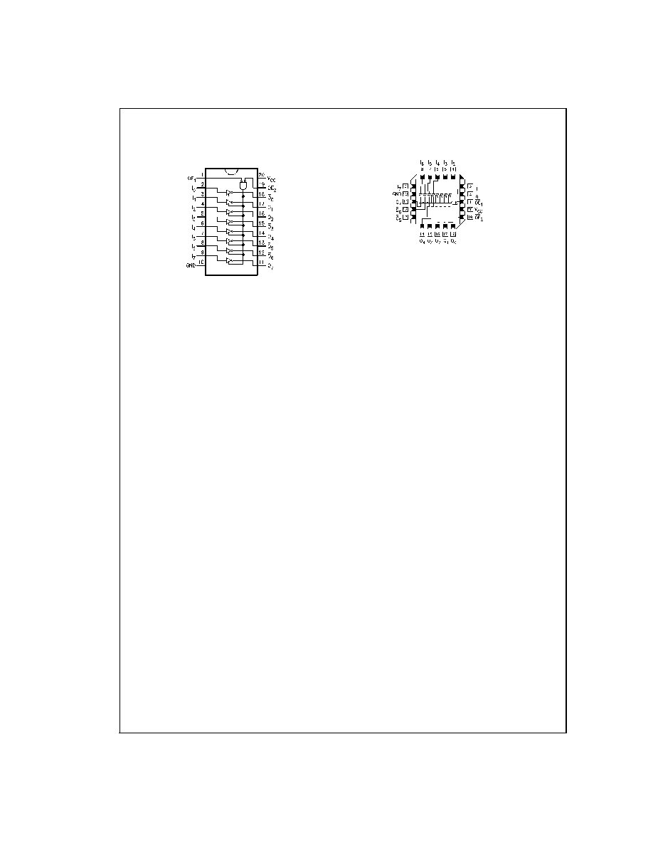
Connection Diagrams
Pin Assignment
for DIP and Flatpak
DS100293-3
Pin Assignment for LCC
DS100293-2
www.national.com
2

Absolute Maximum Ratings
(Note 1)
If Military/Aerospace specified devices are required,
please contact the National Semiconductor Sales Office/
Distributors for availability and specifications.
Supply Voltage (V
CC
)
-0.5V to +7.0V
DC Input Diode Current (I
IK
)
V
I
= -0.5V
-20 mA
V
I
= V
CC
+ 0.5V
+20 mA
DC Input Voltage (V
I
)
-0.5V to V
CC
+ 0.5V
DC Output Diode Current (I
OK
)
V
O
= -0.5V
-20 mA
V
O
= V
CC
+ 0.5V
+20 mA
DC Output Voltage (V
O
)
-0.5V to V
CC
+ 0.5V
DC Output Source
or Sink Current (I
O
)
±
50 mA
DC V
CC
or Ground Current
per Output Pin (I
CC
or I
GND
)
±
50 mA
Storage Temperature (T
STG
)
-65∞C to +150∞C
Junction Temperature (T
J
)
CDIP
175∞C
Recommended Operating
Conditions
Supply Voltage (V
CC
)
'AC
2.0V to 6.0V
Input Voltage (V
I
)
0V to V
CC
Output Voltage (V
O
)
0V to V
CC
Operating Temperature (T
A
)
54AC
-55∞C to +125∞C
Minimum Input Edge Rate (
V/
t)
'AC Devices
V
IN
from 30% to 70% of V
CC
V
CC
@
3.3V, 4.5V, 5.5V
125 mV/ns
Note 1: Absolute maximum ratings are those values beyond which damage
to the device may occur. The databook specifications should be met, without
exception, to ensure that the system design is reliable over its power supply,
temperature, and output/input loading variables. National does not recom-
mend operation of FACT
TM
circuits outside databook specifications.
DC Characteristics for 'AC Family Devices
54AC
Symbol
Parameter
V
CC
T
A
=
Units
Conditions
(V)
-55∞C to +125∞C
Guaranteed Limits
V
IH
Minimum High Level
3.0
2.1
V
OUT
= 0.1V
Input Voltage
4.5
3.15
V
or V
CC
- 0.1V
5.5
3.85
V
IL
Maximum Low Level
3.0
0.9
V
OUT
= 0.1V
Input Voltage
4.5
1.35
V
or V
CC
- 0.1V
5.5
1.65
V
OH
Minimum High Level
3.0
2.9
I
OUT
= -50 µA
Output Voltage
4.5
4.4
V
5.5
5.4
(Note 2)
V
IN
= V
IL
or V
IH
3.0
2.4
I
OH
= -12 mA
4.5
3.7
V
I
OH
= -24 mA
5.5
4.7
I
OH
= -24 mA
V
OL
Maximum Low Level
3.0
0.1
I
OUT
= 50 µA
Output Voltage
4.5
0.1
V
5.5
0.1
(Note 2)
V
IN
= V
IL
or V
IH
3.0
0.50
I
OL
= 12 mA
4.5
0.50
V
I
OL
= 24 mA
5.5
0.50
I
OL
= 24 mA
I
IN
Maximum Input
5.5
±
1.0
µA
V
I
= V
CC
, GND
Leakage Current
I
OZ
Maximum TRI-STATE
V
I
(OE) = V
IL
, V
IH
Current
5.5
±
5.0
µA
V
I
= V
CC
, GND
V
O
= V
CC
, GND
3
www.national.com
DC Characteristics for 'AC Family Devices
(Continued)
54AC
Symbol
Parameter
V
CC
T
A
=
Units
Conditions
(V)
-55∞C to +125∞C
Guaranteed Limits
(Note 3)
I
OLD
Minimum Dynamic
5.5
50
mA
V
OLD
= 1.65V Max
I
OHD
Output Current
5.5
-50
mA
V
OHD
= 3.85V Min
I
CC
Maximum Quiescent
5.5
80.0
µA
V
IN
= V
CC
Supply Current
or GND
Note 2: All outputs loaded; thresholds on input associated with output under test.
Note 3: Maximum test duration 2.0 ms, one output loaded at a time.
Note 4: I
IN
and I
CC
@
3.0V are guaranteed to be less than or equal to the respective limit
@
5.5V V
CC
.
I
CC
for 54AC
@
25∞C is identical to 74AC
@
25∞C.
AC Electrical Characteristics
54AC
V
CC
T
A
= -55∞C
Symbol
Parameter
(V)
to +125∞C
Units
(Note 5)
C
L
= 50 pF
Min
Max
t
PLH
Propagation Delay
3.3
1.0
9.0
ns
Data to Output
5.0
1.5
7.0
t
PHL
Propagation Delay
3.3
1.0
8.0
ns
Data to Output
5.0
1.5
6.5
t
PZH
Output Enable Time
3.3
1.0
13.0
ns
5.0
1.5
10.0
t
PZL
Output Enable Time
3.3
1.0
12.0
ns
5.0
1.5
9.0
t
PHZ
Output Disable Time
3.3
1.0
15.5
ns
5.0
1.5
12.0
t
PLZ
Output Disable Time
3.3
1.0
12.0
ns
5.0
1.5
10.0
Note 5: Voltage Range 3.3 is 3.3V
±
0.3V
Voltage Range 5.0 is 5.0V
±
0.5V
Capacitance
Symbol
Parameter
Typ
Units
Conditions
C
IN
Input Capacitance
4.5
pF
V
CC
= OPEN
C
PD
Power Dissipation
30.0
pF
V
CC
= 5.0V
Capacitance
www.national.com
4
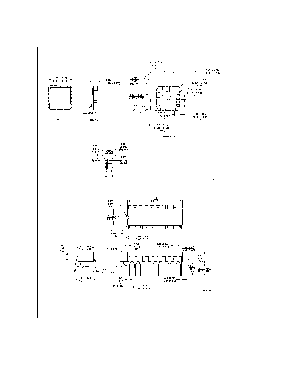
Physical Dimensions
inches (millimeters) unless otherwise noted
20-Terminal Ceramic Leadless Chip Carrier (L)
NS Package Number E20A
20-Lead Ceramic Dual-In-Line Package (D)
NS Package Number J20A
5
www.national.com