 | –≠–ª–µ–∫—Ç—Ä–æ–Ω–Ω—ã–π –∫–æ–º–ø–æ–Ω–µ–Ω—Ç: 54ACT258 | –°–∫–∞—á–∞—Ç—å:  PDF PDF  ZIP ZIP |
54AC258
∑
54ACT258
Quad 2-Input Multiplexer with TRI-STATE
Æ
Outputs
General Description
The 'AC/'ACT258 is a quad 2-input multiplexer with
TRI-STATE outputs. Four bits of data from two sources can
be selected using a common data select input. The four out-
puts present the selected data in the complement (inverted)
form. The outputs may be switched to a high impedance
state with a HIGH on the common Output Enable (OE) input,
allowing the outputs to interface directly with bus-oriented
systems.
Features
n
I
CC
and I
OZ
reduced by 50%
n
Multiplexer expansion by tying outputs together
n
Inverting TRI-STATE outputs
n
Outputs source/sink 24 mA
n
'ACT258 has TTL-compatible inputs
n
Standard Military Drawing (SMD)
-- 'ACT258: 5962-88704
-- 'AC258: 5962-91604
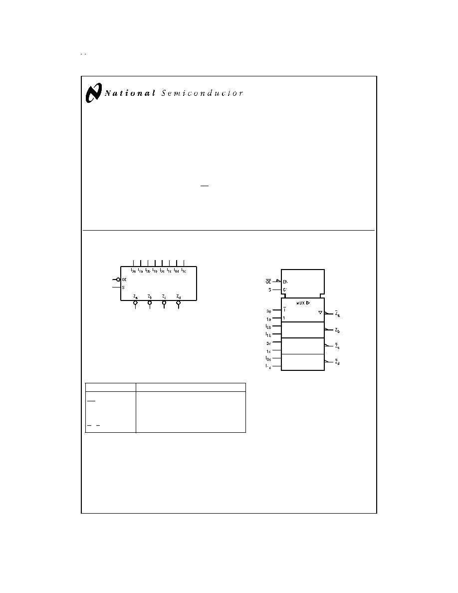
Logic Symbols
Pin Names
Description
S
Common Data Select Input
OE
TRI-STATE Output Enable Input
I
0a
≠I
0d
Data Inputs from Source 0
I
1a
≠I
1d
Data Inputs from Source 1
Z
a
≠Z
d
TRI-STATE Inverting Data Outputs
TRI-STATE
Æ
is a registered trademark of National Semiconductor Corporation.
FACT
Æ
is a registered trademark of Fairchild Semiconductor Corporation.
DS100287-1
IEEE/IEC
DS100287-2
August 1998
54AC258
∑
54ACT258
Quad
2-Input
Multiplexer
with
TRI-ST
A
T
E
Outputs
© 1998 National Semiconductor Corporation
DS100287
www.national.com
Connection Diagrams
Functional Description
The 'AC/'ACT258 is a quad 2-input multiplexer with
TRI-STATE outputs. It selects four bits of data from two
sources under control of a common Select input (S). When
the Select input is LOW, the I
0x
inputs are selected and when
Select is HIGH, the I
1x
inputs are selected. The data on the
selected inputs appears at the outputs in inverted form. The
'AC/'ACT258 is the logic implementation of a 4-pole,
2-position switch where the position of the switch is deter-
mined by the logic levels supplied to the Select input. The
logic equations for the outputs are shown below:
Z
a
= OE ∑ (I
1a
∑ S + I
0a
∑ S)
Z
b
= OE ∑ (I
1b
∑ S + I
0b
∑ S)
Z
c
= OE ∑ (I
1c
∑ S + I
0c
∑ S)
Z
d
= OE ∑ (I
1d
∑ S + I
0d
∑ S)
When the Output Enable input (OE) is HIGH, the outputs are
forced to a high impedance state. If the outputs of the
TRI-STATE devices are tied together, all but one device must
be in the high impedance state to avoid high currents that
would exceed the maximum ratings. Designers should en-
sure that Output Enable signals to TRI-STATE devices
whose outputs are tied together are designed so there is no
overlap.
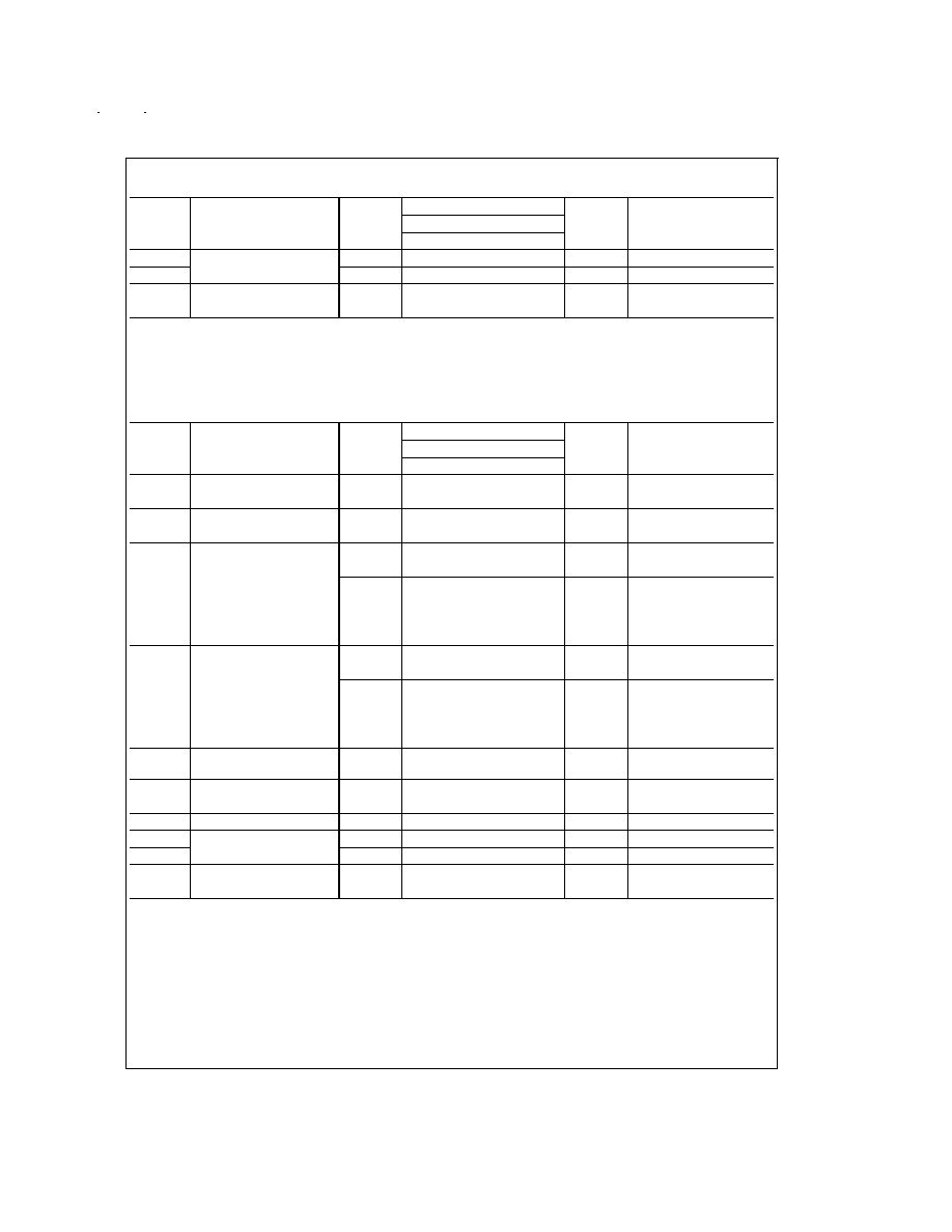
Truth Table
Output
Select
Data
Outputs
Enable
Input
Inputs
OE
S
I
0
I
1
Z
H
X
X
X
Z
L
H
X
L
H
L
H
X
H
L
L
L
L
X
H
L
L
H
X
L
H = HIGH Voltage Level
L = LOW Voltage Level
X = Immaterial
Z = High Impedance
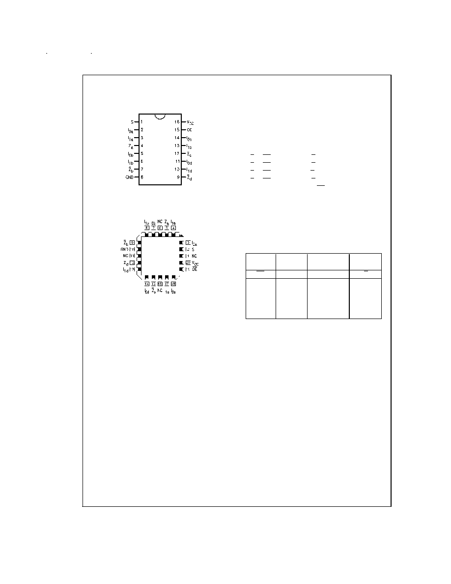
Pin Assignment
for DIP and Flatpak
DS100287-3
Pin Assignment
for LCC
DS100287-4
www.national.com
2
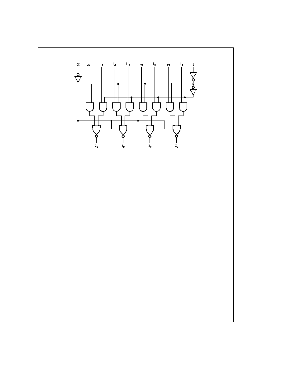
Logic Diagram
DS100287-5
Please note that this diagram is provided only for the understanding of logic operations and should not be used to estimate propagation delays.
www.national.com
3
Absolute Maximum Ratings
(Note 1)
If Military/Aerospace specified devices are required,
please contact the National Semiconductor Sales Office/
Distributors for availability and specifications.
Supply Voltage (V
CC
)
-0.5V to +7.0V
DC Input Diode Current (I
IK
)
V
I
= -0.5V
-20 mA
V
I
= V
CC
+ 0.5V
+20 mA
DC Input Voltage (V
I
)
-0.5V to V
CC
+ 0.5V
DC Output Diode Current (I
OK
)
V
O
= -0.5V
-20 mA
V
O
= V
CC
+ 0.5V
+20 mA
DC Output Voltage (V
O
)
-0.5V to V
CC
+ 0.5V
DC Output Source
or Sink Current (I
O
)
±
50 mA
DC V
CC
or Ground Current
per Output Pin (I
CC
or I
GND
)
±
50 mA
Storage Temperature (T
STG
)
-65∞C to +150∞C
Junction Temperature (T
J
)
CDIP
175∞C
Recommended Operating
Conditions
Supply Voltage (V
CC
)
'AC
2.0V to 6.0V
'ACT
4.5V to 5.5V
Input Voltage (V
I
)
0V to V
CC
Output Voltage (V
O
)
0V to V
CC
Operating Temperature (T
A
)
54AC/ACT
-55∞C to +125∞C
Minimum Input Edge Rate (
V/
t)
'AC Devices
V
IN
from 30% to 70% of V
CC
V
CC
@
3.3V 4.5V, 5.5V
125 mV/ns
Minimum Input Edge Rate (
V/
t)
'ACT Devices
V
IN
from 0.8V to 2.0V
V
CC
@
4.5V, 5.5V
125 mV/ns
Note 1: Absolute maximum ratings are those values beyond which damage
to the device may occur. The databook specifications should be met, without
exception, to ensure that the system design is reliable over its power supply,
temperature, and output/input loading variables. National does not recom-
mend operation of FACT
Æ
circuits outside databook specifications.
DC Characteristics for 'AC Family Devices
54AC
Symbol
Parameter
V
CC
T
A
= -55∞C to +125∞C
Units
Conditions
(V)
Guaranteed Limits
V
IH
Minimum High Level
3.0
2.1
V
OUT
= 0.1V
Input Voltage
4.5
3.15
V
or V
CC
- 0.1V
5.5
3.85
V
IL
Maximum Low Level
3.0
0.9
V
OUT
= 0.1V
Input Voltage
4.5
1.35
V
or V
CC
- 0.1V
5.5
1.65
V
OH
Minimum High Level
3.0
2.9
I
OUT
= -50 µA
Output Voltage
4.5
4.4
V
5.5
5.4
(Note 2)
V
IN
= V
IL
or V
IH
3.0
2.4
I
OH
= -12 mA
4.5
3.7
V
I
OH
= -24 mA
5.5
4.7
I
OH
= -24 mA
V
OL
Maximum Low Level
3.0
0.1
I
OUT
= 50 µA
Output Voltage
4.5
0.1
V
5.5
0.1
(Note 2)
V
IN
= V
IL
or V
IH
3.0
0.50
I
OL
= 12 mA
4.5
0.50
V
I
OL
= 24 mA
5.5
0.50
I
OL
= 24 mA
I
IN
Maximum Input
5.5
±
1.0
µA
V
I
= V
CC
, GND
Leakage Current
I
OZ
Maximum TRI-STATE
V
I
(OE) = V
IL
, V
IH
Current
5.5
±
5.0
µA
V
I
= V
CC
, GND
V
O
= V
CC
, GND
www.national.com
4
DC Characteristics for 'AC Family Devices
(Continued)
54AC
Symbol
Parameter
V
CC
T
A
= -55∞C to +125∞C
Units
Conditions
(V)
Guaranteed Limits
I
OLD
Minimum Dynamic
5.5
50
mA
V
OLD
= 1.65V Max
I
OHD
Output Current (Note 3)
5.5
-50
mA
V
OHD
= 3.85V Min
I
CC
Maximum Quiescent
5.5
80.0
µA
V
IN
= V
CC
Supply Current
or GND
Note 2: All outputs loaded; thresholds on input associated with output under test.
Note 3: Maximum test duration 2.0 ms, one output loaded at a time.
Note 4: I
IN
and I
CC
@
3.0V are guaranteed to be less than or equal to the respective limit
@
5.5V V
CC
.
I
CC
for 54AC
@
25∞C is identical to 74AC
@
25∞C.
DC Characteristics for 'ACT Family Devices
54ACT
Symbol
Parameter
V
CC
T
A
= -55∞C to +125∞C
Units
Conditions
(V)
Guaranteed Limits
V
IH
Minimum High Level
4.5
2.0
V
V
OUT
= 0.1V
Input Voltage
5.5
2.0
or V
CC
- 0.1V
V
IL
Maximum Low Level
4.5
0.8
V
V
OUT
= 0.1V
Input Voltage
5.5
0.8
or V
CC
- 0.1V
V
OH
Minimum High Level
4.5
4.4
V
I
OUT
= -50 µA
Output Voltage
5.5
5.4
(Note 5)
V
IN
= V
IL
or V
IH
4.5
3.70
V
I
OH
= -24 mA
5.5
4.70
I
OH
= -24 mA
V
OL
Maximum Low Level
4.5
0.1
V
I
OUT
= 50 µA
Output Voltage
5.5
0.1
(Note 5)
V
IN
= V
IL
or V
IH
4.5
0.50
V
I
OL
= 24 mA
5.5
0.50
I
OL
= 24 mA
I
IN
Maximum Input Leakage
Current
5.5
±
1.0
µA
V
I
= V
CC
, GND
I
OZ
Maximum TRI-STATE
5.5
±
5.0
µA
V
I
= V
IL
, V
IH
Current
V
O
= V
CC
, GND
I
CCT
Maximum I
CC
/Input
5.5
1.6
mA
V
I
= V
CC
- 2.1V
I
OLD
Minimum Dynamic
5.5
50
mA
V
OLD
= 1.65V Max
I
OHD
Output Current (Note 6)
5.5
-50
mA
V
OHD
= 3.85V Min
I
CC
Maximum Quiescent
5.5
80.0
µA
V
IN
= V
CC
Supply Current
or GND
Note 5: All outputs loaded; thresholds on input associated with output under test.
Note 6: Maximum test duration 2.0 ms, one output loaded at a time.
Note 7: I
CC
for 54ACT
@
25∞C is identical to 74ACT
@
25∞C.
www.national.com
5