
54AC299
∑
54ACT299
8-Input Universal Shift/Storage Register with Common
Parallel I/O Pins
General Description
The 'AC/'ACT299 is an 8-bit universal shift/storage register
with TRI-STATE
Æ
outputs. Four modes of operation are pos-
sible: hold (store), shift left, shift right and load data. The par-
allel load inputs and flip-flop outputs are multiplexed to re-
duce the total number of package pins. Additional outputs
are provided for flip-flops Q
0
, Q
7
to allow easy serial cascad-
ing. A separate active LOW Master Reset is used to reset the
register.
Features
n
I
CC
and I
OZ
reduced by 50%
n
Common parallel I/O for reduced pin count
n
Additional serial inputs and outputs for expansion
n
Four operating modes: shift left, shift right, load and
store
n
TRI-STATE outputs for bus-oriented applications
n
Outputs source/sink 24 mA
n
'ACT299 has TTL-compatible inputs
n
Standard Microcircuit Drawing (SMD)
'AC299: 5962-88754
'ACT299: 5962-88771
Ordering Code:
Logic Symbols
Connection Diagrams
TRI-STATE
Æ
is a registered trademark of National Semiconductor Corporation.
FACT
Æ
is a registered trademark of Fairchild Semiconductor Corporation.
DS100252-1
IEEE/IEC
DS100252-4
Pin Assignment
for DIP and Flatpak
DS100252-2
Pin Assignment for LCC
DS100252-3
September 1998
54ACC299
∑
54ACT299
8-Input
Universal
Shift/Storage
Register
with
Common
Parallel
I/O
Pins
© 1998 National Semiconductor Corporation
DS100252
www.national.com

Connection Diagrams
(Continued)
Pin Names
Description
CP
Clock Pulse Input
DS
0
Serial Data Input for Right Shift
DS
7
Serial Data Input for Left Shift
S
0
, S
1
Mode Select Inputs
MR
Asynchronous Master Reset
OE
1
, OE
2
TRI-STATE Output Enable Inputs
I/O
0
≠I/O
7
Parallel Data Inputs or
TRI-STATE Parallel Outputs
Q
0
, Q
7
Serial Outputs
Functional Description
The 'AC/'ACT299 contains eight edge-triggered D-type
flip-flops and the interstage logic necessary to perform syn-
chronous shift left, shift right, parallel load and hold opera-
tions. The type of operation is determined by S
0
and S
1
, as
shown in the Truth Table. All flip-flop outputs are brought out
through TRI-STATE buffers to separate I/O pins that also
serve as data inputs in the parallel load mode. Q
0
and Q
7
are
also brought out on other pins for expansion in serial shifting
of longer words.
A LOW signal on MR overrides the Select and CP inputs and
resets the flip-flops. All other state changes are initiated by
the rising edge of the clock. Inputs can change when the
clock is in either state provided only that the recommended
setup and hold times, relative to the rising edge of CP, are
observed.
A HIGH signal on either OE
1
or OE
2
disables the TRI-STATE
buffers and puts the I/O pins in the high impedance state. In
this condition the shift, hold, load and reset operations can
still occur. The TRI-STATE buffers are also disabled by HIGH
signals on both S
0
and S
1
in preparation for a parallel load
operation.
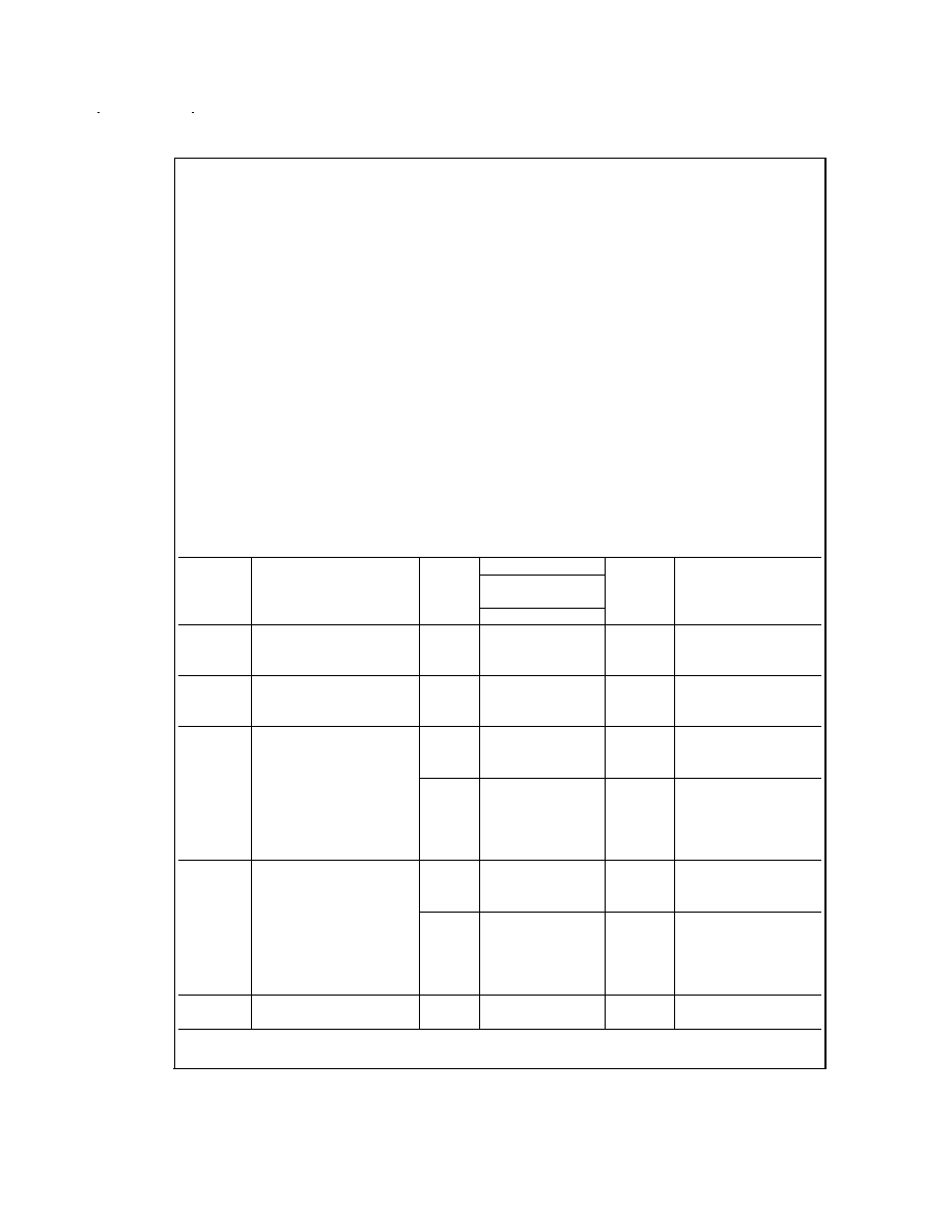
Truth Table
Inputs
Response
MR
S
1
S
0
CP
L
X
X
X
Asynchronous Reset;
Q
0
≠Q
7
= LOW
H
H
H
N
Parallel Load; I/O
n
Q
n
H
L
H
N
Shift Right; DS
0
Q
0
,
Q
0
Q
1
, etc.
H
H
L
N
Shift Left, DS
7
Q
7
,
Q
7
Q
6
, etc.
H
L
L
X
Hold
H = HIGH Voltage Level
L = LOW Voltage Level
X = Immaterial
N
= LOW-to-HIGH Transition
www.national.com
2

Logic Diagram
DS100252-5
Please note that this diagram is provided only for the understanding of logic operations and should not be used to estimate propagation delays.
www.national.com
3
Absolute Maximum Ratings
(Note 1)
If Military/Aerospace specified devices are required,
please contact the National Semiconductor Sales Office/
Distributors for availability and specifications.
Supply Voltage (V
CC
)
-0.5V to +7.0V
DC Input Diode Current (I
IK
)
V
I
= -0.5V
-20 mA
V
I
= V
CC
+0.5V
+20 mA
DC Input Voltage (V
I
)
-0.5V to V
CC
+0.5V
DC Output Diode Current (I
OK
)
V
O
= -0.5V
-20 mA
V
O
= V
CC
+0.5V
+20 mA
DC Output Voltage (V
O
)
-0.5V to V
CC
+0.5V
DC Output Source or Sink Current
(I
O
)
±
50 mA
DC V
CC
or Ground Current
Per Output Pin (I
CC
or I
GND
)
±
50 mA
Storage Temperature (T
STG
)
-65∞C to +150∞C
Junction Temperature (T
J
)
CDIP
175∞C
Recommended Operating
Conditions
Supply Voltage (V
CC
)
(Unless Otherwise Specified)
'AC
2.0V to 6.0V
'ACT
4.5V to 5.0V
Input Voltage (V
I
)
0V to V
CC
Output Voltage (V
O
)
0V to V
CC
Operating Temperature (T
A
)
54AC/ACT
-55∞C to +125∞C
Minimum Input Edge Rate (
V/
t)
'AC Devices
V
IN
from 30% to 70% of V
CC
V
CC
@
3.3V, 4.5V, 5.5V
125 mV/ns
Minimum Input Edge Rate (
V/
t)
'ACT Devices
V
IN
from 0.8V to 2.0V
V
CC
@
4.5V, 5.5V
125 mV/ns
Note 1: Absolute maximum ratings are those values beyond which damage
to the device may occur. Obviously the databook specifications should be
met, without exception, to ensure that the system design is reliable over its
power supply, temperature, and output/input loading variables. National does
not recommend operation of FACT
Æ
circuits outside databook specifications.
DC Electrical Characteristics
For 'AC Family Devices
54AC
Symbol
Parameter
V
CC
T
A
=
Units
Conditions
(V)
-55∞C to +125∞C
Guaranteed Limits
V
IH
Minimum High Level
3.0
2.1
V
OUT
= 0.1V
Input Voltage
4.5
3.15
V
or V
CC
- 0.1V
5.5
3.85
V
IL
Maximum Low Level
3.0
0.9
V
OUT
= 0.1V
Input Voltage
4.5
1.35
V
or V
CC
- 0.1V
5.5
1.65
V
OH
Minimum High Level
3.0
2.9
I
OUT
= -50 µA
Output Voltage
4.5
4.4
V
5.5
5.4
(Note 2)
V
IN
= V
IL
or V
IH
3.0
2.4
V
I
OH
= -12 mA
4.5
3.7
I
OH
= -24 mA
5.5
4.7
I
OH
= -24 mA
V
OL
Maximum Low Level
3.0
0.1
I
OUT
= 50 µA
Output Voltage
4.5
0.1
V
5.5
0.1
(Note 2)
V
IN
= V
IL
or V
IH
3.0
0.50
I
OH
= 12 mA
4.5
0.50
V
I
OH
= 24 mA
5.5
0.50
I
OH
= 24 mA
I
IN
Maximum Input
5.5
±
1.0
µA
V
I
= V
CC
, GND
Leakage Current
Note 2: All outputs loaded; threshold on input associated with output under test.
www.national.com
4

DC Electrical Characteristics
For 'AC Family Devices
54AC
Symbol
Parameter
V
CC
T
A
=
Units
Conditions
(V)
-55∞C to +125∞C
Guaranteed Limits
(Note 4)
I
OLD
Minimum Dynamic
5.5
50
mA
V
OLD
= 1.65V Max
I
OHD
Output Current
5.5
-50
mA
V
OHD
= 3.85V Min
I
CC
Maximum Quiescent
5.5
80.0
µA
V
IN
= V
CC
Supply Current
or GND
I
OZT
Maximum I/O
V
I
(OE) = V
IL
, V
IH
Leakage Current
5.5
±
5.5
µA
V
I
= V
CC
, GND
V
O
= V
CC
, GND
Note 3: All outputs loaded; threshold on input associated with output under test.
Note 4: Maximum test duration 20 ms, one output loaded at a time.
Note 5: I
IN
and I
CC
@
3.0V are guaranteed to be less than or equal to the respective limit
@
5.5V V
CC
.
I
CC
for 54AC
@
25∞C is identical to 74AC
@
25∞C.
DC Electrical Characteristics
For 'ACT Family Devices
54ACT
Symbol
Parameter
V
CC
T
A
=
Units
Conditions
(V)
-55∞C to +125∞C
Guaranteed Limits
V
IH
Minimum High Level
4.5
2.0
V
V
OUT
= 0.1V
Input Voltage
5.5
2.0
or V
CC
- 0.1V
V
IL
Maximum Low Level
3.0
0.8
V
OUT
= 0.1V
Input Voltage
4.5
0.8
or V
CC
- 0.1V
V
OH
Minimum High Level
4.5
4.4
V
I
OUT
= -50 µA
5.5
5.4
(Note 7)
V
IN
= V
IL
or V
IH
4.5
3.70
V
I
OH
= -24 mA
5.5
4.70
I
OH
= -24 mA
V
OL
Maximum Low Level
4.5
0.1
V
I
OUT
= 50 µA
Output Voltage
5.5
0.1
(Note 7)
V
IN
= V
IL
or V
IH
4.5
0.50
V
I
OL
= 24 mA
5.5
0.50
I
OL
= 24 mA
I
IN
Maximum Input
5.5
±
1.0
µA
V
I
= V
CC
, GND
Leakage Current
I
CCT
Maximum I
CC
/Input
5.5
1.6
mA
V
I
= V
CC
- 2.1V
(Note 8)
I
OLD
Minimum Dynamic
5.5
50
mA
V
OLD
= 1.65V Max
I
OHD
Output Current
5.5
-50
mA
V
OHD
= 3.85V Min
I
CC
Maximum Quiescent
5.5
80.0
µA
V
IN
= V
CC
Supply Current
or GND
I
OZT
Maximum I/O
V
I
(OE) = V
IL
, V
IH
Leakage Current
5.5
±
5.0
µA
V
I
= V
CC
, GND
V
O
= V
CC
, GND
www.national.com
5