54ACTQ533
Quiet Series Octal Transparent Latch with TRI-STATE
Æ
Outputs
General Description
The ACTQ533 consists of eight latches with TRI-STATE out-
puts for bus organized system applications. The flip-flops ap-
pear transparent to the data when Latch Enable (LE) is
HIGH. When LE is low, the data satisfying the input timing re-
quirements is latched. Data appears on the bus when the
Output Enable (OE) is LOW. When OE is HIGH, the bus out-
put is in the high impedance state.
The ACTQ533 utilizes NSC Quiet Series technology to guar-
antee quiet output switching and improve dynamic threshold
performance. FACT Quiet Series
TM
features GTO
TM
output
control and undershoot corrector in addition to a split ground
bus for superior performance.
Features
n
I
CC
and I
OZ
reduced by 50%
n
Guaranteed simultaneous switching noise level and
dynamic threshold performance
n
Improved latch up immunity
n
Eight latches in a single package
n
TRI-STATE outputs drive bus lines or buffer memory
address registers
n
Outputs source/sink 24 mA
n
Inverted version of the ACTQ373
n
4 kV minimum ESD immunity
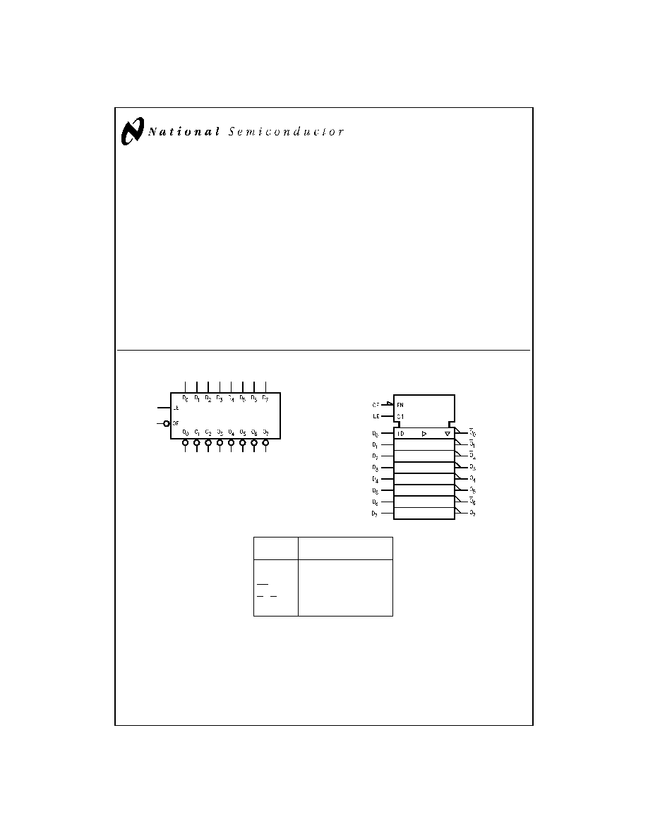
Logic Symbols
Pin
Names
Description
D
0
≠D
7
Data Inputs
LE
Latch Enable Input
OE
Output Enable Input
O
0
≠O
7
TRI-STATE Latch
Outputs
GTO
TM
is a trademark of National Semiconductor Corporation.
TRI-STATE
Æ
is a registered trademark of National Semiconductor Corporation.
FACT
Æ
is a registered trademark of Fairchild Semiconductor Corporation.
FACT Quiet Series
TM
is a trademark of Fairchild Semiconductor Corporation.
DS100241-1
IEEE/IEC
DS100241-2
August 1998
54ACTQ533
Quiet
Series
Octal
T
ransparent
Latch
with
TRI-ST
A
T
E
Outputs
© 1998 National Semiconductor Corporation
DS100241
www.national.com

Connection Diagrams
Functional Description
The ACTQ533 contains eight D-type latches with TRI-STATE
standard outputs. When the Latch Enable (LE) input is
HIGH, data on the D
n
inputs enters the latches. In this con-
dition the latches are transparent, i.e., a latch output will
change state each time its D input changes. When LE is
LOW, the latches store the information that was present on
the D inputs a setup time preceding the HIGH-to-LOW tran-
sition of LE. The TRI-STATE standard outputs are controlled
by the Output Enable (OE) input. When OE is LOW, the stan-
dard outputs are in the 2-state mode. When OE is HIGH, the
standard outputs are in the high impedance mode but this
does not interfere with entering new data into the latches.
Truth Table
Inputs
Outputs
LE
OE
D
n
O
n
X
H
X
Z
H
L
L
H
H
L
H
L
L
L
X
O
0
H = HIGH Voltage Level
L = LOW Voltage Level
Z = High Impedance
X = Immaterial
O
0
= Previous O
0
before HIGH to Low transition of Latch Enable
Logic Diagram
Pin Assignment
for DIP and Flatpak
DS100241-3
Pin Assignment
for LCC
DS100241-4
DS100241-5
Please note that this diagram is provided only for the understanding of logic operations and should not be used to estimate propagation delays.
www.national.com
2

Absolute Maximum Ratings
(Note 1)
If Military/Aerospace specified devices are required,
please contact the National Semiconductor Sales Office/
Distributors for availability and specifications.
Supply Voltage (V
CC
)
-0.5V to +7.0V
DC Input Diode Current (I
IK
)
V
I
= -0.5V
-20 mA
V
I
= V
CC
+ 0.5V
+20 mA
DC Input Voltage (V
I
)
-0.5V to V
CC
+ 0.5V
DC Output Diode Current (I
OK
)
V
O
= -0.5V
-20 mA
V
O
= V
CC
+ 0.5V
+20 mA
DC Output Voltage (V
O
)
-0.5V to V
CC
+ 0.5V
DC Output Source
or Sink Current (I
O
)
±
50 mA
DC V
CC
or Ground Current
per Output Pin (I
CC
or I
GND
)
±
50 mA
Storage Temperature (T
STG
)
-65∞C to +150∞C
DC Latchup Source
or Sink Current
±
300 mA
Junction Temperature (T
J
)
CDIP
175∞C
Recommended Operating
Conditions
Supply Voltage (V
CC
)
'ACTQ
4.5V to 5.5V
Input Voltage (V
I
)
0V to V
CC
Output Voltage (V
O
)
0V to V
CC
Operating Temperature (T
A
)
54ACTQ
-55∞C to +125∞C
Minimum Input Edge Rate
V/
t
'ACTQ Devices
V
IN
from 0.8V to 2.0V
V
CC
@
4.5V, 5.5V
125 mV/ns
Note 1: Absolute maximum ratings are those values beyond which damage
to the device may occur. The databook specifications should be met, without
exception, to ensure that the system design is reliable over its power supply,
temperature, and output/input loading variables. National does not recom-
mend operation of FACT
Æ
circuits outside databook specifications.
Note 2: All commercial packaging is not recommended for applications re-
quiring greater than 2000 temperature cycles from -40∞C to +125∞C.
DC Characteristics for 'ACTQ Family Devices
54ACTQ
Symbol
Parameter
V
CC
T
A
=
Units
Conditions
(V)
-55∞C to
+125∞C
Guaranteed
Limits
V
IH
Minimum High Level
4.5
2.0
V
V
OUT
= 0.1V
Input Voltage
5.5
2.0
or V
CC
- 0.1V
V
IL
Maximum Low Level
4.5
0.8
V
V
OUT
= 0.1V
Input Voltage
5.5
0.8
or V
CC
- 0.1V
V
OH
Minimum High Level
4.5
4.4
V
I
OUT
= -50 µA
Output Voltage
5.5
5.4
(Note 3)
V
IN
= V
IL
or V
IH
4.5
3.70
V
I
OH
= -24 mA
5.5
4.70
I
OH
= -24 mA
V
OL
Maximum Low Level
4.5
0.1
V
I
OUT
= 50 µA
Output Voltage
5.5
0.1
(Note 3)
V
IN
= V
IL
or V
IH
4.5
0.50
V
I
OL
= 24 mA
5.5
0.50
I
OL
= 24 mA
I
IN
Maximum Input Leakage
Current
5.5
±
1.0
µA
V
I
= V
CC
, GND
I
OZ
Maximum TRI-STATE
5.5
±
5.0
µA
V
I
= V
IL
, V
IH
Leakage Current
V
O
= V
CC
, GND
I
CCT
Maximum
5.5
1.6
mA
V
I
= V
CC
- 2.1V
I
CC
/Input
3
www.national.com

DC Characteristics for 'ACTQ Family Devices
(Continued)
54ACTQ
Symbol
Parameter
V
CC
T
A
=
Units
Conditions
(V)
-55∞C to
+125∞C
Guaranteed
Limits
I
OLD
Minimum Dynamic
5.5
50
mA
V
OLD
= 1.65V Max
I
OHD
Output Current
(Note 4)
5.5
-50
mA
V
OHD
= 3.85V Min
I
CC
Maximum Quiescent
5.5
80.0
µA
V
IN
= V
CC
Supply Current
or GND (Note 5)
V
OLP
Quiet Output
5.0
1.7
V
(Notes 6, 7)
Maximum Dynamic V
OL
V
OLV
Quiet Output
5.0
-1.2
V
(Notes 6, 7)
Minimum Dynamic V
OL
Note 3: All outputs loaded; thresholds on input associated with output under test.
Note 4: Maximum test duration 2.0 ms, one output loaded at a time.
Note 5: I
CC
for 54ACTQ
@
25∞C is identical to 74ACQ
@
25∞C.
Note 6: Plastic DIP package.
Note 7: Max number of outputs defined as (n). Data inputs are driven 0V to 3V. One output
@
GND.
AC Electrical Characteristics
54ACTQ
V
CC
T
A
= -55∞C
Fig.
Symbol
Parameter
(V)
to +125∞C
Units
No.
(Note 8)
C
L
= 50 pF
Min
Max
t
PHL
, t
PLH
Propagation Delay
5.0
1.5
9.0
ns
D
n
to O
n
t
PHL
, t
PLH
Propagation Delay
5.0
1.5
10.5
ns
LE to O
n
t
PZL
, t
PZH
Output Enable Time
5.0
1.5
10.5
ns
t
PHZ
, t
PLZ
Output Disable Time
5.0
1.5
10.5
ns
Note 8: Voltage Range 5.0 is 5.0V
±
0.5V.
Note 9: Skew is defined as the absolute value of the difference between the actual propagation delay for any two separate outputs of the same device. The speci-
fication applies to any outputs switching in the same direction, either HIGH to LOW (t
OSHL
) or LOW to HIGH (t
OSLH
). Parameter guaranteed by design.
AC Operating Requirements
54ACTQ
V
CC
T
A
= -55∞C
Fig.
Symbol
Parameter
(V)
to +125∞C
Units
No.
(Note 10)
C
L
= 50 pF
Guaranteed
Minimum
t
S
Setup Time, HIGH or LOW
5.0
3.0
ns
D
n
to LE
t
H
Hold Time, HIGH or LOW
5.0
1.5
ns
D
n
to LE
t
W
LE Pulse Width, HIGH
5.0
5.0
ns
Note 10: Voltage Range 5.0 is 5.0V
±
0.5V.
www.national.com
4

Capacitance
Symbol
Parameter
Typ
Units
Conditions
C
IN
Input Capacitance
4.5
pF
V
CC
= OPEN
C
PD
Power Dissipation
40
pF
V
CC
= 5.0V
Capacitance
5
www.national.com