
54ACTQ543
Quiet Series Octal Registered Transceiver with
TRI-STATE
Æ
Outputs
General Description
The ACTQ543 is a non-inverting octal transceiver containing
two sets of D-type registers for temporary storage of data
flowing in either direction. Separate Latch Enable and Out-
put Enable inputs are provided for each register to permit in-
dependent input and output control in either direction of data
flow.
The ACTQ utilizes NSC Quiet Series technology to guaran-
tee quiet output switching and improved dynamic threshold
performance. FACT Quiet Series
TM
features GTO
TM
output
control and undershoot corrector in addition to a split ground
bus for superior performance.
Features
n
Guaranteed simultaneous switching noise level and
dynamic threshold performance
n
8-bit octal latched transceiver
n
Separate controls for data flow in each direction
n
Back-to-back registers for storage
n
Outputs source/sink 24 mA
n
4 kV minimum ESD immunity
Ordering Code
Military
Package
Number
Package Description
54ACTQ543DMQB
J24A
24-Lead Ceramic Dual-In-Line
54ACTQ543FMQB
W24C
24-Lead Cerpack
54ACTQ543LMQB
E28A
24-Lead Ceramic Leadless
Chip Carrier, Type C
Logic Symbols
GTO
TM
is a trademark of National Semiconductor Corporation.
TRI-STATE
Æ
is a registered trademark of National Semiconductor Corporation.
FACT
Æ
is a registered trademark of Fairchild Semiconductor Corporation.
FACT Quiet Series
TM
is a trademark of Fairchild Semiconductor Corporation.
DS100233-1
IEEE/IEC
DS100233-4
August 1998
54ACTQ543
Quiet
Series
Octal
Registered
T
ransceiver
with
TRI-ST
A
T
E
Outputs
© 1998 National Semiconductor Corporation
DS100233
www.national.com

Connection Diagrams
Pin Names
Description
OEAB
A-to-B Output Enable Input (Active LOW)
OEBA
B-to-A Output Enable Input (Active LOW)
CEAB
A-to-B Enable Input (Active LOW)
CEBA
B-to-A Enable Input (Active LOW)
LEAB
A-to-B Latch Enable Input (Active LOW)
LEBA
B-to-A Latch Enable Input (Active LOW)
A
0
≠A
7
A-to-B Data Inputs or
B-to-A TRI-STATE Outputs
B
0
≠B
7
B-to-A Data Inputs or
A-to-B TRI-STATE Outputs
Functional Description
The ACTQ543 contains two sets of eight D-type latches, with
separate input and output controls for each set. For data flow
from A to B, for example, the A-to-B Enable (CEAB) input
must be LOW in order to enter data from A
0
≠A
7
or take data
from B
0
≠B
7
, as indicated in the Data I/O Control Table. With
CEAB LOW, a LOW signal on the A-to-B Latch Enable
(LEAB) input makes the A-to-B latches transparent; a subse-
quent LOW-to-HIGH transition of the LEAB signal puts the A
latches in the storage mode and their outputs no longer
change with the A inputs. With CEAB and OEAB both LOW,
the TRI-STATE B output buffers are active and reflect the
data present at the output of the A latches. Control of data
flow from B to A is similar, but using the CEBA, LEBA and
OEBA inputs.
Data I/O Control Table
Inputs
Latch Status
Output Buffers
CEAB LEAB OEAB
H
X
X
Latched
High Z
X
H
X
Latched
--
L
L
X
Transparent
--
X
X
H
--
High Z
L
X
L
--
Driving
H = HIGH Voltage Level
L = LOW Voltage Level
X = Immaterial
A-to-B data flow shown; B-to-A flow control is the same, except using CEBA,
LEBA and OEBA
Pin Assignment for
DIP and Flatpak
DS100233-2
Pin Assignment
for LCC
DS100233-3
www.national.com
2

Logic Diagram
DS100233-8
Please note that this diagram is provided only for the understanding of logic operations and should not be used to estimate propagation delays.
www.national.com
3
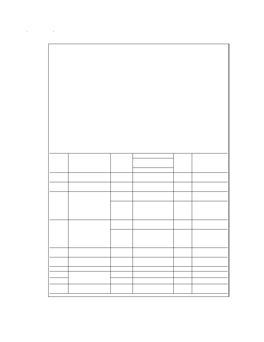
Absolute Maximum Ratings
(Note 1)
If Military/Aerospace specified devices are required,
please contact the National Semiconductor Sales Office/
Distributors for availability and specifications.
Supply Voltage (V
CC
)
-0.5V to +7.0V
DC Input Diode Current (I
IK
)
V
I
= -0.5V
-20 mA
V
I
= V
CC
+ 0.5V
+20 mA
DC Input Voltage (V
I
)
-0.5V to V
CC
+ 0.5V
DC Output Diode Current (I
OK
)
V
O
= -0.5V
-20 mA
V
O
= V
CC
+ 0.5V
+20 mA
DC Output Voltage (V
O
)
-0.5V to V
CC
+ 0.5V
DC Output Source
or Sink Current (I
O
)
±
50 mA
DC V
CC
or Ground Current
per Output Pin (I
CC
or I
GND
)
±
50 mA
Storage Temperature (T
STG
)
-65∞C to +150∞C
DC Latch-up Source or
Sink Current
±
300 mA
Junction Temperature (T
J
)
CDIP
175∞C
Recommended Operating
Conditions
Supply Voltage V
CC
'ACTQ
4.5V to 5.5V
Input Voltage (V
I
)
0V to V
CC
Output Voltage (V
O
)
0V to V
CC
Operating Temperature (T
A
) (Note 2)
54ACTQ
-55∞C to +125∞C
Minimum Input Edge Rate
V/
t
'ACTQ Devices
V
IN
from 0.8V to 2.0V
V
CC
@
4.5V, 5.5V
125 mV/ns
Note 1: Absolute maximum ratings are those values beyond which damage
to the device may occur. The databook specifications should be met, without
exception, to ensure that the system design is reliable over its power supply,
temperature, and output/input loading variables. National does not recom-
mend operation of FACT
Æ
circuits outside databook specifications.
Note 2: All commercial packaging is not recommended for applications re-
quiring greater than 2000 temperature cycles from -40∞C to +125∞C.
DC Characteristics for 'ACTQ Family Devices
54ACTQ
Symbol
Parameter
V
CC
T
A
=
Units
Conditions
(V)
-55∞C to +125∞C
Guaranteed Limits
V
IH
Minimum High Level
4.5
2.0
V
V
OUT
= 0.1V
Input Voltage
5.5
2.0
or V
CC
- 0.1V
V
IL
Maximum Low Level
4.5
0.8
V
V
OUT
= 0.1V
Input Voltage
5.5
0.8
or V
CC
- 0.1V
V
OH
Minimum High Level
4.5
4.4
V
I
OUT
= -50 µA
Output Voltage
5.5
5.4
(Note 3)
V
IN
= V
IL
or V
IH
4.5
3.70
V
I
OH
= -24 mA
5.5
4.70
I
OH
= -24 mA
V
OL
Maximum Low Level
4.5
0.1
V
I
OUT
= 50 µA
Output Voltage
5.5
0.1
(Note 3)
V
IN
= V
IL
or V
IH
4.5
0.50
V
I
OL
= 24 mA
5.5
0.50
I
OL
= 24 mA
I
IN
Maximum Input
5.5
±
1.0
µA
V
I
= V
CC
, GND
Leakage Current
I
OZT
Maximum I/O
5.5
±
10
µA
V
(OE) =
V
IL
, V
IH
Leakage Current
V
O
= V
CC
, GND
I
CCT
Maximum I
CC
/Input
5.5
1.6
mA
V
I
= V
CC
- 2.1V
I
OLD
Minimum Dynamic
Output Current
(Note 4)
5.5
mA
V
OLD
= 1.65V Max
I
OHD
5.5
-50
mA
V
OHD
= 3.85V Min
I
CC
Maximum Quiescent
5.5
160.0
µA
V
IN
= V
CC
Supply Current
or GND (Note 5)
www.national.com
4
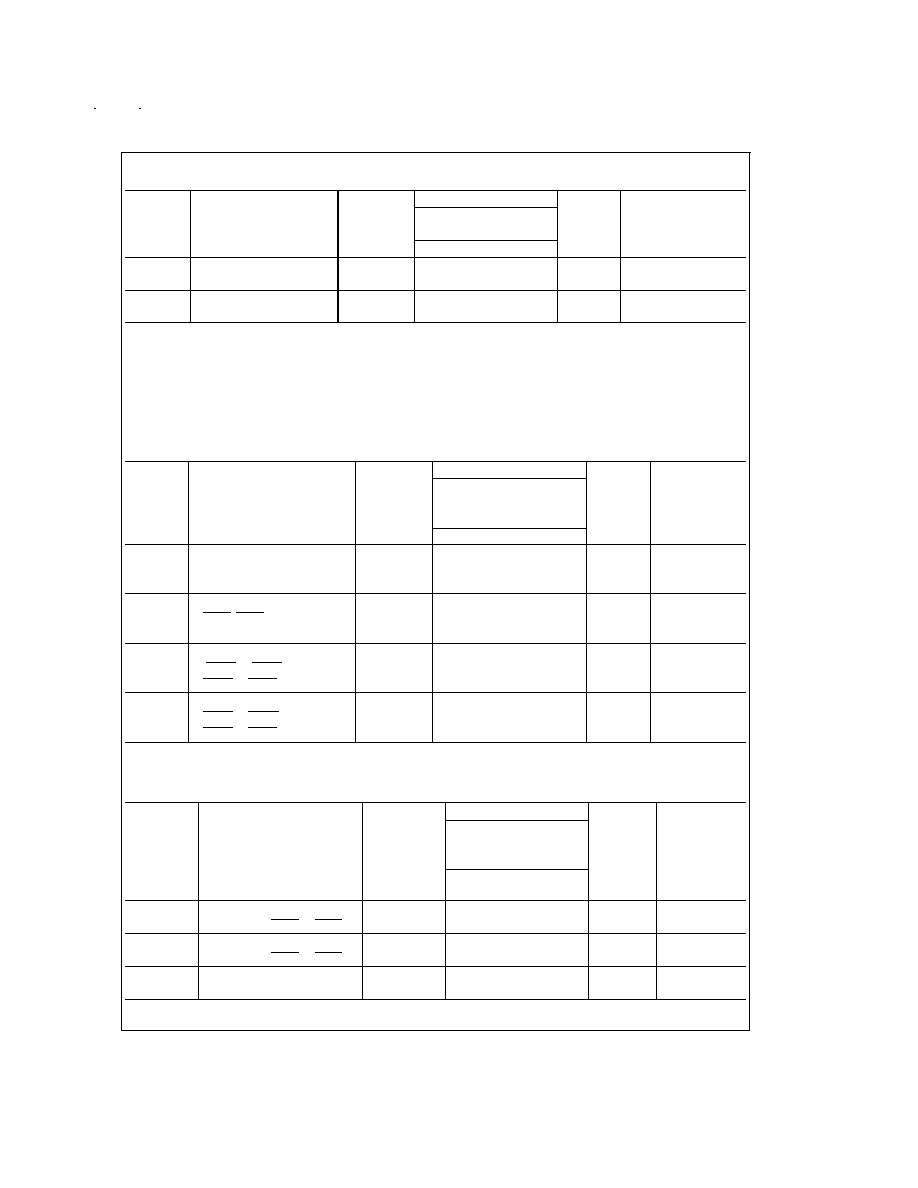
DC Characteristics for 'ACTQ Family Devices
(Continued)
54ACTQ
Symbol
Parameter
V
CC
T
A
=
Units
Conditions
(V)
-55∞C to +125∞C
Guaranteed Limits
V
OLP
Quiet Output
5.0
1.5
V
(Notes 6, 7)
Maximum Dynamic V
OL
V
OLV
Quiet Output
5.0
-1.2
V
(Notes 6, 7)
Minimum Dynamic V
OL
Note 3: Maximum of 8 outputs loaded; thresholds on input associated with output under test.
Note 4: Maximum test duration 2.0 ms, one output loaded at a time.
Note 5: I
CC
for 54ACTQ
@
25∞C is identical to 74ACTQ
@
25∞C.
Note 6: Plastic DIP package.
Note 7: Max number of outputs defined as (n). (n-1) Data Inputs are driven 0V to 3V, one output
@
GND.
Note 8: Max number of Data Inputs (n) switching. (n≠1) Inputs switching 0V to 3V ('ACTQ). Input-under-test switching: 3V to threshold (V
ILD
), 0V to threshold (V
IHD
),
f = 1 MHz.
AC Electrical Characteristics
54ACTQ
Fig.
No.
V
CC
(V)
(Note 9)
T
A
= -55∞C
Symbol
Parameter
to +125∞C
Units
C
L
= 50 pF
Min
Max
t
PLH
Propagation Delay
t
PHL
Transparent Mode
5.0
2.0
9.5
ns
Figure 4
A
n
to B
n
or B
n
to A
n
t
PLH
Propagation Delay
Figure 4
t
PHL
LEBA, LEAB
5.0
2.0
11.0
ns
to A
n
, B
n
t
PZH
Output Enable Time
Figure 6
t
PZL
OEBA or OEAB to A
n
or B
n
5.0
1.5
13.0
ns
CEBA or CEAB to A
n
or B
n
t
PHZ
Output Disable Time
Figure 6
t
PLZ
OEBA or OEAB to A
n
or B
n
5.0
1.5
9.0
ns
CEBA or CEAB to A
n
or B
n
Note 9: Voltage Range 5.0 is 5.0V
±
0.5V
AC Operating Requirements
54ACTQ
Fig.
No.
V
CC
(V)
(Note 10)
T
A
= -55∞C
Symbol
Parameter
to +125∞C
Units
C
L
= 50 pF
Guaranteed
Minimum
t
s
Setup Time, HIGH or LOW
5.0
3.0
ns
Figure 7
A
n
or B
n
to LEBA or LEAB
t
h
Hold Time, HIGH or LOW
5.0
1.5
ns
Figure 7
A
n
or B
n
to LEBA or LEAB
t
w
Latch Enable
5.0
4.0
ns
Figure 5
Pulse Width, LOW
Note 10: Voltage Range 5.0 is 5.0V
±
0.5V
www.national.com
5
Capacitance
Symbol
Parameter
Typ
Units
Conditions
C
IN
Input Capacitance
4.5
pF
V
CC
= OPEN
C
PD
Power Dissipation
70.0
pF
V
CC
= 5.0V
Capacitance
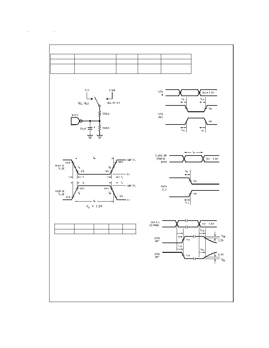
AC Loading
AC Waveforms
DS100233-10
*Includes jig and probe capacitance
FIGURE 1. Standard AC Test Load
DS100233-11
FIGURE 2. Test Input Signal Levels
Amplitude
Rep. Rate
t
w
t
r
t
f
3.0V
1 MHz
500 ns
2.5 ns
2.5 ns
FIGURE 3. Test Input Signal Requirements
DS100233-12
FIGURE 4. Propagation Delay Waveforms for Inverting
and Non-Inverting Functions
DS100233-13
FIGURE 5. Propagation Delay, Pulse Width Waveforms
DS100233-14
FIGURE 6. TRI-STATE Output High and Low Enable
and Disable Time
www.national.com
6

AC Waveforms
(Continued)
DS100233-15
FIGURE 7. Setup Time, Hold Time and Recovery Time Waveforms
www.national.com
7

8

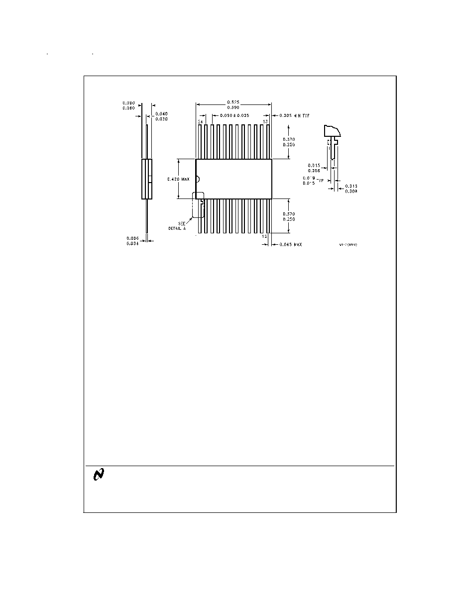
Physical Dimensions
inches (millimeters) unless otherwise noted
28-Terminal Ceramic Leadless Chip Carrier (L)
NS Package Number E28A
24-Lead Ceramic Dual-In-Line Package (D)
NS Package Number J24F
www.national.com
9
Physical Dimensions
inches (millimeters) unless otherwise noted (Continued)
LIFE SUPPORT POLICY
NATIONAL'S PRODUCTS ARE NOT AUTHORIZED FOR USE AS CRITICAL COMPONENTS IN LIFE SUPPORT DE-
VICES OR SYSTEMS WITHOUT THE EXPRESS WRITTEN APPROVAL OF THE PRESIDENT OF NATIONAL SEMI-
CONDUCTOR CORPORATION. As used herein:
1. Life support devices or systems are devices or sys-
tems which, (a) are intended for surgical implant into
the body, or (b) support or sustain life, and whose fail-
ure to perform when properly used in accordance
with instructions for use provided in the labeling, can
be reasonably expected to result in a significant injury
to the user.
2. A critical component in any component of a life support
device or system whose failure to perform can be rea-
sonably expected to cause the failure of the life support
device or system, or to affect its safety or effectiveness.
National Semiconductor
Corporation
Americas
Tel: 1-800-272-9959
Fax: 1-800-737-7018
Email: support@nsc.com
www.national.com
National Semiconductor
Europe
Fax: +49 (0) 1 80-530 85 86
Email: europe.support@nsc.com
Deutsch Tel: +49 (0) 1 80-530 85 85
English
Tel: +49 (0) 1 80-532 78 32
FranÁais Tel: +49 (0) 1 80-532 93 58
Italiano
Tel: +49 (0) 1 80-534 16 80
National Semiconductor
Asia Pacific Customer
Response Group
Tel: 65-2544466
Fax: 65-2504466
Email: sea.support@nsc.com
National Semiconductor
Japan Ltd.
Tel: 81-3-5620-6175
Fax: 81-3-5620-6179
24-Lead Ceramic Flatpak (F)
NS Package Number W24C
54ACTQ543
Quiet
Series
Octal
Registered
T
ransceiver
with
TRI-ST
A
T
E
Outputs
National does not assume any responsibility for use of any circuitry described, no circuit patent licenses are implied and National reserves the right at any time without notice to change said circuitry and specifications.