54ACTQ821
Quiet Series 10-Bit D Flip-Flop with TRI-STATE
Æ
Outputs
General Description
The ACTQ821 is a 10-bit D flip-flop with non-inverting
TRI-STATE outputs arranged in a broadside pinout. The
ACTQ821 utilizes NSC Quiet Series technology to guaran-
tee quiet output switching and improved dynamic threshold
performance. FACT Quiet Series
TM
features GTO
TM
output
control and undershoot corrector in addition to a split ground
bus for superior performance.
Features
n
Guaranteed simultaneous switching noise level and
dynamic threshold performance
n
Non-inverting TRI-STATE outputs for bus interfacing
n
4 kV minimum ESD immunity
n
Outputs source/sink 24 mA
n
Functionally identical to the AM29821
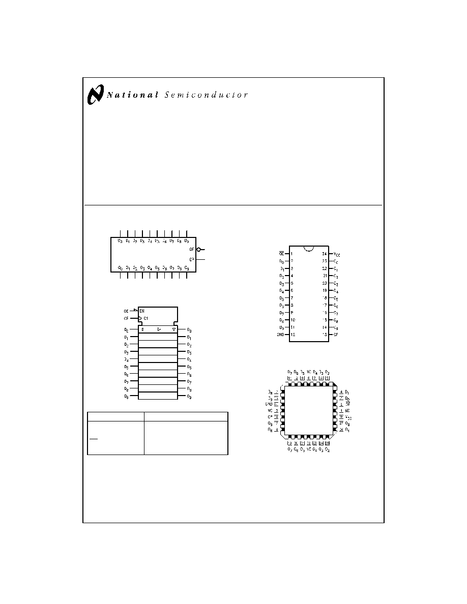
Logic Symbols
Pin Names
Description
D
0
≠D
9
Data Inputs
O
0
≠O
9
Data Outputs
OE
Output Enable Input
CP
Clock Input
Connection Diagrams
GTO
TM
is a trademark of National Semiconductor Corporation.
TRI-STATE
Æ
is a registered trademark of National Semiconductor Corporation.
FACT
Æ
is a registered trademark of Fairchild Semiconductor Corporation.
FACT Quiet Series
TM
is a trademark of Fairchild Semiconductor Corporation.
DS100247-1
IEEE/IEC
DS100247-2
Pin Assignment
for DIP and Flatpak
DS100247-3
Pin Assignment for LCC
DS100247-4
August 1998
54ACTQ821
Quiet
Series
10-Bit
D
Flip-Flop
with
TRI-ST
A
T
E
Outputs
© 1998 National Semiconductor Corporation
DS100247
www.national.com
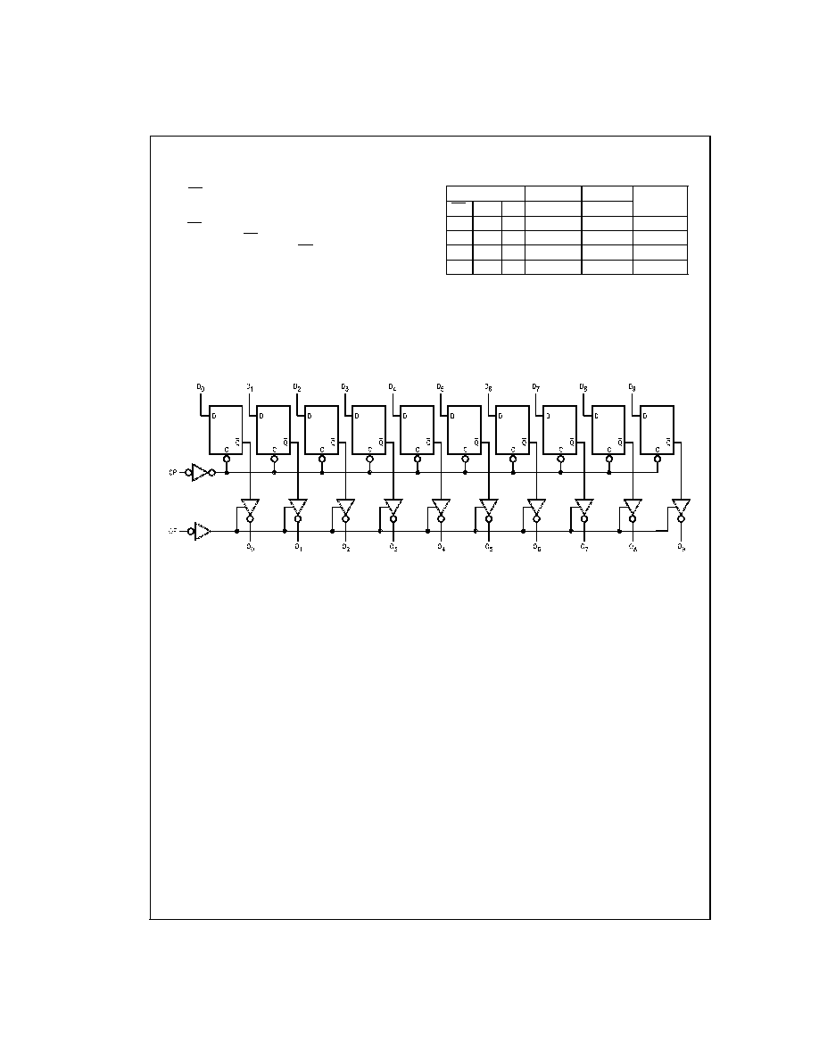
Functional Description
The ACTQ821 consists of ten D-type edge-triggered
flip-flops. The buffered Clock (CP) and buffered Output En-
able (OE) are common to all flip-flops. The flip-flops will store
the state of their individual D inputs that meet the setup and
hold time requirements on the LOW-to-HIGH CP transition.
With OE LOW the contents of the flip-flops are available at
the outputs. When OE is HIGH the outputs go to the high im-
pedance state. Operation of the OE input does not affect the
state of the flip-flops.
The ACTQ821 is functionally and pin compatible with the
AM29821.
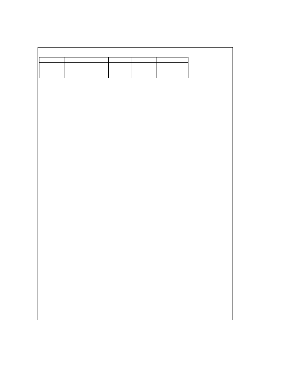
Function Table
Inputs
Internal
Outputs
Function
OE
CP
D
Q
O
H
N
L
L
Z
High Z
H
N
H
H
Z
High Z
L
N
L
L
L
Load
L
N
H
H
H
Load
H = HIGH Voltage Level
L = LOW Voltage Level
Z = HIGH Impedance
N
= LOW-to-HIGH Clock Transition
Logic Diagram
DS100247-5
Please note that this diagram is provided only for the understanding of logic operations and should not be used to estimate propagation delays.
www.national.com
2
Absolute Maximum Ratings
(Note 1)
If Military/Aerospace specified devices are required,
please contact the National Semiconductor Sales Office/
Distributors for availability and specifications.
Supply Voltage (V
CC
)
-0.5V to +7.0V
DC Input Diode Current (I
IK
)
V
I
= -0.5V
-20 mA
V
I
= V
CC
+ 0.5V
+20 mA
DC Input Voltage (V
I
)
-0.5V to V
CC
+ 0.5V
DC Output Diode Current (I
OK
)
V
O
= -0.5V
-20 mA
V
O
= V
CC
+ 0.5V
+20 mA
DC Output Voltage (V
O
)
-0.5V to V
CC
+ 0.5V
DC Output Source
or Sink Current (I
O
)
±
50 mA
DC V
CC
or Ground Current
per Output Pin (I
CC
or I
GND
)
±
50 mA
Storage Temperature (T
STG
)
-65∞C to +150∞C
DC Latch-Up Source
or Sink Current
±
300 mA
Junction Temperature (T
J
)
CDIP
175∞C
Recommended Operating
Conditions
Supply Voltage (V
CC
)
'ACTQ
4.5V to 5.5V
Input Voltage (V
I
)
0V to V
CC
Output Voltage (V
O
)
0V to V
CC
Operating Temperature (T
A
)
54ACTQ
-55∞C to +125∞C
Minimum Input Edge Rate
V/
t
'ACTQ Devices
V
IN
from 0.8V to 2.0V
V
CC
@
4.5V, 5.5V
125 mV/ns
Note 1: Absolute maximum ratings are those values beyond which damage
to the device may occur. The databook specifications should be met, without
exception, to ensure that the system design is reliable over its power supply,
temperature, and output/input loading variables. National does not recom-
mend operation of FACT
Æ
circuits outside databook specifications.
Note 2: All commercial packaging is not recommended for applications re-
quiring greater than 2000 temperature cycles from -40∞C to +125∞C.
DC Electrical Characteristics for 'ACTQ Family Devices
54ACTQ
Symbol
Parameter
V
CC
T
A
=
Units
Conditions
(V)
-55∞C to +125∞C
Guaranteed
Limits
V
IH
Minimum High Level
4.5
2.0
V
V
OUT
= 0.1V
Input Voltage
5.5
2.0
or V
CC
- 0.1V
V
IL
Maximum Low Level
4.5
0.8
V
V
OUT
= 0.1V
Input Voltage
5.5
0.8
or V
CC
- 0.1V
V
OH
Minimum High Level
4.5
4.4
V
I
OUT
= -50 µA
Output Voltage
5.5
5.4
(Note 3)
V
IN
= V
IL
or V
IH
4.5
3.70
V
I
OH
= -24 mA
5.5
4.70
I
OH
= -24 mA
V
OL
Maximum Low Level
4.5
0.1
V
I
OUT
= 50 µA
Output Voltage
5.5
0.1
(Note 3)
V
IN
= V
IL
or V
IH
4.5
0.50
V
I
OL
= 24 mA
5.5
0.50
I
OL
= 24 mA
I
IN
Maximum Input
5.5
±
1.0
µA
V
I
= V
CC
, GND
Leakage Current
I
OZ
Maximum TRI-STATE
5.5
±
10.0
µA
V
I
= V
IL
, V
IH
Leakage Current
V
O
= V
CC
, GND
I
CCT
Maximum I
CC
/Input
5.5
1.6
mA
V
I
= V
CC
- 2.1V
I
OLD
(Note 4)
Minimum Dynamic
Output Current
5.5
50
mA
V
OLD
= 1.65V Max
I
OHD
5.5
-50
mA
V
OHD
= 3.85V Min
3
www.national.com
DC Electrical Characteristics for 'ACTQ Family Devices
(Continued)
54ACTQ
Symbol
Parameter
V
CC
T
A
=
Units
Conditions
(V)
-55∞C to +125∞C
Guaranteed
Limits
I
CC
Maximum Quiescent
5.5
160.0
µA
V
IN
= V
CC
Supply Current
or GND (Note 5)
V
OLP
Quiet Output
5.0
V
(Notes 6, 7)
Maximum Dynamic V
OL
V
OLV
Quiet Output
5.0
V
(Notes 6, 7)
Minimum Dynamic V
OL
Note 3: All outputs loaded; thresholds on input associated with output under test.
Note 4: Maximum test duration 2.0 ms, one output loaded at a time.
Note 5: I
CC
for 54ACTQ
@
25∞C is identical to 74ACTQ
@
25∞C.
Note 6: Plastic DIP package.
Note 7: Max number of outputs defined as (n). Data inputs are driven 0V to 3V. One output
@
GND.
Note 8: Maximum number of data inputs (n) switching. (n-1) inputs switching 0V to 3V ('ACTQ). Input-under-test switching: 3V to threshold (V
ILD
), 0V to threshold
(V
IHD
), f = 1 MHz.
AC Electrical Characteristics
54ACTQ
V
CC
T
A
= -55∞C
Fig.
Symbol
Parameter
(V)
to +125∞C
Units
No.
(Note 9)
C
L
= 50 pF
Min
Max
f
max
Maximum Clock
5.0
95
MHz
Frequency
t
PLH
,
Propagation Delay
5.0
2.5
11.5
ns
t
PHL
CP to O
n
t
PZH
,
Output Enable Time
5.0
2.5
13.0
ns
t
PZL
OE to O
n
t
PHZ
,
Output Disable Time
5.0
1.0
9.0
ns
t
PLZ
OE to O
n
Note 9: Voltage Range 5.0 is 5.0V
±
0.5V
Note 10: Skew is defined as the absolute value of the difference between the actual propagation delay for any two outputs within the same packaged device. The
specification applies to any outputs switching in the same direction, either HIGH to LOW (t
OSHL
) or LOW to HIGH (t
OSLH
). Parameter guaranteed by design. Not
tested.
AC Operating Requirements
54ACTQ
V
CC
T
A
= -55∞C
Fig.
Symbol
Parameter
(V)
to +125∞C
Units
No.
(Note 11)
C
L
= 50 pF
Guaranteed Minimum
t
s
Setup Time, HIGH or LOW
5.0
3.0
ns
D
n
to CP
t
h
Hold Time, HIGH or LOW
5.0
2.0
ns
D
n
to CP
t
w
CP Pulse Width
5.0
4.0
ns
HIGH or LOW
Note 11: Voltage Range 5.0 is 5.0V
±
0.5V
www.national.com
4
Capacitance
Symbol
Parameter
Typ
Units
Conditions
C
IN
Input Capacitance
4.5
pF
V
CC
= OPEN
C
PD
Power Dissipation
55.0
pF
V
CC
= 5.0V
Capacitance
5
www.national.com